EP0657796A2 - Générateur d'horloge et comparateur de phase pour l'utilisation dans un tel générateur d'horloge - Google Patents
Générateur d'horloge et comparateur de phase pour l'utilisation dans un tel générateur d'horloge Download PDFInfo
- Publication number
- EP0657796A2 EP0657796A2 EP94119499A EP94119499A EP0657796A2 EP 0657796 A2 EP0657796 A2 EP 0657796A2 EP 94119499 A EP94119499 A EP 94119499A EP 94119499 A EP94119499 A EP 94119499A EP 0657796 A2 EP0657796 A2 EP 0657796A2
- Authority
- EP
- European Patent Office
- Prior art keywords
- output
- delay
- phase comparator
- clock generator
- input
- Prior art date
- Legal status (The legal status is an assumption and is not a legal conclusion. Google has not performed a legal analysis and makes no representation as to the accuracy of the status listed.)
- Granted
Links
- 230000009977 dual effect Effects 0.000 claims description 11
- 230000001965 increasing effect Effects 0.000 claims description 7
- 230000004913 activation Effects 0.000 claims description 6
- 230000003213 activating effect Effects 0.000 claims description 4
- 230000005669 field effect Effects 0.000 claims description 4
- 230000008859 change Effects 0.000 description 13
- 238000010586 diagram Methods 0.000 description 6
- 238000004519 manufacturing process Methods 0.000 description 3
- 239000013078 crystal Substances 0.000 description 2
- 239000010453 quartz Substances 0.000 description 2
- 230000004044 response Effects 0.000 description 2
- VYPSYNLAJGMNEJ-UHFFFAOYSA-N silicon dioxide Inorganic materials O=[Si]=O VYPSYNLAJGMNEJ-UHFFFAOYSA-N 0.000 description 2
- 230000009471 action Effects 0.000 description 1
- 230000008901 benefit Effects 0.000 description 1
- 230000000295 complement effect Effects 0.000 description 1
- 230000001934 delay Effects 0.000 description 1
- 230000000694 effects Effects 0.000 description 1
- 230000003028 elevating effect Effects 0.000 description 1
- 230000010355 oscillation Effects 0.000 description 1
- 230000010363 phase shift Effects 0.000 description 1
- 230000000630 rising effect Effects 0.000 description 1
- 238000004904 shortening Methods 0.000 description 1
Images


Classifications
-
- H—ELECTRICITY
- H03—ELECTRONIC CIRCUITRY
- H03K—PULSE TECHNIQUE
- H03K3/00—Circuits for generating electric pulses; Monostable, bistable or multistable circuits
-
- G—PHYSICS
- G06—COMPUTING; CALCULATING OR COUNTING
- G06F—ELECTRIC DIGITAL DATA PROCESSING
- G06F1/00—Details not covered by groups G06F3/00 - G06F13/00 and G06F21/00
- G06F1/04—Generating or distributing clock signals or signals derived directly therefrom
- G06F1/08—Clock generators with changeable or programmable clock frequency
-
- H—ELECTRICITY
- H03—ELECTRONIC CIRCUITRY
- H03K—PULSE TECHNIQUE
- H03K5/00—Manipulating of pulses not covered by one of the other main groups of this subclass
- H03K5/13—Arrangements having a single output and transforming input signals into pulses delivered at desired time intervals
- H03K5/135—Arrangements having a single output and transforming input signals into pulses delivered at desired time intervals by the use of time reference signals, e.g. clock signals
-
- H—ELECTRICITY
- H03—ELECTRONIC CIRCUITRY
- H03L—AUTOMATIC CONTROL, STARTING, SYNCHRONISATION OR STABILISATION OF GENERATORS OF ELECTRONIC OSCILLATIONS OR PULSES
- H03L7/00—Automatic control of frequency or phase; Synchronisation
- H03L7/06—Automatic control of frequency or phase; Synchronisation using a reference signal applied to a frequency- or phase-locked loop
- H03L7/08—Details of the phase-locked loop
- H03L7/085—Details of the phase-locked loop concerning mainly the frequency- or phase-detection arrangement including the filtering or amplification of its output signal
- H03L7/089—Details of the phase-locked loop concerning mainly the frequency- or phase-detection arrangement including the filtering or amplification of its output signal the phase or frequency detector generating up-down pulses
-
- H—ELECTRICITY
- H03—ELECTRONIC CIRCUITRY
- H03L—AUTOMATIC CONTROL, STARTING, SYNCHRONISATION OR STABILISATION OF GENERATORS OF ELECTRONIC OSCILLATIONS OR PULSES
- H03L7/00—Automatic control of frequency or phase; Synchronisation
- H03L7/06—Automatic control of frequency or phase; Synchronisation using a reference signal applied to a frequency- or phase-locked loop
- H03L7/08—Details of the phase-locked loop
- H03L7/099—Details of the phase-locked loop concerning mainly the controlled oscillator of the loop
- H03L7/0995—Details of the phase-locked loop concerning mainly the controlled oscillator of the loop the oscillator comprising a ring oscillator
- H03L7/0997—Controlling the number of delay elements connected in series in the ring oscillator
Definitions
- the invention relates to a clock generator of the kind as stated in the preamble of Claim 1; it also relating to a digital phase comparator according to the preamble of Claim 15 for use in such a clock generator.
- a voltage-controlled oscillator is provided as a rule as the adjustable oscillator, a low-pass filter being additionally connected between the voltage-controlled oscillator and the phase comparator.
- the output of the voltage-controlled oscillator is fed back to an input of the phase comparator to achieve a phase-locked loop (PLL).
- PLL phase-locked loop
- the object of the invention is to create a clock generator together with a suitable phase comparator of the aforementioned kind which despite its simpler configuration and relatively low current consumption ensures reliable operation, permitting a more or less precise adjustment of the frequency in each case.
- the adjustable oscillator being a digital delay chain
- the frequency divider being a digital programmable frequency divider and by connecting between the output of the phase comparator and the delay chain a digital up-down counter, the counting direction of which is determined by the output signal of the phase comparator and by means of which the corresponding length of the delay chain is adjustable.
- the delay chain is preferably assigned an interpolation logic comprising a dual counter which is clocked by the output signal of the delay chain.
- the count of this dual counter is combined with the value of a number of least-significant bits of the output signal of the up-down counter to define, as a function of the value of these least-significant bits, the number of changes in the length of the delay chain by one step at a time for each clock cycle whilst the remaining most-significant bits directly address the delay chain.
- the corresponding length of the delay chain and thus the frequency in each case can be adjusted by activating a corresponding loop inverter which defines the inversion point in each case at which the forward branch of the delay chain is directly connected with the return branch thereof.
- Resetting the delay elements as defined by function, for instance on power up, is ensured in particular by the delay chain having preferably alternating delay elements of a first kind, the outputs of which are logical 0 in the reset condition, and delay elements of a second kind the outputs of which are logical 1 in the reset condition. Accordingly all connecting points of the delay chain can be reset, if required, to a precisely defined initial status, the output of the selected loop inverter assuming the correct value so that unwanted signal spikes are avoided when changes are later made to the length of the chain.
- the maximum frequency step from one delay element to the next should possibly not exceed 1/6. Accordingly it is good practice to compose the delay chain of at least 6 delay elements.
- the delay elements inserted with increasing chain length may have a higher delay than necessary for a shorter chain length and thus, in particular, the change in frequency as a percentage in the transfer from one delay element to the next may be maintained constant.
- the inverters of the delay elements preferably contain current mirrors by means of which the driver currents in each case can be limited with no problem.
- the inverters each contain a p-type MOS field-effect transistor and an n-type MOS field-effect transistor, connected in series with a switching transistor.
- the delay of the individual delay elements can be usefully defined by the channel length of the current mirror transistors defining the driver current.
- phase comparators of the kind as stated in the preamble of claim 15 are already known, these are, however, employed as a rule in conjunction with voltage-controlled oscillators.
- Using these conventional phase comparators in a digital clock generator is hampered by a series of drawbacks, for instance, their up and down outputs also being regularly activated at the same time, resulting particularly in the activation of a digital up-down counter at least being rendered difficult.
- the digital phase comparator according to the invention which can be employed in particular in a digital clock generator contains means to lock the non-activated output in its non-activated status as long as the other output is being reset.
- activating a digital up-down counter in particular is substantially simplified, it being for instance sufficient for this purpose to output the digital phase comparator by a simple RS flip-flop, the set and reset inputs of which are to be connected to the two outputs of the digital phase comparator.
- This output RS flip-flop then furnishes at one output a single activating signal which preferably serves to activate the digital up-down counter of the clock generator according to the invention, via which the delay chain serving as an adjustable oscillator is controlled.
- the embodiment of the digital clock generator according to the invention as shown in Fig. 1 contains a reference oscillator 10, an adjustable ring oscillator in the form of a digital closed digital chain 12, a digital programmable frequency divider 14 and a digital phase comparator 16.
- the digital programmable frequency divider 14 is connected between the output of the delay chain 12 and one input of the phase comparator 16.
- the output of the reference oscillator 10 is connected to a further input of the phase comparator 16.
- the up-down counter 18 is connected to the output of the phase comparator 16.
- the output of this up-down counter 18 is connected at the one end to the delay chain 12 and, at the other, to an interpolation logic circuit 20, by means of which the delay chain 12 can be activated just the same as via the output of the up-down counter 18 as indicated by the arrows entered in the Fig.
- the interpolation logic 20 assigned to the delay chain 12 contains a dual counter 22 which is clocked by the output signal of the delay chain 12.
- the count of the dual counter 22 is combined with the value of a number of least-significant bits of the output signal of the up-down counter 18 so that the number of changes in the length of the chain is defined by one step each for one corresponding clock cycle as a function of the value of the least-significant bits.
- the remaining most significant bits of the up-down counter 18 serve to address the delay chain directly by means as described in more detail below.
- the output clock signal T A furnishing the set frequency is fed back via the digital frequency divider 14 to the input V2 of the phase comparator 16. Apart from the interpolation logic 20 thus output clock signal T A is also preferably used to clock the up-down counter 18.
- the reference oscillator 10 contains a 32 kHz oscillator quartz crystal.
- the output clock signal T A is divided by the number 32 by the frequency divider 14.
- the delay chain 12 is composed of 32 weighted delay elements 24, 26 connected in series (viz. also Figs. 2 thru 5).
- the up-down counter 18 is a 10-bit counter whilst the dual counter 22 used for the interpolation logic 20 is a 5-bit counter.
- the five least-significant bits of the output signal of the up-down counter 18 are combined accordingly with the count of the dual counter 22, whereas the five most-significant bits of the output signal of the up-down counter 18 are used to directly address the delay chain 12.
- the output signal V1 of the reference oscillator 10 is compared to the output signal V2 of the programmable frequency divider 14 preset to the divisor 32.
- the phase comparator 16 furnishes an output signal, by means of which the counting direction of the up-down counter 18 is determined.
- the delay chain 12 is adjusted as regards its length so that the frequency deviation established by the phase comparator 16 is zero.
- Figs. 2 and 3 are simple schematic representations of the digital closed delay chain 12 containing delay elements 24 alternately of the first kind, the outputs of which when reset (viz. Fig. 2) have the logic value 0, and delay elements 26 of a second kind, the outputs of which when reset have the logic value 1 In these Figs 2 and 3 each resulting output value of the delay elements 24, 26 in the reset condition is indicated by inverted commas.
- Fig. 2 shows the status of the delay elements 24, 26 directly after resetting, whereby the status of the output at the end of the reset path 44 has just changed to the value 0 whilst this value also being applied at the same time to the input of the forward path 46 is still to cause a change in the status at the output of the first inverter of this forward path 46.
- the inverters involved thus have the output values 0, 1, 0, 1, ...one after the other in the forward direction.
- an inverter 22 in the form of a ladder rung is connected between the forward path 46 and the return path 44.
- this transverse inverter 32 the length of the delay chain 12 can be shortened or lengthened by ways and means as described in more detail below. In this arrangement only one inverter 32 at a time is activated, upon which the remainder of the delay chain 12 (shown on the right in Figs. 2 and 3 ) in each case is no longer active.
- Fig. 3 shows the status of the delay chain 12 immediately after the output of the delay chain 12 has changed its values from 0 to 1 and after the complete chain as shown in Fig.3 has been activated. Accordingly the outputs of the inverters in the forward path 46 and the return path 44 alternatively have the values 1, 0, 1, 0 and so on. In the illustration shown in Fig. 3 the value 1 at the output is still to affect the input of the first inverter of the forward path 46 and thus its output is still 1. By selecting an inverter 32 oriented transversely the chain can be suitably shortened, causing the frequency to be increased accordingly.
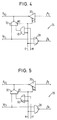
- Fig. 4 the circuit diagram of a delay element 24 of the first kind is shown which in the reset condition has the value 0 at the two outputs V A and R A .
- FIG. 5 shows a delay element 26 of the second kind, the two outputs V A and R A of which have the value 0 in the reset condition.
- Each of the delay elements 24, 26 alternately of the first and second kind in the delay chain 12 is assigned a forward inverter 28 and a return inverter 30 as well as a loop inverter 32 which when activated allows the corresponding length of the chain to be adjusted.
- the delay elements 24, 26 further contain two control inputs E, N via each of which their forward inverter 28 and return inverter 30 or their loop inverter 32 can be activated or the corresponding delay element 24, 26 reset.
- addressing the delay chain 12 via the control inputs E, N is such that only one single loop inverter 32 at a time is activated.
- resetting the delay elements 24, 26 is best done automatically on every power up.
- the forward inverter contains a NOR gate 28 with the forward output V A .
- the return inverter 30 with the return output R A has an inverted control input IS via which it can be activated when a control signal 0 is applied.
- the loop inverter contains a NOR gate 32, the output of which is connected to the output R A of the return inverter 30.
- This NOR gate 32 has a non-inverted control input NS via which it can be activated by an applied control signal 0.
- the forward input V E of the delay element 24 is connected to an input of the NOR gate 32 and to an input of the NOR gate 28.
- One other input of the NOR gate 32 is connected to the output of an AND gate 48, the two inputs of which are connected to the control input E and the control input N respectively of the the delay element 24.
- the control input E is connected to yet a further input of the NOR gate 28.
- the other control input E is connected to both the inverting control input IS of the return inverter 30 and to the non-inverting control input NS of the NOR gate 32.
- this delay element 24 of the first kind is evident from the following truth table: indicating that the two outputs V A and R A of the delay element 24 are reset to the value 0 when both control inputs E, N have the value 1.
- the loop inverter 32 is then activated or addressed when the control input W has the value 1 and the control input N the value 0.
- the value of the forward output V A equals 0 whilst the reference oscillator R A equals the inverted value ⁇ V E of the forward input V E .
- the length of the delay chain 12 is determined by this loop inverter 32. The remaining loop inverter remains deactivated.
- the forward input 28 contans a NAND gate 28 and the loop inverter a NAND gate 32.
- An inverting control input IS of the NAND gate 28 is connected together with a non-inverting control input NS of the return input 30 to the control input N of the delay element 26.
- This control input N is further connected to an input of the NAND gate 28 and to an input of an OR gate 50 which has a further input connected to the control input E of the delay element 26.
- the output of the OR gate 50 is connected to an input of the NAND gate 32 which has a further input to which the forward input V E of the delay element 26 is connected. At this forward input V E of the delay element 26 a further input of the NAND gate 28 is connected.
- the forward output V A is formed by the output of this NAND gate 28.
- the output of the return input 30 and the output of the NAND gate 32 are connected to the reference oscillator R A of the delay element 26 whilst the return input R E of the delay element 26 is formed by the input of the return input 30.
- this delay element 26 of the second kind is evident from the following truth table: indicating that each of the two outputs V A and R A of the delay element 26 are reset to the value 1 when both control inputs E, N have the value 1.
- the loop inverter 32 is activated, resulting in the inverted value ⁇ V E of the forward input V E occurring at the return input R A whilst the forward output V A is held at the value 1.
- the delay chain 12 has a delay element 24 of the first kind at the end furnishing the output clock signal T A .
- All inverters 28, 30, 32 contain current mirror circuits to limit the driver current in each case.
- a bias voltage generator furnishes the voltage for gating a p-type MOS FET and an n-type MOS FET connected in series with the switching transistors. Accordingly, the output current of each delay element 24, 26 can easily be determined by the channel length ratios. The width of all transistors and the length of the switching transistors can be reduced to a minimum. To reduce the switching noise between the stages and to avoid charge takeover effects the current mirror transistors can be directly connected to the output.
- the current consumption within the delay chain 12 is mainly determined by the capacitances between the delay elements 24, 26 needing to be repoled.
- the setpoint frequency of 1 MHz should be attained under normal conditions (3 V, 27°C typical fabrication parameters) by roughly half of the delay chain 12 being activated, this leaving enough space to both ends for deviations from the nominal values.
- a capacitance of 2 x 70 fF is achieved for each delay element, for instance, as long as the circuit has been designed for a minimum capacitance.
- the current needed to repole 32 capacitances of 16 delay elements 24, 26 is given by the following:
- the maximum step in frequency from one delay element 24, 26 to the next should not exceed 1/6. Accordingly the delay chain 12 should preferably contain at least six delay elements 24, 26.
- the delay of the various delay elements 24, 26 can be increased with increasing length of the chain without the step in frequency being greater than 1/6.
- the 13th delay element can have twice the delay than that of the first delay element.
- the delay of the various delay elements can simply be increased by correspondingly increasing the channel length of the transistors defining the current in the current mirror concerned. In this way the percentual change in the frequency from one delay element to the next can be maintained more or less constant, whereby the usual deviations in the fabrication parameters are tolerable.
- the first 9 delay elements 24, 26 can furnish a driver current of approx. 10 ⁇ A, the maximum output then being continually reduced.
- the repoling current can be simply changed, for example, by changing the resistor determining the current in the bias voltage generator.
- a conventional CMOS inverter may be employed at least as a loop inverter.
- the frequency divider 14, the interpolation logic circuit 20 and the up-down counter are clocked with the output of the delay chain 12.
- This clock pulse having a frequency of 1 MHz for instance, is divided, by the frequency divider 14 by, for example,32 and compared to the 32 kHz reference frequency in the phase comparator 16.
- the frequency divider 14 is programmable, for example, between 1 and 127.
- the output signal of the phase comparator 16 then dictates the counting direction of the 10 bit up-down counter 18, the five most-significant bits of which directly address the delay chain 12.
- the maximum adjustable frequency is normally limited by the delays of the frequency divider 14, the phase comparator 16, the interpolation logic circuit 20 and the 10 bit up-down counter 18. This loop (turning) point is attained after 1/4 of the clock cycle.
- the five most-significant bits of the up-down counter 18 are used to address the delay chain 12, whilst the remaining five least-significant bits are combined with the outputs of the 5-bit dual counter 22 of the interpolation logic circuit 20.
- the following Table indicates when the delay chain 12 is shortened by one step each time, whereby the output value of the 5-bit dual counter 22 is given in the horizontal direction and the value of the five least-significant bits of the 10 bit up-down counter is given in the vertical direction.
- step change frequency with the value of the five least-significant bits of the up-down counter 18 increases.
- This interpolation logic 20 supports elevating the control frequency in the locked status so that the frequency deviation as a whole is reduced within brief periods of time.
- the phase generator 16 of the clock generator shown in Fig. 1 serves to define the counting direction of the up-down counter 18 in the all-digital loop.
- This up-down counter furnishes a corresponding output signal, by means of which the length of the closed delay chain 12 and thus the setpoint frequency is controlled.
- the digital phase comparator used for this purpose may have, for example, an up output and a down output to establish the counting direction of the up-down counter 18 according to the status of the two input signals V1, V2 (viz. Fig. 1).
- the digital phase comparator can be suitably designed so that, depending on which of the two input signals first assumes its active value, the assigned up output and down output respectively is set to an active value and reset following the other input signal becoming active.
- Phase comparators of this kind are already employed in PLL circuits in which the duty cycle of both outputs is employed as a measure of the deviation in phase and frequency.
- phase comparator cannot, however, be employed directly in the digital clock generator shown in Fig. 1, especially since to activate the up-down counter 18 a discrete control signal is to be preferably provided, by means of which the corresponding counting direction is determined.
- One simple solution of creating such a discrete control signal could be to connect the up and down outputs of the digital phase comparator to the set and reset inputs of a discrete RS flip-flop and to pick off the control signal at one output of this flip-flop.
- this solution may result in noisy voltage spikes when using known digital phase comparators as is evident from Figs. 6 and 7.
- a known digital phase comparator having two inputs for the input signals V1 and V2 and an up output 34 and a down output 36.
- the inputs V1 and V2 of this known digital phase comparator simultaneously form the inputs of two input gates, i.e. NAND gate 52 and NAND gate 54 respectively.
- the output of the NAND gate 52 is connected to the set input S of an RS flip-flop 56 comprising two NAND gates 56', 56'' and, on the other, to an input of an output gate, namely the NAND gate 60.
- the output of the NAND gate 60 is fed back to a further input of the NAND gate 52.
- the output of the NAND gate 60 forms simultaneously the up output 34 of the digital phase comparator.
- the output of the NAND gate 54 is connected on the one hand to the set input S of an RS flip-flop 58 comprising two NAND gates 58', 58'' and, on the other, to an input of an output gate, namely the NAND gate 62.
- the output of the NAND gate 62 is fed back to a further input of the NAND gate 54, the output of the NAND gate 62 forms simultaneously the down output 36 of the digital phase comparator.
- the output Q of the RS flip-flop 56 is connected on the one hand to a further input of the NAND gate 60 and, on the other, to an input of a further NAND gate 64.
- the output Q of the other RS flip-flop 58 is connected on the one hand to a further input of the NAND gate 62 and, on the other, to a further input of NAND gate 64.
- This NAND gate 64 has two further inputs which are connected to the output of the NAND gate 52 and the output of the NAND gate 54 respectively.
- the output of the NAND gate 64 is connected to a third input of the NAND gate 60 as well as to a third input of the NAND gate 62 and, in addition to this, is also connected to the reset input R of the RS flip-flop 56 as well as to the corresponding reset input R of the RS flip-flop 58.
- the NAND gate 64 accordingly serves to reset the up and down outputs 34, 36 of the phase comparator to 1 and the two RS flip-flops 56, 58 to 0.
- the other RS flip-flop 58 will additionally be set to 1.
- the up and down outputs 34, 36 of the digital phase comparator continue to have the value 1.
- the corresponding output 34 and 36 respectively of the phase comparator is set to the active value 0.
- the down output 36 will first be set to the value 0. If then the input signal V1 also reassumes the value 0, the down output 36 previously set to 0 will be reset to 1. In this case, however, a noisy 0 pulse results at the up output 34 (viz. Fig. 7).
- This digital phase comparator comprises in turn two input gates, namely NAND gate 52 and NAND gate 54.
- the input signal V1 is applied to one input of the NAND gate 52 whilst the other input signal V2 is available at one input of the NAND gate 54.
- the output of the NAND gate 52 is connected on the one hand to the set input ⁇ S of an RS flip-flop 56 comprising two NAND gates 56', 56'' and, on the other, to one input of an output gate, namely NAND gate 60.
- the output Q of the RS flip-flop 56 is connected to a further input of the NAND gate 60.
- the output of the NAND gate 60 connected to the up output 34 of the digital phase comparator is fed back to a further input of the NAND gate 52.
- the output of the NAND gate 54 is connected on the one hand to the set input ⁇ S of an RS flip-flop 58 and, on the other, to one input of an output gate, namely NAND gate 62.
- the output Q of the RS flip-flop 58 is connected to a further input of the NAND gate 62.
- the output of the NAND gate 62 forming the down output 36 of the digital phase comparator is fed back to a further input of the NAND gate 54.
- phase comparator As shown in Fig. 8, however, the function of the NAND gate 64 provided in the known phase comparator (viz. Fig. 6) is shared by three NAND gates 40, 42, 68 and a NOR gate 66. In addition a further reset input RÜCK is provided to return the circuit to a defined status preferably on power up.
- a further reset input RÜCK is provided to return the circuit to a defined status preferably on power up.
- output Q of the RS flip-flop 56 is additionally connected to an input of a NAND gate 40, the output of which is connected to a further input of the NAND gate 62.
- output Q of the RS flip-flop 58 is additionally connected to an output of a NAND gate 42. the output of which is connected to a further input of the NAND gate 60.
- One further input of the NAND gate 40 is connected to the output of the NAND gate 52 whilst a further input of the NAND gate 42 is connected to the output of the NAND gate 54.
- the output ⁇ Q of the RS flip-flop 56 is connected to an input of a NOR gate 66 having a further input to which the corresponding output ⁇ Q of the RS flip-flop 58 is connected.
- the output of the NOR gate 66 is connected to one input of a further NAND gate 68 having two further inputs which are connected to the output of the NAND gate 52 and the output of the NAND gate 54 respectively.
- the output of the NAND gate 68 is simultanously connected to both one reset input ⁇ R of the RS flip-flop 56 and one reset input ⁇ R of the RS flip-flop 58.
- the digital phase comparator is provided with an additional reset input RÜCK which is connected to a further reset input R of the RS flip-flop 56, a further reset input ⁇ R of the RS flip-flop 58, a further input of the NAND gate 52 as well as to a further input of the NAND gate 54.
- phase comparator When both input signals V1, V2 are each 0 and both RS flip-flops 56, 58 are reset to 0 (output Q) the up and down outputs 34, 36 of the digital phase comparator according to the invention are reset to 1. In this defined output status the phase comparator can be set in particular by a 0 pulse at the additional reset input RÜCK.
- the assigned RS flip-flop 56 is set to the value 1 (output Q).
- the further RS flip-flop 58 will also be set to the value 1 (output Q) whereby the output of the NOR gate 66 changes in value from 0 to 1 since both the output ⁇ Q of the RS flip-flop 56 as well as the output ⁇ Q of the RS flip-flop 58 each assume the value 0.
- RS flip-flop 58 is first reset to the value 0 (output Q). With value 1 at the output of the NAND gate 54 the value 0 will also occur at first at the output of the NAND gate 68, this also causing the other RS flip-flop 56 to be reset to the value 0 (output Q). Accordingly the up output 34 of the digital phase comparator is reset to the value 1.
- the NAND gate 40 Since the NAND gate 40 first maintains the value 0 at its output, until also the RS flip-flop 56 has been reset to 0 (output Q) and, before then, the output Q of the RS flip-flop 58 has already been set to the value 0, the down output 36 of the digital phase comparator is maintained (locked) to its existing value 1 at the same time as the up output 34 is reset to the value 1.
- the output of the NAND gate 40 again assumes the value 1 after RS flip-flop 56 has been reset, then as soon as the output Q of the RS flip-flop 58 assumes the value 0 it is already assured that the NAND gate 62 continues to retain the value 1 at the down output 36.
- the value 0 materializes at the output of the NOR gate 66, this in turn causing the output of the NAND gate 68 to be reset to the value 1 so that the reset pulse at the output of this NAND gate 68 or at the reset inputs ⁇ R of the two RS flip-flops 56,58 is terminated.
- the down output 36 of the digital phase comparator is first set to 0. Should then the input signal V1 change to the value 0,then the down output 36 too will be reset to 0 without any negative pulse materializing at the up output 34. In this case the NAND gate 42 ensures that the value 1 is maintained or locked at the up output 34.
- a simple RS flip-flop 38 can be used in particular for generating a single activation signal for the up-down counter 18 (viz. Fig. 1) as is evident from Fig. 8.
- this arrangement it is useful to connect the up output 34 to the set input S and the down output 36 to the reset input R of the RS flip-flop 38.
- An output Q of this RS flip-flop 38 then dictates the counting direction of the up-down counter 18 of the digital clock generator shown in Fig. 1.
- the digital phase comparator according to the invention may be put to use, however,not only in all-digital loops such as in particular in the clock generator as shown in Fig. 1 but also, for example, in combination with an oscillator, e.g. in an analog loop.
- any other suitable terminating circuit for generating the single activation signal for the digital up-down counter may be provided.
- phase comparator then preferably setting its up output to the active value until the frequency produced at the output of the frequency divider is more or less the same as the reference frequency.
- Any shift in phase at the set frequency may be counteracted, for example, by reducing the extent of the switching stages in the delay chain and/or by by synchronizing the output signal of the frequency divider with the reference frequency as soon as the phase shift exceeds a critical value, thus enabling the amplitude of any oscillation about the set value (jitter) to be significantly reduced. Since fleeting deviations in frequency are also reduced to a minimum, exceptionally precise adjustment of frequency is possible so that even protocols of an asynchronous data exchange can be made use of.
- Normally closed loop control commences on power up of the full chain length, i.e.at the lowest possible frequency.
- the time need to set the delay chain can be further reduced, for example, by counting the clock pulses generated within one cycle of the reference frequency for the complete chain and calculating the setpoint length, thus enabling the chain to be preset to this calculated length so that the total time needed for adjustment after power up is reduced.
Landscapes
- Physics & Mathematics (AREA)
- Engineering & Computer Science (AREA)
- Theoretical Computer Science (AREA)
- General Engineering & Computer Science (AREA)
- General Physics & Mathematics (AREA)
- Nonlinear Science (AREA)
- Stabilization Of Oscillater, Synchronisation, Frequency Synthesizers (AREA)
- Pulse Circuits (AREA)
Applications Claiming Priority (2)
| Application Number | Priority Date | Filing Date | Title |
|---|---|---|---|
| DE4342266A DE4342266C2 (de) | 1993-12-10 | 1993-12-10 | Taktgenerator sowie Phasenkomparator zur Verwendung in einem solchen Taktgenerator |
| DE4342266 | 1993-12-10 |
Publications (3)
| Publication Number | Publication Date |
|---|---|
| EP0657796A2 true EP0657796A2 (fr) | 1995-06-14 |
| EP0657796A3 EP0657796A3 (fr) | 1998-09-02 |
| EP0657796B1 EP0657796B1 (fr) | 2005-03-02 |
Family
ID=6504735
Family Applications (1)
| Application Number | Title | Priority Date | Filing Date |
|---|---|---|---|
| EP94119499A Expired - Lifetime EP0657796B1 (fr) | 1993-12-10 | 1994-12-09 | Générateur d'horloge et comparateur de phase pour l'utilisation dans un tel générateur d'horloge |
Country Status (5)
| Country | Link |
|---|---|
| US (1) | US5877641A (fr) |
| EP (1) | EP0657796B1 (fr) |
| JP (1) | JP3841456B2 (fr) |
| KR (1) | KR100345272B1 (fr) |
| DE (2) | DE4342266C2 (fr) |
Cited By (7)
| Publication number | Priority date | Publication date | Assignee | Title |
|---|---|---|---|---|
| EP0866555A2 (fr) * | 1997-03-17 | 1998-09-23 | Sony Corporation | Circuit de retard et oscillateur l'utilisant |
| FR2816074A1 (fr) * | 2000-10-30 | 2002-05-03 | St Microelectronics Sa | Generateur digital precis produisant des signaux d'horloge |
| EP1491985A2 (fr) * | 2003-06-27 | 2004-12-29 | Siemens Aktiengesellschaft | Méthode et dispositif de génération de temps dans une unité de traitement de données |
| WO2007040859A1 (fr) * | 2005-09-30 | 2007-04-12 | Advanced Micro Devices, Inc. | Ligne a retard commandee par tension a multiplexeur enfoui et fonctions d'interpolation |
| CN1319271C (zh) * | 2003-06-11 | 2007-05-30 | 恩益禧电子股份有限公司 | 频谱扩展时钟发生装置 |
| US7256636B2 (en) | 2005-09-16 | 2007-08-14 | Advanced Micro Devices, Inc. | Voltage controlled delay line (VCDL) having embedded multiplexer and interpolation functions |
| CN101030770B (zh) * | 2006-03-03 | 2010-11-03 | 恩益禧电子股份有限公司 | 频谱扩展时钟控制装置及频谱扩展时钟发生装置 |
Families Citing this family (24)
| Publication number | Priority date | Publication date | Assignee | Title |
|---|---|---|---|---|
| US6247138B1 (en) * | 1997-06-12 | 2001-06-12 | Fujitsu Limited | Timing signal generating circuit, semiconductor integrated circuit device and semiconductor integrated circuit system to which the timing signal generating circuit is applied, and signal transmission system |
| EP1012981A1 (fr) * | 1997-09-10 | 2000-06-28 | Siemens Aktiengesellschaft | Circuit permettant de generer un signal de frequence reglable |
| JP3338367B2 (ja) * | 1998-03-25 | 2002-10-28 | 沖電気工業株式会社 | 位相比較器 |
| US6182372B1 (en) * | 1998-08-25 | 2001-02-06 | Trimble Navigation Limited | Interpolation using digital means for range findings in a total station |
| WO2001006696A1 (fr) * | 1999-07-16 | 2001-01-25 | Conexant Systems, Inc. | Appareil et procede pour detecteur de phase autocentre commande par un servomecanisme |
| DE19946764C2 (de) | 1999-09-29 | 2003-09-04 | Siemens Ag | Digitaler Phasenregelkreis |
| JP2001339294A (ja) * | 2000-05-30 | 2001-12-07 | Mitsubishi Electric Corp | Dll回路 |
| EP1211811A1 (fr) * | 2000-11-28 | 2002-06-05 | Koninklijke Philips Electronics N.V. | Dispositif de comparaison de fréquences à faible inertie temporelle |
| EP1244207A1 (fr) * | 2001-03-23 | 2002-09-25 | STMicroelectronics Limited | Comparateur de phase |
| KR100374648B1 (ko) * | 2001-06-28 | 2003-03-03 | 삼성전자주식회사 | 전자파를 감소시키기 위한 위상동기루프회로 및 그의제어방법 |
| JP3719413B2 (ja) * | 2001-12-05 | 2005-11-24 | 日本電気株式会社 | データ伝送システム及びそれに用いられるデータ送受信装置と、その方法 |
| CN1275455C (zh) * | 2003-01-27 | 2006-09-13 | 松下电器产业株式会社 | 图像信号处理装置和图像信号处理方法 |
| US6958658B2 (en) * | 2003-03-25 | 2005-10-25 | Intel Corporation | Circuit and method for generating a clock signal |
| US6911872B2 (en) * | 2003-03-25 | 2005-06-28 | Intel Corporation | Circuit and method for generating a clock signal |
| US6960950B2 (en) * | 2003-03-25 | 2005-11-01 | Intel Corporation | Circuit and method for generating a clock signal |
| US6842055B1 (en) | 2003-08-13 | 2005-01-11 | Hewlett-Packard Development Company, L.P. | Clock adjustment |
| KR100567532B1 (ko) * | 2003-12-10 | 2006-04-03 | 주식회사 하이닉스반도체 | 펄스 폭 제어 회로 및 그 방법 |
| DE102004007588B4 (de) * | 2004-02-17 | 2016-01-21 | Michael Gude | Frequenzgenerator mit digital einstellbarer Frequenz |
| EP2076963B1 (fr) * | 2006-10-25 | 2010-01-20 | Commissariat à l'Energie Atomique | Perfectionnements de convertisseurs à rampe analogique vers numérique |
| US8081037B2 (en) * | 2008-06-11 | 2011-12-20 | Qualcomm Incorporated | Ring oscillator using analog parallelism |
| WO2012027201A1 (fr) * | 2010-08-27 | 2012-03-01 | Raytheon Company | Contrôleur et procédé de séquencement d'un ordinateur en puissance |
| US8368436B1 (en) * | 2010-10-29 | 2013-02-05 | Maxim Integrated, Inc. | Programmable frequency synthesizer with I/Q outputs |
| US9077512B2 (en) * | 2013-09-18 | 2015-07-07 | Analog Devices, Inc. | Lock detector for phase-locked loop |
| US9054686B1 (en) * | 2013-11-21 | 2015-06-09 | Taiwan Semiconductor Manufacturing Company Limited | Delay path selection for digital control oscillator |
Citations (2)
| Publication number | Priority date | Publication date | Assignee | Title |
|---|---|---|---|---|
| EP0528283A2 (fr) * | 1991-08-09 | 1993-02-24 | Sony Corporation | Circuit intégré semiconducteur ayant un générateur de signal d'horloge |
| JPH05102801A (ja) * | 1991-10-04 | 1993-04-23 | Nippondenso Co Ltd | 周波数可変発振器及びデジタル制御発振装置 |
Family Cites Families (12)
| Publication number | Priority date | Publication date | Assignee | Title |
|---|---|---|---|---|
| GB2120478B (en) * | 1982-04-22 | 1985-10-16 | Standard Telephones Cables Ltd | Voltage controlled oscillator |
| US4517532A (en) * | 1983-07-01 | 1985-05-14 | Motorola, Inc. | Programmable ring oscillator |
| US4694261A (en) * | 1986-10-29 | 1987-09-15 | International Business Machines Corporation | Integrated high gain voltage controlled oscillator |
| CA1290407C (fr) * | 1986-12-23 | 1991-10-08 | Shigeki Saito | Synthetiseur de frequence |
| US5173617A (en) * | 1988-06-27 | 1992-12-22 | Motorola, Inc. | Digital phase lock clock generator without local oscillator |
| JPH0292021A (ja) * | 1988-09-29 | 1990-03-30 | Mitsubishi Rayon Co Ltd | ディジタルpll回路 |
| JPH02296410A (ja) * | 1989-05-11 | 1990-12-07 | Mitsubishi Electric Corp | 遅延回路 |
| JPH0799807B2 (ja) * | 1990-03-09 | 1995-10-25 | 株式会社東芝 | 位相同期回路 |
| US5095287A (en) * | 1991-01-24 | 1992-03-10 | Motorola, Inc. | Phase locked loop having a charge pump with reset |
| EP0520558A1 (fr) * | 1991-06-27 | 1992-12-30 | Koninklijke Philips Electronics N.V. | Boucle à verrouillage de phase et comparateur numérique de phase destiné à être utilisé dans une boucle à verrouillage de phase |
| US5218314A (en) * | 1992-05-29 | 1993-06-08 | National Semiconductor Corporation | High resolution, multi-frequency digital phase-locked loop |
| US5355037A (en) * | 1992-06-15 | 1994-10-11 | Texas Instruments Incorporated | High performance digital phase locked loop |
-
1993
- 1993-12-10 DE DE4342266A patent/DE4342266C2/de not_active Expired - Fee Related
-
1994
- 1994-12-09 EP EP94119499A patent/EP0657796B1/fr not_active Expired - Lifetime
- 1994-12-09 DE DE69434280T patent/DE69434280T2/de not_active Expired - Lifetime
- 1994-12-09 US US08/352,487 patent/US5877641A/en not_active Expired - Lifetime
- 1994-12-10 KR KR1019940033601A patent/KR100345272B1/ko not_active IP Right Cessation
- 1994-12-12 JP JP30791294A patent/JP3841456B2/ja not_active Expired - Fee Related
Patent Citations (2)
| Publication number | Priority date | Publication date | Assignee | Title |
|---|---|---|---|---|
| EP0528283A2 (fr) * | 1991-08-09 | 1993-02-24 | Sony Corporation | Circuit intégré semiconducteur ayant un générateur de signal d'horloge |
| JPH05102801A (ja) * | 1991-10-04 | 1993-04-23 | Nippondenso Co Ltd | 周波数可変発振器及びデジタル制御発振装置 |
Cited By (13)
| Publication number | Priority date | Publication date | Assignee | Title |
|---|---|---|---|---|
| EP1253716A3 (fr) * | 1997-03-17 | 2006-04-12 | Sony Corporation | Circuit de retard et oscillateur l utilisant |
| EP0866555A3 (fr) * | 1997-03-17 | 2000-04-19 | Sony Corporation | Circuit de retard et oscillateur l'utilisant |
| US6127872A (en) * | 1997-03-17 | 2000-10-03 | Sony Corporation | Delay circuit and oscillator circuit using the same |
| EP0866555A2 (fr) * | 1997-03-17 | 1998-09-23 | Sony Corporation | Circuit de retard et oscillateur l'utilisant |
| FR2816074A1 (fr) * | 2000-10-30 | 2002-05-03 | St Microelectronics Sa | Generateur digital precis produisant des signaux d'horloge |
| US6731178B2 (en) | 2000-10-30 | 2004-05-04 | Stmicroelectronics Sa | Precise digital generator producing clock signals |
| CN1319271C (zh) * | 2003-06-11 | 2007-05-30 | 恩益禧电子股份有限公司 | 频谱扩展时钟发生装置 |
| EP1491985A2 (fr) * | 2003-06-27 | 2004-12-29 | Siemens Aktiengesellschaft | Méthode et dispositif de génération de temps dans une unité de traitement de données |
| EP1491985A3 (fr) * | 2003-06-27 | 2009-11-25 | Siemens Aktiengesellschaft | Méthode et dispositif de génération de temps dans une unité de traitement de données |
| US7256636B2 (en) | 2005-09-16 | 2007-08-14 | Advanced Micro Devices, Inc. | Voltage controlled delay line (VCDL) having embedded multiplexer and interpolation functions |
| WO2007040859A1 (fr) * | 2005-09-30 | 2007-04-12 | Advanced Micro Devices, Inc. | Ligne a retard commandee par tension a multiplexeur enfoui et fonctions d'interpolation |
| CN101278482B (zh) * | 2005-09-30 | 2012-07-18 | 先进微装置公司 | 电压控制延迟线路及包括该线路的延迟锁相回路 |
| CN101030770B (zh) * | 2006-03-03 | 2010-11-03 | 恩益禧电子股份有限公司 | 频谱扩展时钟控制装置及频谱扩展时钟发生装置 |
Also Published As
| Publication number | Publication date |
|---|---|
| EP0657796A3 (fr) | 1998-09-02 |
| KR950022077A (ko) | 1995-07-26 |
| DE4342266C2 (de) | 1996-10-24 |
| DE69434280D1 (de) | 2005-04-07 |
| US5877641A (en) | 1999-03-02 |
| JP3841456B2 (ja) | 2006-11-01 |
| EP0657796B1 (fr) | 2005-03-02 |
| DE69434280T2 (de) | 2006-01-12 |
| JPH07283723A (ja) | 1995-10-27 |
| KR100345272B1 (ko) | 2002-11-30 |
| DE4342266A1 (de) | 1995-06-14 |
Similar Documents
| Publication | Publication Date | Title |
|---|---|---|
| EP0657796B1 (fr) | Générateur d'horloge et comparateur de phase pour l'utilisation dans un tel générateur d'horloge | |
| US7839195B1 (en) | Automatic control of clock duty cycle | |
| KR940001724B1 (ko) | 위상동기회로 | |
| US4922141A (en) | Phase-locked loop delay line | |
| US6924684B1 (en) | Counter-based phase shifter circuits and methods with optional duty cycle correction | |
| JP4502165B2 (ja) | ロック検出回路 | |
| US6259290B1 (en) | Delay locked loop having a mis-lock detecting circuit | |
| JPH11163720A (ja) | Pll回路 | |
| US6255880B1 (en) | One-shot DLL circuit and method | |
| US6066988A (en) | Phase locked loop circuit with high stability having a reset signal generating circuit | |
| US6133769A (en) | Phase locked loop with a lock detector | |
| US6373308B1 (en) | Direct-measured DLL circuit and method | |
| JP2597739B2 (ja) | 信号遅延回路、クロック信号発生回路及び集積回路システム | |
| JPH0799446A (ja) | Pll回路 | |
| JP4700755B2 (ja) | クロック生成回路 | |
| US6445229B1 (en) | Digital phase lock loop | |
| US7250803B2 (en) | PLL output clock stabilization circuit | |
| JPS63263936A (ja) | データ検出器 | |
| US6002281A (en) | Delay locked loop | |
| US6501312B1 (en) | Fast-locking DLL circuit and method with phased output clock | |
| US20030169836A1 (en) | Phase comparator and clock recovery circuit | |
| EP0164785A1 (fr) | Montage de circuit électrique comprenant un circuit de commande de phase | |
| US20020167347A1 (en) | Phase-locked loop circuit | |
| CN113193868A (zh) | 锁相检测装置和锁相检测方法、锁相环 | |
| JPH05259900A (ja) | 位相変調回路 |
Legal Events
| Date | Code | Title | Description |
|---|---|---|---|
| PUAI | Public reference made under article 153(3) epc to a published international application that has entered the european phase |
Free format text: ORIGINAL CODE: 0009012 |
|
| AK | Designated contracting states |
Kind code of ref document: A2 Designated state(s): DE FR GB IT NL |
|
| PUAL | Search report despatched |
Free format text: ORIGINAL CODE: 0009013 |
|
| AK | Designated contracting states |
Kind code of ref document: A3 Designated state(s): DE FR GB IT NL |
|
| 17P | Request for examination filed |
Effective date: 19990222 |
|
| 17Q | First examination report despatched |
Effective date: 20011221 |
|
| GRAP | Despatch of communication of intention to grant a patent |
Free format text: ORIGINAL CODE: EPIDOSNIGR1 |
|
| GRAS | Grant fee paid |
Free format text: ORIGINAL CODE: EPIDOSNIGR3 |
|
| GRAA | (expected) grant |
Free format text: ORIGINAL CODE: 0009210 |
|
| AK | Designated contracting states |
Kind code of ref document: B1 Designated state(s): DE FR GB IT NL |
|
| PG25 | Lapsed in a contracting state [announced via postgrant information from national office to epo] |
Ref country code: NL Free format text: LAPSE BECAUSE OF FAILURE TO SUBMIT A TRANSLATION OF THE DESCRIPTION OR TO PAY THE FEE WITHIN THE PRESCRIBED TIME-LIMIT Effective date: 20050302 Ref country code: IT Free format text: LAPSE BECAUSE OF FAILURE TO SUBMIT A TRANSLATION OF THE DESCRIPTION OR TO PAY THE FEE WITHIN THE PRESCRIBED TIME-LIMIT;WARNING: LAPSES OF ITALIAN PATENTS WITH EFFECTIVE DATE BEFORE 2007 MAY HAVE OCCURRED AT ANY TIME BEFORE 2007. THE CORRECT EFFECTIVE DATE MAY BE DIFFERENT FROM THE ONE RECORDED. Effective date: 20050302 |
|
| REG | Reference to a national code |
Ref country code: GB Ref legal event code: FG4D |
|
| REF | Corresponds to: |
Ref document number: 69434280 Country of ref document: DE Date of ref document: 20050407 Kind code of ref document: P |
|
| NLV1 | Nl: lapsed or annulled due to failure to fulfill the requirements of art. 29p and 29m of the patents act | ||
| ET | Fr: translation filed | ||
| PLBE | No opposition filed within time limit |
Free format text: ORIGINAL CODE: 0009261 |
|
| STAA | Information on the status of an ep patent application or granted ep patent |
Free format text: STATUS: NO OPPOSITION FILED WITHIN TIME LIMIT |
|
| 26N | No opposition filed |
Effective date: 20051205 |
|
| PGFP | Annual fee paid to national office [announced via postgrant information from national office to epo] |
Ref country code: GB Payment date: 20091106 Year of fee payment: 16 Ref country code: FR Payment date: 20091215 Year of fee payment: 16 |
|
| GBPC | Gb: european patent ceased through non-payment of renewal fee |
Effective date: 20101209 |
|
| REG | Reference to a national code |
Ref country code: FR Ref legal event code: ST Effective date: 20110831 |
|
| PG25 | Lapsed in a contracting state [announced via postgrant information from national office to epo] |
Ref country code: FR Free format text: LAPSE BECAUSE OF NON-PAYMENT OF DUE FEES Effective date: 20110103 |
|
| PG25 | Lapsed in a contracting state [announced via postgrant information from national office to epo] |
Ref country code: GB Free format text: LAPSE BECAUSE OF NON-PAYMENT OF DUE FEES Effective date: 20101209 |
|
| PGFP | Annual fee paid to national office [announced via postgrant information from national office to epo] |
Ref country code: DE Payment date: 20111230 Year of fee payment: 18 |
|
| REG | Reference to a national code |
Ref country code: DE Ref legal event code: R119 Ref document number: 69434280 Country of ref document: DE Effective date: 20130702 |
|
| PG25 | Lapsed in a contracting state [announced via postgrant information from national office to epo] |
Ref country code: DE Free format text: LAPSE BECAUSE OF NON-PAYMENT OF DUE FEES Effective date: 20130702 |