EP0641084A2 - Analog-digital-analog Umsetzungsschaltung - Google Patents
Analog-digital-analog Umsetzungsschaltung Download PDFInfo
- Publication number
- EP0641084A2 EP0641084A2 EP94305472A EP94305472A EP0641084A2 EP 0641084 A2 EP0641084 A2 EP 0641084A2 EP 94305472 A EP94305472 A EP 94305472A EP 94305472 A EP94305472 A EP 94305472A EP 0641084 A2 EP0641084 A2 EP 0641084A2
- Authority
- EP
- European Patent Office
- Prior art keywords
- analog
- digital
- comparators
- switches
- inputs
- Prior art date
- Legal status (The legal status is an assumption and is not a legal conclusion. Google has not performed a legal analysis and makes no representation as to the accuracy of the status listed.)
- Granted
Links
Images




Classifications
-
- H—ELECTRICITY
- H03—ELECTRONIC CIRCUITRY
- H03M—CODING; DECODING; CODE CONVERSION IN GENERAL
- H03M1/00—Analogue/digital conversion; Digital/analogue conversion
- H03M1/12—Analogue/digital converters
- H03M1/1205—Multiplexed conversion systems
- H03M1/121—Interleaved, i.e. using multiple converters or converter parts for one channel
- H03M1/1215—Interleaved, i.e. using multiple converters or converter parts for one channel using time-division multiplexing
-
- H—ELECTRICITY
- H03—ELECTRONIC CIRCUITRY
- H03M—CODING; DECODING; CODE CONVERSION IN GENERAL
- H03M1/00—Analogue/digital conversion; Digital/analogue conversion
- H03M1/02—Reversible analogue/digital converters
-
- H—ELECTRICITY
- H03—ELECTRONIC CIRCUITRY
- H03M—CODING; DECODING; CODE CONVERSION IN GENERAL
- H03M1/00—Analogue/digital conversion; Digital/analogue conversion
- H03M1/12—Analogue/digital converters
- H03M1/14—Conversion in steps with each step involving the same or a different conversion means and delivering more than one bit
- H03M1/145—Conversion in steps with each step involving the same or a different conversion means and delivering more than one bit the steps being performed sequentially in series-connected stages
-
- H—ELECTRICITY
- H03—ELECTRONIC CIRCUITRY
- H03M—CODING; DECODING; CODE CONVERSION IN GENERAL
- H03M1/00—Analogue/digital conversion; Digital/analogue conversion
- H03M1/12—Analogue/digital converters
- H03M1/34—Analogue value compared with reference values
- H03M1/36—Analogue value compared with reference values simultaneously only, i.e. parallel type
- H03M1/361—Analogue value compared with reference values simultaneously only, i.e. parallel type having a separate comparator and reference value for each quantisation level, i.e. full flash converter type
- H03M1/362—Analogue value compared with reference values simultaneously only, i.e. parallel type having a separate comparator and reference value for each quantisation level, i.e. full flash converter type the reference values being generated by a resistive voltage divider
- H03M1/365—Analogue value compared with reference values simultaneously only, i.e. parallel type having a separate comparator and reference value for each quantisation level, i.e. full flash converter type the reference values being generated by a resistive voltage divider the voltage divider being a single resistor string
-
- H—ELECTRICITY
- H03—ELECTRONIC CIRCUITRY
- H03M—CODING; DECODING; CODE CONVERSION IN GENERAL
- H03M1/00—Analogue/digital conversion; Digital/analogue conversion
- H03M1/66—Digital/analogue converters
- H03M1/74—Simultaneous conversion
- H03M1/76—Simultaneous conversion using switching tree
- H03M1/765—Simultaneous conversion using switching tree using a single level of switches which are controlled by unary decoded digital signals
Definitions
- the invention relates to a converter circuit, for example a method and apparatus for combining a flash analog to digital converter with digital to analog functions.
- FIG. 1 A diagram of a relatively simple 2-bit flash analog to digital converter is shown in Figure 1.
- An analog input signal which is to be converted to digital form, is applied at Vin and transmitted over input channel 101 to a first input of comparators 102-105.
- a voltage reference Vref is applied across a voltage divider network 106, shown in Figure 1 as having resistors 107-111.
- Voltages Vref1 - Vref4 are developed at the junctions of the resistors and are applied to second inputs of comparators 102-105.
- the output of each comparator is a logical 1 or logical 0 depending on whether the voltage applied at the first input exceeds the reference voltage applied to that comparator.
- the logical ones and zeros output by comparators 102-105 are then applied to a digital output encoder 112 to produce a 2-bit digital output on signal lines 113 and 114.
- a 2-bit flash analog to digital converter has five resistors in the voltage divider network 106.
- a flash analog to digital converter of necessity uses a large resistive voltage divider to generate multiple reference voltages to compare against the input during the conversion process. As the number of output bits increases, the number of resistors in the voltage divider also increases. Typically, the resistive voltage divider is the largest and hence, most expensive silicon structure of the converter.
- Such a converter circuit comprises a plurality of comparators and an analog input channel, which receives an analog signal to be converted and routes the signal to first inputs of the comparators.
- a voltage divider network provides a plurality of different voltage references to second inputs of the comparators.
- the outputs of the comparators form a digital representation of an amplitude of the analog signal.
- the converter circuit also includes a plurality of switches. Each of the switches is connected between one of the second inputs of the comparators and an analog output, which provides an analog representation of digital inputs to the system.
- a switch controller controls each of the switches. Under control of the switch controller, each switch is operated to connect one of the second inputs of the second comparators to the analog output in accordance with the status of the digital inputs.
- Each of the switches has a first terminal connected to the analog output, a second terminal connected to the second terminal of a comparator, and a control input which controls connection of the first and second terminals of the switch to each other.
- the voltage divider circuit is typically a resistor ladder having a first resistor connected to the voltage reference and other resistors connected in series with the first resistor.
- a timing control system can be used to control the switching so that the switches change state at time periods when disturbances on the voltage references have essentially no effect on the analog and digital outputs.
- a converter according to the invention may employ a flash analog to digital converter which operates either as a single stage or a multi-stage flash analog to digital converter.
- the multi-stage analog to digital converter includes one or more additional pluralities of comparators, which are switched to operate at voltage references intermediate voltage references in the first plurality of comparators. This configuration provides additional precision and provides pipelining of data conversion by allowing the second group of comparators to develop higher precision digital outputs while the first group of comparators moves on to perform another conversion. This facilitates the converter's ability to handle requests for data conversion coming at high request rates from one or more sources.
- a converter according to the invention may also operate as a single stage or multi-stage converter with single or multiple channel inputs.
- a converter according to the invention can be operated with a timing and multiplexing control system in which predetermined time constraints are programmed to provide switching between channels and stages and between analog to digital and digital to analog conversion at times when perturbations on the voltage references will not affect the analog or digital outputs.
- a simple flash analog to digital converter such as that shown in Figure 1, employs a resistive voltage divider network to generate voltage references which serve as one input to each of several comparators, whose other inputs are the input voltage to be converted.
- a block of logic for example, digital output encoder 112, performs the 4-bit to 2-bit encoding function to produce an appropriate digital output.
- a converter system according to the invention reuses the available voltage taps of the resistive divider in the analog to digital converter as reference levels for outputs.
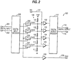
- Figure 2 illustrates a simplified example of a combination 2-bit digital to analog converter sharing references with the 2-bit analog to digital converter shown in Figure 1.
- a converter circuit according to the invention receives an analog input Vin which is applied on input channel 101 to comparators 102-105.
- voltage divider network 106 including resistors 107-111, provides voltage references to comparators 102-105.
- the outputs of the comparators are then encoded by encoder 112 to produce digital outputs 113 and 114.
- Digital inputs are applied, for example, on digital signal lines 201 and 202 to digital input decoder 203.
- Digital input decoder 203 converts the 2-bit digital input into 4 bits which are used to control switches 204-207. For example, logical ones on signal lines 201 and 202 simultaneously would be decoded into logical states such that all four switches 204-207 were closed, thereby applying the maximum possible current to buffer amplifier 208, which would be used to produce Vout on signal line 209. Similarly, logical zeros appearing simultaneously on signal lines 201 and 202 would be decoded such that all four switches 204-207 would be open, thereby producing no current to amplifier 208 and 0 volts at Vout on signal line 209.
- a logical 0 and a logical 1 applied on either of signal lines 201 and 202 would be decoded such that different ones of switches 204-207 would be closed, thereby generating various levels of current to amplifier 208 and various intermediate output voltages on signal line 209. It will be known that the decoding scheme is arbitrary and has been described herein by way of example and not limitation, as any decoding scheme can be implemented to actuate switches 204-207.
- a digital 2-bit to 1-of-4 decoder 203 is used to select which reference voltage already available on voltage divider 106 will be presented to buffer 208 for output.
- the resistive divider is the largest single structure of the flash converter. Using the same divider to provide references for output Vout as for the analog to digital conversion, economizes on silicon area. The converter has the additional benefit of improving accuracy by using the same reference voltages for analog to digital and digital to analog input and output conversions. It will be known to those of ordinary skill that the 2-bit example illustrated in Figure 2 is a simplified example which can be expanded to N-bits as needed.
- FIG. 3 illustrates a timing control system 301 which responds to input requests on signal line 302 and output requests on signal line 303.
- timing control system 301 provides signals 304 and 305 to digital input decoder 203 and digital output encoder 112, respectively.
- Timing control system 301 constrains disturbance of the voltage reference divider 106 to occur only during those times when such disturbances will not affect correct operation of the system.
- timing control system 301 can be constructed using logic devices, processor devices, or programmed devices, such as memories. Timing control system 301 can be configured to inhibit switching of switches 204-207 in response to an input request on signal line 302, or an output request on signal line 303. This is accomplished by transmitting an inhibit signal from timing control system 301 to digital input decoder 203 on signal line 304. Similarly, timing control system 301 can produce an inhibit signal on signal line 305 to prevent digital output encoder 112 from changing state during times when switches 204-207 are changing state. It will be known to those of ordinary skill that timing control system 301 can be implemented to provide enable signals on signal lines 304, 305 as well as inhibit signals.
- timing control system 301 is typically event driven by input and output requests on signal lines 302 and 303, timing control system 301 may also be configured such that inhibit and/or enable signals on signal lines 304 and 305 are generated at particular times relative to a clock.
- the specific configuration of the timing control system 301 will depend on the timing constraints, processing capability and logic family implementation of the system.
- a practical system can be implemented as a 1/n conversion architecture, rather than as the full flash systems shown in Figures 1-3.
- One reason for implementing 1/n flash conversion systems is that as the number of bits of accuracy required increases to higher n, 2 n comparators are required. The number of comparators then begins to dominate the area of silicon chip and increases the power consumption necessary for the system to operate.
- a multi-stage 1/n flash conversion system may include multiplexing and high speed pipelining functions. Multi-stage analog to digital conversion has the effect of adding other potential sources of disturbances to the value of the references.
- each sample may imply that the second 1/2 stage of comparators would be switched to a different set of references at a higher or lower location on the divider.
- the switching operation of the second 1/2 flash stage would disturb values of the reference tree and impose a different set of timing constraints on the timing control circuit in Figure 3.
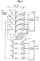
- Figure 4 is a simplified diagram of a 1/2 flash system of 4-bits output accuracy implemented as two 2-bit flashes with 4 comparators for each 2-bits of precision.
- a first 1/2 stage includes comparators 403-406, resistors 413-417, and encoder 418.
- a second 1/2 flash stage includes comparators 407-410, resistors 419-422 and encoder 423.
- switches 401 and 411 are closed, an input signal to be converted is provided on input channel 402 to each of the comparators 403-410.
- the first half flash stage produces logical zeros and ones at the outputs of comparators 403-406.
- switch 411 can be opened.
- switch logic 424 operates to open and close appropriate switches S3-S6 in switch matrix 425. It will be known to those of ordinary skill that switch logic 424 can be implemented within switch matrix 425, although it is shown herein as a separate element in Figure 4 by way of illustration, and not limitation. At this point, outputs B2 and B3 from encoder 418 can be provided to a first in, first out memory to be provided to a system in a pipeline fashion with outputs B1 and B0, which will be generated by the second half flash stage.
- Switching of switch matrix 425 results in the application of a voltage across the network formed by resistors 419-422. This applies voltage references Vref5 through Vref8 to comparators 407-410. The outputs of these comparators are then routed to encoder 423 to provide outputs B1 and B0. These comparator outputs are then also routed to a first-in, first-out memory, not shown, for pipelining to the rest of the system. It will be known to those of ordinary skill that outputs B0-B3 can also be stored and provided in a parallel fashion or transmitted in any other known way for use by the rest of the system.
- voltage references Vref 5 - Vref 8 will be between Vref 1 and Vref 2 when switch S3 is in position a, S4 is in position d, and S5 is in position e and S6 is open.
- voltages Vref 5 - Vref 8 will be between Vref 2 and Vref 3 when switch S3 is open, switch S4 is in position b, switch S5 is in position d, and switch S6 is open.
- Voltage references Vref 5 - Vref 8 will be between Vref 3 and Vref 4 when switch S3 is open, switch S4 is in position c, switch S5 is in position f, and switch S6 is in position g.
- switches S3-S6 is a function of the outputs of comparators 403-406 as determined by switch logic 424. It will also be known to those of ordinary skill that switch matrix 425 can be implemented in any known fashion to apply appropriate voltages at higher or lower levels at a higher or lower location on the divider formed by resistors 413-417 and voltage reference Vref. It will be known to those of ordinary skill that any number of stages for a 1/n flash conversion system can also be formed.
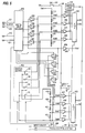
- FIG. 5 shows the incorporation of the digital to analog function with digital input decoder 203 responsive to digital inputs 201-202 and 210-211.
- Digital inputs 201-202 control switching of switches 204-207, while inputs 210-211 control switching of elements 501-504, which are used to provide the higher precision available in the second half flash stage.
- Timing control system 301 is again responsive to input requests on signal line 302 and output requests on signal line 303 to provide enable and inhibit signals on signal lines 304 and 305, as previously discussed.
- timing control system 301 provides enable and inhibit signals to switch matrix 425 to prevent switch matrix 425 from being switched at times when perturbations on voltage references Vref 1 through Vref 8 could produce errors in the output of the converter.
- timing control system 301 operates to control digital input decoder 203, output decoders 418, 423 and switch matrix 425 such that switching of these devices does not occur during input or output requests on signal lines 302, 303.
- FIG. 6 illustrates the 2-input 2-output case with 2-bits of accuracy and a single stage analog to digital converter with digital to analog functions.
- the timing and multiplex control system 601 has the function of steering decoded inputs to the correct set of switches for the channel being output, selecting the correct multiplexer operation so that the desired input channel is converted by the flash analog to digital converter, and assuring that the operation of the various components of the system that might disturb the values of the voltage references generated by the divider are never allowed to occur simultaneously.
- timing and multiplexing control system 601 activates multiplexer 604 to select either Vin a or Vin b .
- the selected input is provided on analog input channel 101 to comparators 102-105 as previously described.
- voltages developed by the voltage divider 106 through resisters 107-111 are applied to the opposite sides of comparators 102-105 to generate a plurality of logical ones and zeros. These logical ones and zeros are encoded by digital output encoder 112 to produce digital outputs on signal lines 113 and 114. Perturbations which occur on the voltage references during this conversion could introduce errors at the digital output.
- timing and multiplexing control system 601 generates an inhibit signal on signal line 605, which prevents switches 606-613 from being activated while such a conversion takes place.
- timing and multiplexing control system 601 When an output request is received on signal lines 614 or 615, timing and multiplexing control system 601 sends a signal on signal lines 605 to digital input decoder 203 to cause appropriate switches among switches 606-613 to be activated. For example, if a signal is received on output request line 615, timing and multiplex control system 601 activates digital input decoder 203 to open and close switches 606, 608, 610 and 612 in response to digital inputs 201 and 202. Similarly, if an output request is received on signal line 614, timing and multiplexing control system 601 activates digital input decoder 203 to open and close switches 607, 609, 611 and 613 in response to digital inputs 201, 202. The result of this switching provides inputs to buffer amplifiers 616 and 617 to produce channelized outputs Vout a and Vout b .
- requests by the various channels can be event generated in an asynchronous fashion or can be scheduled, as for example in a polling circuit.
- Figure 7 illustrates a multi-stage, multi-channel analog to digital converter with digital to analog function according to the invention.
- Figure 7 shows a 1/2 stage flash converter with two channel capability. This converter operates on the same principles as those discussed above for the multi-stage analog to digital converter with digital to analog functions, shown in Figure 5, and the multi-channel analog to digital converter with digital to analog functions, shown in Figure 6.
- Figure 7 illustrates digital input decoder 701 responsive to digital inputs 210 and 211 to control switches 702-709. It will be known to those of ordinary skill that the digital input decoder 701 could be implemented in the same circuitry as digital input decoder 203.
Landscapes
- Engineering & Computer Science (AREA)
- Theoretical Computer Science (AREA)
- Analogue/Digital Conversion (AREA)
Applications Claiming Priority (2)
| Application Number | Priority Date | Filing Date | Title |
|---|---|---|---|
| US114335 | 1987-10-28 | ||
| US08/114,335 US5345234A (en) | 1993-08-31 | 1993-08-31 | Method and apparatus for combining a flash analog to digital converter with digital to analog functions |
Publications (3)
| Publication Number | Publication Date |
|---|---|
| EP0641084A2 true EP0641084A2 (de) | 1995-03-01 |
| EP0641084A3 EP0641084A3 (de) | 1995-11-02 |
| EP0641084B1 EP0641084B1 (de) | 2001-09-12 |
Family
ID=22354627
Family Applications (1)
| Application Number | Title | Priority Date | Filing Date |
|---|---|---|---|
| EP94305472A Expired - Lifetime EP0641084B1 (de) | 1993-08-31 | 1994-07-25 | Analog-digital-analog Umsetzungsschaltung |
Country Status (4)
| Country | Link |
|---|---|
| US (1) | US5345234A (de) |
| EP (1) | EP0641084B1 (de) |
| JP (1) | JPH07154255A (de) |
| DE (1) | DE69428246T2 (de) |
Cited By (1)
| Publication number | Priority date | Publication date | Assignee | Title |
|---|---|---|---|---|
| US6260085B1 (en) | 1997-09-29 | 2001-07-10 | Infineon Technologies Ag | Changeover device which uses both analog and digital signals as input signals and supplies an analog output signal |
Families Citing this family (17)
| Publication number | Priority date | Publication date | Assignee | Title |
|---|---|---|---|---|
| FR2720570B1 (fr) | 1994-05-24 | 1996-08-02 | Thomson Consumer Electronics | Convertisseur A/N de deux signaux analogiques utilisant un seul module convertisseur. |
| US5663728A (en) * | 1995-05-18 | 1997-09-02 | Hughes Aircraft Company | Digital-to-analog converted (DAC) and method that set waveform rise and fall times to produce an analog waveform that approximates a piecewise linear waveform to reduce spectral distortion |
| JPH0968721A (ja) * | 1995-08-31 | 1997-03-11 | Sharp Corp | 液晶表示素子 |
| US5651037A (en) * | 1995-10-04 | 1997-07-22 | Motorola, Inc. | Apparatus for preforming discrete-time analog queuing and computing in a communication system |
| KR100515797B1 (ko) * | 1997-03-21 | 2005-12-14 | 코닌클리즈케 필립스 일렉트로닉스 엔.브이. | 신호처리시스템및그것의신호처리방법 |
| US5864310A (en) * | 1997-03-21 | 1999-01-26 | Philips Electronics North America Corporation | Wireless receiver with offset compensation using flash-ADC |
| KR19990018936A (ko) * | 1997-08-28 | 1999-03-15 | 윤종용 | 아날로그-디지탈 변환 회로 |
| FR2798020A1 (fr) * | 1999-08-31 | 2001-03-02 | Koninkl Philips Electronics Nv | Procede d'encodage binaire/thermometrique simplifie a resolution amelioree |
| KR20050017914A (ko) * | 2003-08-11 | 2005-02-23 | 학교법인 포항공과대학교 | 단일 입력 단의 씨모스 타임 인터리브드 플래쉬아날로그/디지털 변환장치 |
| US7443326B2 (en) * | 2003-10-27 | 2008-10-28 | Dan Raphaeli | Digital input signals constructor providing analog representation thereof |
| GB0622199D0 (en) * | 2006-11-07 | 2006-12-20 | Cambridge Silicon Radio Ltd | Rail to rail flash |
| KR101082415B1 (ko) * | 2007-07-24 | 2011-11-11 | 고려대학교 산학협력단 | 계층구조 위상 디지털 변환기 |
| GB0907382D0 (en) * | 2009-04-29 | 2009-06-10 | Cambridge Silicon Radio Ltd | High speed low voltage flash |
| US9136852B2 (en) * | 2011-12-26 | 2015-09-15 | Qixing Chen | Multi-stage parallel super-high-speed ADC and DAC of logarithmic companding law |
| RU175095U1 (ru) * | 2015-01-12 | 2017-11-20 | федеральное государственное бюджетное образовательное учреждение высшего образования "Российский государственный гидрометеорологический университет" | Многофункциональный аналого-цифро-аналоговый элемент |
| FR3059455B1 (fr) * | 2016-11-29 | 2020-09-25 | Continental Automotive France | Procede et dispositif de detection de presence pour vehicule automobile |
| US10425095B1 (en) * | 2018-08-27 | 2019-09-24 | Qualcomm Incorporated | Multiple-bit parallel successive approximation (SA) flash analog-to-digital converter (ADC) circuits |
Family Cites Families (8)
| Publication number | Priority date | Publication date | Assignee | Title |
|---|---|---|---|---|
| US4160243A (en) * | 1976-09-28 | 1979-07-03 | Fujitsu Limited | Asynchronous reversible analog to digital converter |
| JPS56162534A (en) * | 1980-05-19 | 1981-12-14 | Nec Corp | Analog-to-digital and digital-to-analog converter circuit |
| US4745393A (en) * | 1985-09-25 | 1988-05-17 | Hitachi, Ltd | Analog-to-digital converter |
| JPH0754910B2 (ja) * | 1986-03-10 | 1995-06-07 | 株式会社日立製作所 | Ad変換器 |
| US4857931A (en) * | 1987-07-20 | 1989-08-15 | Zdzislaw Gulczynski | Dual flash analog-to-digital converter |
| FR2652689A1 (fr) * | 1989-10-02 | 1991-04-05 | France Etat | Convertisseur analogique/numerique a haute frequence de conversion. |
| JPH03237821A (ja) * | 1990-02-15 | 1991-10-23 | Canon Inc | 信号変換装置 |
| US5111205A (en) * | 1990-12-18 | 1992-05-05 | Vlsi Technology, Inc. | Digital-to-analog and analog-to-digital converters |
-
1993
- 1993-08-31 US US08/114,335 patent/US5345234A/en not_active Expired - Lifetime
-
1994
- 1994-07-25 EP EP94305472A patent/EP0641084B1/de not_active Expired - Lifetime
- 1994-07-25 DE DE69428246T patent/DE69428246T2/de not_active Expired - Fee Related
- 1994-08-30 JP JP6204857A patent/JPH07154255A/ja not_active Withdrawn
Cited By (1)
| Publication number | Priority date | Publication date | Assignee | Title |
|---|---|---|---|---|
| US6260085B1 (en) | 1997-09-29 | 2001-07-10 | Infineon Technologies Ag | Changeover device which uses both analog and digital signals as input signals and supplies an analog output signal |
Also Published As
| Publication number | Publication date |
|---|---|
| DE69428246T2 (de) | 2002-06-13 |
| EP0641084B1 (de) | 2001-09-12 |
| US5345234A (en) | 1994-09-06 |
| JPH07154255A (ja) | 1995-06-16 |
| DE69428246D1 (de) | 2001-10-18 |
| EP0641084A3 (de) | 1995-11-02 |
Similar Documents
| Publication | Publication Date | Title |
|---|---|---|
| US5345234A (en) | Method and apparatus for combining a flash analog to digital converter with digital to analog functions | |
| US5450085A (en) | Method and apparatus for high speed analog to digital conversion using multiplexed flash sections | |
| KR100318441B1 (ko) | 아날로그-디지털변환장치및그변환방법 | |
| US6081219A (en) | Power saving arrangement for a flash A/D converter | |
| US6762707B2 (en) | Programmable architecture analog-to-digital converter | |
| US5130578A (en) | Efficient high speed N-word comparator | |
| US6094154A (en) | Analog-to-digital converter | |
| US4202042A (en) | Digital to analog interface for simultaneous analog outputs | |
| US4381498A (en) | Analog-to-digital converting apparatus | |
| JPH11154866A (ja) | 逐次比較型ad変換器 | |
| EP0681372A1 (de) | Schaltung zur Digital-/Analogumsetzung und die Schaltung benutzender AD-Wandler | |
| US6927723B2 (en) | A/D converter and A/D conversion method | |
| US20040017305A1 (en) | A/D conversion method for serial/parallel A/D converter, and serial/parallel A/D converter | |
| US6127959A (en) | Flash analog-to-digital converter with reduced number of resistors and comparators | |
| US4857930A (en) | Circuit for reducing differential nonlinearities in multi-stage digital-to-analog converters | |
| JP2001148631A (ja) | アナログ・ディジタル変換器、マイクロコンピュータおよびアナログ・ディジタル変換方法 | |
| US20040189504A1 (en) | Semi-flash A/D converter with minimal comparator count | |
| JPS6373718A (ja) | R−2r型d/aコンバ−タ回路 | |
| US5410312A (en) | Digital/analog conversion device with two switched latches for simultaneous D/A conversion | |
| US4864304A (en) | Analog voltage signal comparator circuit | |
| US5684483A (en) | Floating point digital to analog converter | |
| KR100261997B1 (ko) | 아날로그-디지탈 변환기 | |
| KR100339542B1 (ko) | 고속 아날로그/디지털 변환기 | |
| KR100678786B1 (ko) | 이진 워드의 써모메트릭 신호로의 변환 방법, 이진 입력 워드를 수신하여 써모메트릭 신호를 제공하는 써모메트릭 인코더 및 디지털 입력 신호를 아날로그 출력 신호로 변환하는 변환 장치 | |
| CN115940945A (zh) | 一种单通道单adc模数转换器采样精度增倍的电路 |
Legal Events
| Date | Code | Title | Description |
|---|---|---|---|
| PUAI | Public reference made under article 153(3) epc to a published international application that has entered the european phase |
Free format text: ORIGINAL CODE: 0009012 |
|
| AK | Designated contracting states |
Kind code of ref document: A2 Designated state(s): BE DE DK ES FR GB GR IE IT LU NL PT SE |
|
| PUAL | Search report despatched |
Free format text: ORIGINAL CODE: 0009013 |
|
| AK | Designated contracting states |
Kind code of ref document: A3 Designated state(s): BE DE DK ES FR GB GR IE IT LU NL PT SE |
|
| 17P | Request for examination filed |
Effective date: 19960205 |
|
| 17Q | First examination report despatched |
Effective date: 19980702 |
|
| GRAG | Despatch of communication of intention to grant |
Free format text: ORIGINAL CODE: EPIDOS AGRA |
|
| GRAG | Despatch of communication of intention to grant |
Free format text: ORIGINAL CODE: EPIDOS AGRA |
|
| GRAH | Despatch of communication of intention to grant a patent |
Free format text: ORIGINAL CODE: EPIDOS IGRA |
|
| GRAH | Despatch of communication of intention to grant a patent |
Free format text: ORIGINAL CODE: EPIDOS IGRA |
|
| GRAA | (expected) grant |
Free format text: ORIGINAL CODE: 0009210 |
|
| AK | Designated contracting states |
Kind code of ref document: B1 Designated state(s): BE DE DK ES FR GB GR IE IT LU NL PT SE |
|
| PG25 | Lapsed in a contracting state [announced via postgrant information from national office to epo] |
Ref country code: NL Free format text: LAPSE BECAUSE OF FAILURE TO SUBMIT A TRANSLATION OF THE DESCRIPTION OR TO PAY THE FEE WITHIN THE PRESCRIBED TIME-LIMIT Effective date: 20010912 Ref country code: IT Free format text: LAPSE BECAUSE OF FAILURE TO SUBMIT A TRANSLATION OF THE DESCRIPTION OR TO PAY THE FEE WITHIN THE PRESCRIBED TIME-LIMIT;WARNING: LAPSES OF ITALIAN PATENTS WITH EFFECTIVE DATE BEFORE 2007 MAY HAVE OCCURRED AT ANY TIME BEFORE 2007. THE CORRECT EFFECTIVE DATE MAY BE DIFFERENT FROM THE ONE RECORDED. Effective date: 20010912 Ref country code: FR Free format text: LAPSE BECAUSE OF FAILURE TO SUBMIT A TRANSLATION OF THE DESCRIPTION OR TO PAY THE FEE WITHIN THE PRESCRIBED TIME-LIMIT Effective date: 20010912 Ref country code: BE Free format text: LAPSE BECAUSE OF FAILURE TO SUBMIT A TRANSLATION OF THE DESCRIPTION OR TO PAY THE FEE WITHIN THE PRESCRIBED TIME-LIMIT Effective date: 20010912 |
|
| REG | Reference to a national code |
Ref country code: IE Ref legal event code: FG4D |
|
| REF | Corresponds to: |
Ref document number: 69428246 Country of ref document: DE Date of ref document: 20011018 |
|
| PG25 | Lapsed in a contracting state [announced via postgrant information from national office to epo] |
Ref country code: SE Free format text: LAPSE BECAUSE OF FAILURE TO SUBMIT A TRANSLATION OF THE DESCRIPTION OR TO PAY THE FEE WITHIN THE PRESCRIBED TIME-LIMIT Effective date: 20011212 Ref country code: PT Free format text: LAPSE BECAUSE OF FAILURE TO SUBMIT A TRANSLATION OF THE DESCRIPTION OR TO PAY THE FEE WITHIN THE PRESCRIBED TIME-LIMIT Effective date: 20011212 Ref country code: DK Free format text: LAPSE BECAUSE OF FAILURE TO SUBMIT A TRANSLATION OF THE DESCRIPTION OR TO PAY THE FEE WITHIN THE PRESCRIBED TIME-LIMIT Effective date: 20011212 |
|
| PG25 | Lapsed in a contracting state [announced via postgrant information from national office to epo] |
Ref country code: GR Free format text: LAPSE BECAUSE OF FAILURE TO SUBMIT A TRANSLATION OF THE DESCRIPTION OR TO PAY THE FEE WITHIN THE PRESCRIBED TIME-LIMIT Effective date: 20011214 |
|
| REG | Reference to a national code |
Ref country code: GB Ref legal event code: IF02 |
|
| NLV1 | Nl: lapsed or annulled due to failure to fulfill the requirements of art. 29p and 29m of the patents act | ||
| PG25 | Lapsed in a contracting state [announced via postgrant information from national office to epo] |
Ref country code: ES Free format text: LAPSE BECAUSE OF FAILURE TO SUBMIT A TRANSLATION OF THE DESCRIPTION OR TO PAY THE FEE WITHIN THE PRESCRIBED TIME-LIMIT Effective date: 20020326 |
|
| PGFP | Annual fee paid to national office [announced via postgrant information from national office to epo] |
Ref country code: GB Payment date: 20020613 Year of fee payment: 9 |
|
| PLBE | No opposition filed within time limit |
Free format text: ORIGINAL CODE: 0009261 |
|
| STAA | Information on the status of an ep patent application or granted ep patent |
Free format text: STATUS: NO OPPOSITION FILED WITHIN TIME LIMIT |
|
| PG25 | Lapsed in a contracting state [announced via postgrant information from national office to epo] |
Ref country code: LU Free format text: LAPSE BECAUSE OF NON-PAYMENT OF DUE FEES Effective date: 20020725 Ref country code: IE Free format text: LAPSE BECAUSE OF NON-PAYMENT OF DUE FEES Effective date: 20020725 |
|
| EN | Fr: translation not filed | ||
| 26N | No opposition filed | ||
| REG | Reference to a national code |
Ref country code: IE Ref legal event code: MM4A |
|
| PG25 | Lapsed in a contracting state [announced via postgrant information from national office to epo] |
Ref country code: GB Free format text: LAPSE BECAUSE OF NON-PAYMENT OF DUE FEES Effective date: 20030725 |
|
| GBPC | Gb: european patent ceased through non-payment of renewal fee |
Effective date: 20030725 |
|
| PGFP | Annual fee paid to national office [announced via postgrant information from national office to epo] |
Ref country code: DE Payment date: 20070731 Year of fee payment: 14 |
|
| PG25 | Lapsed in a contracting state [announced via postgrant information from national office to epo] |
Ref country code: DE Free format text: LAPSE BECAUSE OF NON-PAYMENT OF DUE FEES Effective date: 20090203 |