EP0623940B1 - Condensateur céramique multicouche sous forme de puce et son procédé de fabrication - Google Patents
Condensateur céramique multicouche sous forme de puce et son procédé de fabrication Download PDFInfo
- Publication number
- EP0623940B1 EP0623940B1 EP94112039A EP94112039A EP0623940B1 EP 0623940 B1 EP0623940 B1 EP 0623940B1 EP 94112039 A EP94112039 A EP 94112039A EP 94112039 A EP94112039 A EP 94112039A EP 0623940 B1 EP0623940 B1 EP 0623940B1
- Authority
- EP
- European Patent Office
- Prior art keywords
- oxide
- capacitor
- weight
- layer
- dielectric
- Prior art date
- Legal status (The legal status is an assumption and is not a legal conclusion. Google has not performed a legal analysis and makes no representation as to the accuracy of the status listed.)
- Expired - Lifetime
Links
- 239000003990 capacitor Substances 0.000 title claims description 96
- 238000000034 method Methods 0.000 title claims description 26
- 239000000919 ceramic Substances 0.000 title claims description 20
- VYPSYNLAJGMNEJ-UHFFFAOYSA-N Silicium dioxide Chemical compound O=[Si]=O VYPSYNLAJGMNEJ-UHFFFAOYSA-N 0.000 claims description 107
- 239000000203 mixture Substances 0.000 claims description 74
- DLYUQMMRRRQYAE-UHFFFAOYSA-N tetraphosphorus decaoxide Chemical compound O1P(O2)(=O)OP3(=O)OP1(=O)OP2(=O)O3 DLYUQMMRRRQYAE-UHFFFAOYSA-N 0.000 claims description 72
- PXHVJJICTQNCMI-UHFFFAOYSA-N Nickel Chemical compound [Ni] PXHVJJICTQNCMI-UHFFFAOYSA-N 0.000 claims description 65
- 238000010304 firing Methods 0.000 claims description 50
- 229910052681 coesite Inorganic materials 0.000 claims description 49
- 229910052906 cristobalite Inorganic materials 0.000 claims description 49
- 239000003989 dielectric material Substances 0.000 claims description 49
- 239000000377 silicon dioxide Substances 0.000 claims description 49
- 229910052682 stishovite Inorganic materials 0.000 claims description 49
- 229910052905 tridymite Inorganic materials 0.000 claims description 49
- QVGXLLKOCUKJST-UHFFFAOYSA-N atomic oxygen Chemical compound [O] QVGXLLKOCUKJST-UHFFFAOYSA-N 0.000 claims description 48
- 239000001301 oxygen Substances 0.000 claims description 48
- 229910052760 oxygen Inorganic materials 0.000 claims description 48
- AMWRITDGCCNYAT-UHFFFAOYSA-L hydroxy(oxo)manganese;manganese Chemical compound [Mn].O[Mn]=O.O[Mn]=O AMWRITDGCCNYAT-UHFFFAOYSA-L 0.000 claims description 35
- PNEYBMLMFCGWSK-UHFFFAOYSA-N aluminium oxide Inorganic materials [O-2].[O-2].[O-2].[Al+3].[Al+3] PNEYBMLMFCGWSK-UHFFFAOYSA-N 0.000 claims description 33
- 229910052593 corundum Inorganic materials 0.000 claims description 30
- 229910001845 yogo sapphire Inorganic materials 0.000 claims description 30
- JEIPFZHSYJVQDO-UHFFFAOYSA-N iron(III) oxide Inorganic materials O=[Fe]O[Fe]=O JEIPFZHSYJVQDO-UHFFFAOYSA-N 0.000 claims description 28
- 239000000463 material Substances 0.000 claims description 25
- 229910052759 nickel Inorganic materials 0.000 claims description 21
- 229910000990 Ni alloy Inorganic materials 0.000 claims description 16
- 229910052698 phosphorus Inorganic materials 0.000 claims description 16
- 229910052726 zirconium Inorganic materials 0.000 claims description 16
- FUJCRWPEOMXPAD-UHFFFAOYSA-N lithium oxide Chemical compound [Li+].[Li+].[O-2] FUJCRWPEOMXPAD-UHFFFAOYSA-N 0.000 claims description 14
- UQSXHKLRYXJYBZ-UHFFFAOYSA-N Iron oxide Chemical compound [Fe]=O UQSXHKLRYXJYBZ-UHFFFAOYSA-N 0.000 claims description 13
- 229910001392 phosphorus oxide Inorganic materials 0.000 claims description 12
- 150000001875 compounds Chemical class 0.000 claims description 11
- 229910052814 silicon oxide Inorganic materials 0.000 claims description 10
- 229910001947 lithium oxide Inorganic materials 0.000 claims description 9
- VSAISIQCTGDGPU-UHFFFAOYSA-N tetraphosphorus hexaoxide Chemical compound O1P(O2)OP3OP1OP2O3 VSAISIQCTGDGPU-UHFFFAOYSA-N 0.000 claims description 9
- 229910052718 tin Inorganic materials 0.000 claims description 6
- 229910052692 Dysprosium Inorganic materials 0.000 claims description 5
- 229910052688 Gadolinium Inorganic materials 0.000 claims description 5
- 229910052771 Terbium Inorganic materials 0.000 claims description 5
- 229910052716 thallium Inorganic materials 0.000 claims description 5
- 229910052727 yttrium Inorganic materials 0.000 claims description 5
- 229910052725 zinc Inorganic materials 0.000 claims description 5
- 229910052793 cadmium Inorganic materials 0.000 claims description 4
- 229910052750 molybdenum Inorganic materials 0.000 claims description 4
- 229910052720 vanadium Inorganic materials 0.000 claims description 4
- 150000002642 lithium compounds Chemical class 0.000 claims description 2
- BHEPBYXIRTUNPN-UHFFFAOYSA-N hydridophosphorus(.) (triplet) Chemical compound [PH] BHEPBYXIRTUNPN-UHFFFAOYSA-N 0.000 claims 1
- 239000010410 layer Substances 0.000 description 168
- GWEVSGVZZGPLCZ-UHFFFAOYSA-N Titan oxide Chemical compound O=[Ti]=O GWEVSGVZZGPLCZ-UHFFFAOYSA-N 0.000 description 62
- 239000010936 titanium Substances 0.000 description 53
- MCMNRKCIXSYSNV-UHFFFAOYSA-N Zirconium dioxide Chemical compound O=[Zr]=O MCMNRKCIXSYSNV-UHFFFAOYSA-N 0.000 description 50
- 239000011572 manganese Substances 0.000 description 49
- 238000010438 heat treatment Methods 0.000 description 45
- 239000012298 atmosphere Substances 0.000 description 38
- 239000007789 gas Substances 0.000 description 37
- XEEYBQQBJWHFJM-UHFFFAOYSA-N iron Substances [Fe] XEEYBQQBJWHFJM-UHFFFAOYSA-N 0.000 description 37
- 238000001816 cooling Methods 0.000 description 32
- 238000004458 analytical method Methods 0.000 description 22
- 239000002245 particle Substances 0.000 description 22
- 239000000654 additive Substances 0.000 description 20
- GNTDGMZSJNCJKK-UHFFFAOYSA-N divanadium pentaoxide Chemical compound O=[V](=O)O[V](=O)=O GNTDGMZSJNCJKK-UHFFFAOYSA-N 0.000 description 20
- 239000000843 powder Substances 0.000 description 17
- 230000000996 additive effect Effects 0.000 description 16
- 239000011230 binding agent Substances 0.000 description 16
- 238000012360 testing method Methods 0.000 description 15
- 229910052748 manganese Inorganic materials 0.000 description 14
- 239000002243 precursor Substances 0.000 description 13
- 229910052719 titanium Inorganic materials 0.000 description 11
- 229910052782 aluminium Inorganic materials 0.000 description 10
- 229910052791 calcium Inorganic materials 0.000 description 10
- YXFVVABEGXRONW-UHFFFAOYSA-N Toluene Chemical compound CC1=CC=CC=C1 YXFVVABEGXRONW-UHFFFAOYSA-N 0.000 description 9
- 239000004615 ingredient Substances 0.000 description 9
- XLOMVQKBTHCTTD-UHFFFAOYSA-N Zinc monoxide Chemical compound [Zn]=O XLOMVQKBTHCTTD-UHFFFAOYSA-N 0.000 description 8
- 229910052788 barium Inorganic materials 0.000 description 8
- JKQOBWVOAYFWKG-UHFFFAOYSA-N molybdenum trioxide Chemical compound O=[Mo](=O)=O JKQOBWVOAYFWKG-UHFFFAOYSA-N 0.000 description 8
- 229910052710 silicon Inorganic materials 0.000 description 8
- XOLBLPGZBRYERU-UHFFFAOYSA-N tin dioxide Chemical compound O=[Sn]=O XOLBLPGZBRYERU-UHFFFAOYSA-N 0.000 description 8
- IJGRMHOSHXDMSA-UHFFFAOYSA-N Atomic nitrogen Chemical compound N#N IJGRMHOSHXDMSA-UHFFFAOYSA-N 0.000 description 7
- 229910002113 barium titanate Inorganic materials 0.000 description 7
- 230000008901 benefit Effects 0.000 description 7
- 239000002131 composite material Substances 0.000 description 7
- 239000002270 dispersing agent Substances 0.000 description 7
- 239000012535 impurity Substances 0.000 description 7
- KDLHZDBZIXYQEI-UHFFFAOYSA-N Palladium Chemical compound [Pd] KDLHZDBZIXYQEI-UHFFFAOYSA-N 0.000 description 6
- -1 Tb2O3 Inorganic materials 0.000 description 6
- RTAQQCXQSZGOHL-UHFFFAOYSA-N Titanium Chemical compound [Ti] RTAQQCXQSZGOHL-UHFFFAOYSA-N 0.000 description 6
- WUOACPNHFRMFPN-UHFFFAOYSA-N alpha-terpineol Chemical compound CC1=CCC(C(C)(C)O)CC1 WUOACPNHFRMFPN-UHFFFAOYSA-N 0.000 description 6
- JRPBQTZRNDNNOP-UHFFFAOYSA-N barium titanate Chemical compound [Ba+2].[Ba+2].[O-][Ti]([O-])([O-])[O-] JRPBQTZRNDNNOP-UHFFFAOYSA-N 0.000 description 6
- SQIFACVGCPWBQZ-UHFFFAOYSA-N delta-terpineol Natural products CC(C)(O)C1CCC(=C)CC1 SQIFACVGCPWBQZ-UHFFFAOYSA-N 0.000 description 6
- 229910052742 iron Inorganic materials 0.000 description 6
- 235000013980 iron oxide Nutrition 0.000 description 6
- 238000004519 manufacturing process Methods 0.000 description 6
- 239000002904 solvent Substances 0.000 description 6
- 229940116411 terpineol Drugs 0.000 description 6
- XUCJHNOBJLKZNU-UHFFFAOYSA-M dilithium;hydroxide Chemical compound [Li+].[Li+].[OH-] XUCJHNOBJLKZNU-UHFFFAOYSA-M 0.000 description 5
- 238000002156 mixing Methods 0.000 description 5
- 238000007254 oxidation reaction Methods 0.000 description 5
- 239000002002 slurry Substances 0.000 description 5
- VTYYLEPIZMXCLO-UHFFFAOYSA-L Calcium carbonate Chemical compound [Ca+2].[O-]C([O-])=O VTYYLEPIZMXCLO-UHFFFAOYSA-L 0.000 description 4
- 229910008649 Tl2O3 Inorganic materials 0.000 description 4
- 239000003570 air Substances 0.000 description 4
- 239000000956 alloy Substances 0.000 description 4
- AYJRCSIUFZENHW-UHFFFAOYSA-L barium carbonate Chemical compound [Ba+2].[O-]C([O-])=O AYJRCSIUFZENHW-UHFFFAOYSA-L 0.000 description 4
- CXKCTMHTOKXKQT-UHFFFAOYSA-N cadmium oxide Inorganic materials [Cd]=O CXKCTMHTOKXKQT-UHFFFAOYSA-N 0.000 description 4
- 230000000052 comparative effect Effects 0.000 description 4
- 239000004020 conductor Substances 0.000 description 4
- DOIRQSBPFJWKBE-UHFFFAOYSA-N dibutyl phthalate Chemical compound CCCCOC(=O)C1=CC=CC=C1C(=O)OCCCC DOIRQSBPFJWKBE-UHFFFAOYSA-N 0.000 description 4
- NLQFUUYNQFMIJW-UHFFFAOYSA-N dysprosium(III) oxide Inorganic materials O=[Dy]O[Dy]=O NLQFUUYNQFMIJW-UHFFFAOYSA-N 0.000 description 4
- CMIHHWBVHJVIGI-UHFFFAOYSA-N gadolinium(III) oxide Inorganic materials [O-2].[O-2].[O-2].[Gd+3].[Gd+3] CMIHHWBVHJVIGI-UHFFFAOYSA-N 0.000 description 4
- QTQRFJQXXUPYDI-UHFFFAOYSA-N oxo(oxothallanyloxy)thallane Chemical compound O=[Tl]O[Tl]=O QTQRFJQXXUPYDI-UHFFFAOYSA-N 0.000 description 4
- 239000004014 plasticizer Substances 0.000 description 4
- RUDFQVOCFDJEEF-UHFFFAOYSA-N yttrium(III) oxide Inorganic materials [O-2].[O-2].[O-2].[Y+3].[Y+3] RUDFQVOCFDJEEF-UHFFFAOYSA-N 0.000 description 4
- ZWEHNKRNPOVVGH-UHFFFAOYSA-N 2-Butanone Chemical compound CCC(C)=O ZWEHNKRNPOVVGH-UHFFFAOYSA-N 0.000 description 3
- 239000001856 Ethyl cellulose Substances 0.000 description 3
- ZZSNKZQZMQGXPY-UHFFFAOYSA-N Ethyl cellulose Chemical compound CCOCC1OC(OC)C(OCC)C(OCC)C1OC1C(O)C(O)C(OC)C(CO)O1 ZZSNKZQZMQGXPY-UHFFFAOYSA-N 0.000 description 3
- PEDCQBHIVMGVHV-UHFFFAOYSA-N Glycerine Chemical compound OCC(O)CO PEDCQBHIVMGVHV-UHFFFAOYSA-N 0.000 description 3
- PWHULOQIROXLJO-UHFFFAOYSA-N Manganese Chemical compound [Mn] PWHULOQIROXLJO-UHFFFAOYSA-N 0.000 description 3
- 229910045601 alloy Inorganic materials 0.000 description 3
- 238000001354 calcination Methods 0.000 description 3
- 239000011575 calcium Substances 0.000 description 3
- 229910001873 dinitrogen Inorganic materials 0.000 description 3
- 238000009826 distribution Methods 0.000 description 3
- 238000000635 electron micrograph Methods 0.000 description 3
- 235000019325 ethyl cellulose Nutrition 0.000 description 3
- 229920001249 ethyl cellulose Polymers 0.000 description 3
- 239000011521 glass Substances 0.000 description 3
- 238000009413 insulation Methods 0.000 description 3
- 238000004898 kneading Methods 0.000 description 3
- 239000004922 lacquer Substances 0.000 description 3
- 239000011656 manganese carbonate Substances 0.000 description 3
- 229910000016 manganese(II) carbonate Inorganic materials 0.000 description 3
- 238000004452 microanalysis Methods 0.000 description 3
- 238000001000 micrograph Methods 0.000 description 3
- 239000012299 nitrogen atmosphere Substances 0.000 description 3
- 150000002902 organometallic compounds Chemical class 0.000 description 3
- 230000003647 oxidation Effects 0.000 description 3
- LFGREXWGYUGZLY-UHFFFAOYSA-N phosphoryl Chemical class [P]=O LFGREXWGYUGZLY-UHFFFAOYSA-N 0.000 description 3
- 238000005488 sandblasting Methods 0.000 description 3
- 238000005245 sintering Methods 0.000 description 3
- 239000007921 spray Substances 0.000 description 3
- 229910052712 strontium Inorganic materials 0.000 description 3
- XLYOFNOQVPJJNP-UHFFFAOYSA-N water Substances O XLYOFNOQVPJJNP-UHFFFAOYSA-N 0.000 description 3
- RSWGJHLUYNHPMX-OZNCTZQZSA-N (1r)-1,4a-dimethyl-7-propan-2-yl-2,3,4,4b,5,6,10,10a-octahydrophenanthrene-1-carboxylic acid Chemical compound C12CCC(C(C)C)=CC2=CCC2C1(C)CCC[C@@]2(C)C(O)=O RSWGJHLUYNHPMX-OZNCTZQZSA-N 0.000 description 2
- OAYXUHPQHDHDDZ-UHFFFAOYSA-N 2-(2-butoxyethoxy)ethanol Chemical compound CCCCOCCOCCO OAYXUHPQHDHDDZ-UHFFFAOYSA-N 0.000 description 2
- 229910000807 Ga alloy Inorganic materials 0.000 description 2
- UFHFLCQGNIYNRP-UHFFFAOYSA-N Hydrogen Chemical compound [H][H] UFHFLCQGNIYNRP-UHFFFAOYSA-N 0.000 description 2
- 229910001252 Pd alloy Inorganic materials 0.000 description 2
- 230000015572 biosynthetic process Effects 0.000 description 2
- 229910000019 calcium carbonate Inorganic materials 0.000 description 2
- 150000004649 carbonic acid derivatives Chemical class 0.000 description 2
- 230000015556 catabolic process Effects 0.000 description 2
- 229910052802 copper Inorganic materials 0.000 description 2
- 238000005520 cutting process Methods 0.000 description 2
- 235000014113 dietary fatty acids Nutrition 0.000 description 2
- 239000000194 fatty acid Substances 0.000 description 2
- 229930195729 fatty acid Natural products 0.000 description 2
- 235000011187 glycerol Nutrition 0.000 description 2
- 239000001257 hydrogen Substances 0.000 description 2
- 229910052739 hydrogen Inorganic materials 0.000 description 2
- 150000002697 manganese compounds Chemical class 0.000 description 2
- NUJOXMJBOLGQSY-UHFFFAOYSA-N manganese dioxide Chemical compound O=[Mn]=O NUJOXMJBOLGQSY-UHFFFAOYSA-N 0.000 description 2
- PPNAOCWZXJOHFK-UHFFFAOYSA-N manganese(2+);oxygen(2-) Chemical class [O-2].[Mn+2] PPNAOCWZXJOHFK-UHFFFAOYSA-N 0.000 description 2
- 229910052751 metal Inorganic materials 0.000 description 2
- 239000002184 metal Substances 0.000 description 2
- 230000004048 modification Effects 0.000 description 2
- 238000012986 modification Methods 0.000 description 2
- 150000002823 nitrates Chemical class 0.000 description 2
- 229910052757 nitrogen Inorganic materials 0.000 description 2
- 150000003901 oxalic acid esters Chemical class 0.000 description 2
- 229910052763 palladium Inorganic materials 0.000 description 2
- 229920002037 poly(vinyl butyral) polymer Polymers 0.000 description 2
- 239000010703 silicon Substances 0.000 description 2
- 229910052709 silver Inorganic materials 0.000 description 2
- 239000002356 single layer Substances 0.000 description 2
- 239000000126 substance Substances 0.000 description 2
- 150000003467 sulfuric acid derivatives Chemical class 0.000 description 2
- OGIDPMRJRNCKJF-UHFFFAOYSA-N titanium oxide Inorganic materials [Ti]=O OGIDPMRJRNCKJF-UHFFFAOYSA-N 0.000 description 2
- WRIDQFICGBMAFQ-UHFFFAOYSA-N (E)-8-Octadecenoic acid Natural products CCCCCCCCCC=CCCCCCCC(O)=O WRIDQFICGBMAFQ-UHFFFAOYSA-N 0.000 description 1
- QTYUSOHYEPOHLV-FNORWQNLSA-N 1,3-Octadiene Chemical compound CCCC\C=C\C=C QTYUSOHYEPOHLV-FNORWQNLSA-N 0.000 description 1
- RZRNAYUHWVFMIP-KTKRTIGZSA-N 1-oleoylglycerol Chemical compound CCCCCCCC\C=C/CCCCCCCC(=O)OCC(O)CO RZRNAYUHWVFMIP-KTKRTIGZSA-N 0.000 description 1
- LQJBNNIYVWPHFW-UHFFFAOYSA-N 20:1omega9c fatty acid Natural products CCCCCCCCCCC=CCCCCCCCC(O)=O LQJBNNIYVWPHFW-UHFFFAOYSA-N 0.000 description 1
- QSBYPNXLFMSGKH-UHFFFAOYSA-N 9-Heptadecensaeure Natural products CCCCCCCC=CCCCCCCCC(O)=O QSBYPNXLFMSGKH-UHFFFAOYSA-N 0.000 description 1
- 229920000178 Acrylic resin Polymers 0.000 description 1
- 239000004925 Acrylic resin Substances 0.000 description 1
- 241000273930 Brevoortia tyrannus Species 0.000 description 1
- 229910002971 CaTiO3 Inorganic materials 0.000 description 1
- 229910000881 Cu alloy Inorganic materials 0.000 description 1
- QPLDLSVMHZLSFG-UHFFFAOYSA-N CuO Inorganic materials [Cu]=O QPLDLSVMHZLSFG-UHFFFAOYSA-N 0.000 description 1
- MQIUGAXCHLFZKX-UHFFFAOYSA-N Di-n-octyl phthalate Natural products CCCCCCCCOC(=O)C1=CC=CC=C1C(=O)OCCCCCCCC MQIUGAXCHLFZKX-UHFFFAOYSA-N 0.000 description 1
- LVGKNOAMLMIIKO-UHFFFAOYSA-N Elaidinsaeure-aethylester Natural products CCCCCCCCC=CCCCCCCCC(=O)OCC LVGKNOAMLMIIKO-UHFFFAOYSA-N 0.000 description 1
- 229910017676 MgTiO3 Inorganic materials 0.000 description 1
- 229910002651 NO3 Inorganic materials 0.000 description 1
- NHNBFGGVMKEFGY-UHFFFAOYSA-N Nitrate Chemical compound [O-][N+]([O-])=O NHNBFGGVMKEFGY-UHFFFAOYSA-N 0.000 description 1
- REYJJPSVUYRZGE-UHFFFAOYSA-N Octadecylamine Chemical compound CCCCCCCCCCCCCCCCCCN REYJJPSVUYRZGE-UHFFFAOYSA-N 0.000 description 1
- 239000005642 Oleic acid Substances 0.000 description 1
- ZQPPMHVWECSIRJ-UHFFFAOYSA-N Oleic acid Natural products CCCCCCCCC=CCCCCCCCC(O)=O ZQPPMHVWECSIRJ-UHFFFAOYSA-N 0.000 description 1
- MUBZPKHOEPUJKR-UHFFFAOYSA-N Oxalic acid Chemical compound OC(=O)C(O)=O MUBZPKHOEPUJKR-UHFFFAOYSA-N 0.000 description 1
- NBIIXXVUZAFLBC-UHFFFAOYSA-N Phosphoric acid Chemical group OP(O)(O)=O NBIIXXVUZAFLBC-UHFFFAOYSA-N 0.000 description 1
- 239000002202 Polyethylene glycol Substances 0.000 description 1
- 229910002370 SrTiO3 Inorganic materials 0.000 description 1
- QAOWNCQODCNURD-UHFFFAOYSA-L Sulfate Chemical compound [O-]S([O-])(=O)=O QAOWNCQODCNURD-UHFFFAOYSA-L 0.000 description 1
- ATJFFYVFTNAWJD-UHFFFAOYSA-N Tin Chemical compound [Sn] ATJFFYVFTNAWJD-UHFFFAOYSA-N 0.000 description 1
- 230000002159 abnormal effect Effects 0.000 description 1
- 230000002411 adverse Effects 0.000 description 1
- 239000012080 ambient air Substances 0.000 description 1
- 230000004888 barrier function Effects 0.000 description 1
- QRUDEWIWKLJBPS-UHFFFAOYSA-N benzotriazole Chemical compound C1=CC=C2N[N][N]C2=C1 QRUDEWIWKLJBPS-UHFFFAOYSA-N 0.000 description 1
- 239000012964 benzotriazole Substances 0.000 description 1
- 230000005540 biological transmission Effects 0.000 description 1
- BJQHLKABXJIVAM-UHFFFAOYSA-N bis(2-ethylhexyl) phthalate Chemical compound CCCCC(CC)COC(=O)C1=CC=CC=C1C(=O)OCC(CC)CCCC BJQHLKABXJIVAM-UHFFFAOYSA-N 0.000 description 1
- 230000005587 bubbling Effects 0.000 description 1
- 125000000484 butyl group Chemical group [H]C([*])([H])C([H])([H])C([H])([H])C([H])([H])[H] 0.000 description 1
- 238000004364 calculation method Methods 0.000 description 1
- 239000003985 ceramic capacitor Substances 0.000 description 1
- 238000006243 chemical reaction Methods 0.000 description 1
- 229910052804 chromium Inorganic materials 0.000 description 1
- 230000032798 delamination Effects 0.000 description 1
- 238000000280 densification Methods 0.000 description 1
- 230000001627 detrimental effect Effects 0.000 description 1
- WYACBZDAHNBPPB-UHFFFAOYSA-N diethyl oxalate Chemical compound CCOC(=O)C(=O)OCC WYACBZDAHNBPPB-UHFFFAOYSA-N 0.000 description 1
- 230000005611 electricity Effects 0.000 description 1
- 239000002003 electrode paste Substances 0.000 description 1
- LVGKNOAMLMIIKO-QXMHVHEDSA-N ethyl oleate Chemical compound CCCCCCCC\C=C/CCCCCCCC(=O)OCC LVGKNOAMLMIIKO-QXMHVHEDSA-N 0.000 description 1
- 229940093471 ethyl oleate Drugs 0.000 description 1
- UPWGQKDVAURUGE-UHFFFAOYSA-N glycerine monooleate Natural products CCCCCCCCC=CCCCCCCCC(=O)OC(CO)CO UPWGQKDVAURUGE-UHFFFAOYSA-N 0.000 description 1
- 239000008187 granular material Substances 0.000 description 1
- 229910052735 hafnium Inorganic materials 0.000 description 1
- XLYOFNOQVPJJNP-UHFFFAOYSA-M hydroxide Chemical compound [OH-] XLYOFNOQVPJJNP-UHFFFAOYSA-M 0.000 description 1
- 230000006872 improvement Effects 0.000 description 1
- 150000002500 ions Chemical class 0.000 description 1
- VBMVTYDPPZVILR-UHFFFAOYSA-N iron(2+);oxygen(2-) Chemical class [O-2].[Fe+2] VBMVTYDPPZVILR-UHFFFAOYSA-N 0.000 description 1
- QXJSBBXBKPUZAA-UHFFFAOYSA-N isooleic acid Natural products CCCCCCCC=CCCCCCCCCC(O)=O QXJSBBXBKPUZAA-UHFFFAOYSA-N 0.000 description 1
- 239000003350 kerosene Substances 0.000 description 1
- 229910052749 magnesium Inorganic materials 0.000 description 1
- CPLXHLVBOLITMK-UHFFFAOYSA-N magnesium oxide Inorganic materials [Mg]=O CPLXHLVBOLITMK-UHFFFAOYSA-N 0.000 description 1
- 229940093474 manganese carbonate Drugs 0.000 description 1
- 235000006748 manganese carbonate Nutrition 0.000 description 1
- XMWCXZJXESXBBY-UHFFFAOYSA-L manganese(ii) carbonate Chemical compound [Mn+2].[O-]C([O-])=O XMWCXZJXESXBBY-UHFFFAOYSA-L 0.000 description 1
- 150000002739 metals Chemical class 0.000 description 1
- 230000005012 migration Effects 0.000 description 1
- 238000013508 migration Methods 0.000 description 1
- GNRSAWUEBMWBQH-UHFFFAOYSA-N nickel(II) oxide Inorganic materials [Ni]=O GNRSAWUEBMWBQH-UHFFFAOYSA-N 0.000 description 1
- 239000003921 oil Substances 0.000 description 1
- ZQPPMHVWECSIRJ-KTKRTIGZSA-N oleic acid Chemical compound CCCCCCCC\C=C/CCCCCCCC(O)=O ZQPPMHVWECSIRJ-KTKRTIGZSA-N 0.000 description 1
- 125000002524 organometallic group Chemical group 0.000 description 1
- 150000002903 organophosphorus compounds Chemical class 0.000 description 1
- 150000003013 phosphoric acid derivatives Chemical class 0.000 description 1
- 239000011574 phosphorus Substances 0.000 description 1
- 150000003018 phosphorus compounds Chemical class 0.000 description 1
- XNGIFLGASWRNHJ-UHFFFAOYSA-N phthalic acid Chemical class OC(=O)C1=CC=CC=C1C(O)=O XNGIFLGASWRNHJ-UHFFFAOYSA-N 0.000 description 1
- 238000007747 plating Methods 0.000 description 1
- 229920001515 polyalkylene glycol Polymers 0.000 description 1
- 229920001223 polyethylene glycol Polymers 0.000 description 1
- 229910052573 porcelain Inorganic materials 0.000 description 1
- 239000002244 precipitate Substances 0.000 description 1
- 230000005855 radiation Effects 0.000 description 1
- 230000009467 reduction Effects 0.000 description 1
- 239000007787 solid Substances 0.000 description 1
- 238000003860 storage Methods 0.000 description 1
- 238000006467 substitution reaction Methods 0.000 description 1
- 238000012546 transfer Methods 0.000 description 1
- YNJBWRMUSHSURL-UHFFFAOYSA-N trichloroacetic acid Chemical compound OC(=O)C(Cl)(Cl)Cl YNJBWRMUSHSURL-UHFFFAOYSA-N 0.000 description 1
- PHYFQTYBJUILEZ-IUPFWZBJSA-N triolein Chemical compound CCCCCCCC\C=C/CCCCCCCC(=O)OCC(OC(=O)CCCCCCC\C=C/CCCCCCCC)COC(=O)CCCCCCC\C=C/CCCCCCCC PHYFQTYBJUILEZ-IUPFWZBJSA-N 0.000 description 1
- DCXXMTOCNZCJGO-UHFFFAOYSA-N tristearoylglycerol Chemical compound CCCCCCCCCCCCCCCCCC(=O)OCC(OC(=O)CCCCCCCCCCCCCCCCC)COC(=O)CCCCCCCCCCCCCCCCC DCXXMTOCNZCJGO-UHFFFAOYSA-N 0.000 description 1
Images


Classifications
-
- H—ELECTRICITY
- H01—ELECTRIC ELEMENTS
- H01G—CAPACITORS; CAPACITORS, RECTIFIERS, DETECTORS, SWITCHING DEVICES, LIGHT-SENSITIVE OR TEMPERATURE-SENSITIVE DEVICES OF THE ELECTROLYTIC TYPE
- H01G4/00—Fixed capacitors; Processes of their manufacture
- H01G4/30—Stacked capacitors
-
- H—ELECTRICITY
- H01—ELECTRIC ELEMENTS
- H01G—CAPACITORS; CAPACITORS, RECTIFIERS, DETECTORS, SWITCHING DEVICES, LIGHT-SENSITIVE OR TEMPERATURE-SENSITIVE DEVICES OF THE ELECTROLYTIC TYPE
- H01G4/00—Fixed capacitors; Processes of their manufacture
- H01G4/002—Details
- H01G4/018—Dielectrics
- H01G4/06—Solid dielectrics
- H01G4/08—Inorganic dielectrics
- H01G4/12—Ceramic dielectrics
- H01G4/1272—Semiconductive ceramic capacitors
- H01G4/1281—Semiconductive ceramic capacitors with grain boundary layer
-
- Y—GENERAL TAGGING OF NEW TECHNOLOGICAL DEVELOPMENTS; GENERAL TAGGING OF CROSS-SECTIONAL TECHNOLOGIES SPANNING OVER SEVERAL SECTIONS OF THE IPC; TECHNICAL SUBJECTS COVERED BY FORMER USPC CROSS-REFERENCE ART COLLECTIONS [XRACs] AND DIGESTS
- Y10—TECHNICAL SUBJECTS COVERED BY FORMER USPC
- Y10T—TECHNICAL SUBJECTS COVERED BY FORMER US CLASSIFICATION
- Y10T29/00—Metal working
- Y10T29/43—Electric condenser making
- Y10T29/435—Solid dielectric type
Definitions
- This invention relates to ceramic multilayer chip capacitors and a method for preparing the same. More particularly, it relates to an improvement in the dielectric layer of ceramic multilayer chip capacitors.
- Multilayer ceramic chip capacitors are generally manufactured by alternately applying an internal electrode-forming paste and a dielectric paste in layers by conventional green sheet, printing and other methods and simultaneously firing the resulting layers as an integral stack.
- Palladium (Pd) and palladium alloys have been widely used as the internal electrodes although relatively inexpensive nickel (Ni) and nickel alloys are now used as a substitute for expensive palladium.
- internal electrodes of Ni or Ni alloy are oxidized if fired in the ambient air.
- the stack after binder removal is fired under an oxygen partial pressure lower than the equilibrium oxygen partial pressure of Ni and NiO.
- the dielectric layer is oxidized again by a further heat treatment.
- SiO 2 is added as a mineralizer for densification of the dielectric material while Al 2 O 3 is often added incidentally.
- the grain boundary phase components including BaO and TiO 2 as well as these components are sources for a loss of insulation resistance upon firing in a reducing atmosphere.
- Mn addition and Ca substitution are useful measures for preventing a loss of insulation resistance due to reduction of the dielectric layer.
- multilayer chip capacitors having internal electrodes of Ni or Ni alloy have an extremely short life of insulation resistance and are less reliable as compared with multilayer chip capacitors having internal electrodes of Pd fired in the atmospheric air.
- a primary object of the present invention is to provide a reliable ceramic multilayer chip capacitor having internal electrodes of Ni or Ni alloy in which the effective life is extended by improving the dielectric layer thereof.
- the present invention provides a ceramic multilayer chip capacitor defined by the features of claim 1 and comprising internal electrodes of nickel or a nickel alloy and dielectric layers stacked alternately with the internal electrodes.
- the present invention provides a method for preparing a ceramic multilayer chip capacitor, comprising the steps of:
- the capacitor is prepared by alternately stacking a dielectric material and an internal electrode-forming material of nickel or nickel alloy to form a stack or laminate, and firing the laminate.
- the laminate is fired under an oxygen partial pressure of 10 -7 atm. or lower, and then heat treated at a temperature of 900 to 1200°C under an oxygen partial pressure of 10 -8 atm. or higher.
- the dielectric material is comprised of a dielectric oxide of the formula: [(Ba 1-x-y Ca x Sr y )O] m ⁇ (Ti 1-z Zr z )O 2 wherein 0.05 ⁇ x ⁇ 0.25, 0 ⁇ y ⁇ 0.05, 0.05 ⁇ z ⁇ 0.20, and 1.000 ⁇ m ⁇ 1.020, and 0.005 to 0.5% by weight, calculated as oxide on the basis of the weight of the dielectric material, of at least one component selected from the group consisting of oxides of Y, Gd, Tb, Dy, Zr, V, Mo, Zn, Cd, Tl, Sn and P and precursors which can be converted into these oxides by firing or 0.005 to 0.5% by weight, calculated as oxide on the basis of the weight of the dielectric material, of a lithium oxide or a precursor thereof.
- the dielectric material further contains at least one component selected from silicon oxide and manganese oxide. The content of silicon oxide is 0.05 to 0.05
- the dielectric layers consist essentially of grains and a grain boundary phase, the percent area of the grain boundary phase being up to 2% of the area of a cross section of the dielectric layer.
- the grain boundary phase is an oxide phase containing at least one member selected from the group consisting of Al 2 O 3 , SiO 2 and phosphorus oxide.
- an oxide layer having a different composition from the dielectric layer is formed on the periphery of each internal electrode.
- the oxide layer contains at least one member selected from oxides of Mn, P and Fe.
- the oxide layer includes a first layer containing phosphorus oxide and a second layer containing manganese oxide.
- the ceramic multilayer chip capacitors of the present invention are manufactured by firing and heat treatment under predetermined conditions after binder removal. These firing and heat treatment steps cause an oxide layer to be formed on the periphery of the internal electrodes of Ni or Ni alloy wherein the oxide layer is composed of oxides of elements from the dielectric material and internal electrode-forming material and an oxide of a separately added material, and has a different composition from the dielectric layer.
- the ceramic multilayer chip capacitors of the present invention use a barium titanate base dielectric material having a useful additive added thereto. These capacitors are fully reliable and about 2 to 10 times longer in life than the conventional ones.
- Japanese Patent Publication No. 20851/1985 discloses a ceramic multilayer chip capacitor comprising internal electrodes of a nickel alloy and a dielectric porcelain material containing a barium titanate base: [(Ba x Ca y Sr z )O] k ⁇ (Ti n Zr 1-n )O 2 , a glass component containing Li 2 O or SiO 2 and an optional component of MnO 2 .
- the capacitor of this publication is also manufactured by firing and heat treating steps, but under a different oxygen partial pressure from that used during manufacture of the capacitor comprising a dielectric material containing a barium titanate base and lithium oxide or a lithium compound as a sole additive according to one embodiment of the present invention. Under the conditions disclosed in this publication, it is difficult to manufacture a long life chip capacitor. Probably for this reason, this publication gives no reference to life.
- the capacitor generally designated at 1 includes a first plurality of internal electrodes 21, a second plurality of internal electrodes 25, and a plurality of dielectric layers 3 in an alternate layered structure. Every dielectric layer is contiguous to the adjoining dielectric layers at the opposite ends so that the plurality of integrated dielectric layers may be considered as a single dielectric layer.
- the capacitor 1 further includes a pair of external electrodes 51 and 55 connected to the first and second internal electrodes 21 and 25, respectively.
- the internal electrodes 21 and 25 are formed of nickel or a nickel alloy.
- the nickel alloys used herein include alloys of at least 95% by weight of Ni with at least one element selected from the group consisting of Mn, Cr, Co, Al, and equivalent metals.
- the elemental nickel and nickel alloys may contain a trace amount, typically less than about 0.1% by weight, of P and other incidental elements.
- the dimensions of the internal electrodes 21 and 25 may be determined for a particular purpose or application without undue experimentation although their thickness generally ranges from about 1 to about 5 ⁇ m, especially from about 2 to about 3 ⁇ m.
- the oxide layers 4 are formed on the periphery of internal electrodes 21 and 25 as shown in FIG. 2.
- the oxide layers 4 have a different composition from the dielectric layers 3.
- the dielectric layers 3 are composed of grains and a grain boundary phase.
- the material of which the dielectric layers 3 are formed may be selected from various types of material, preferably titanium oxide base materials, titanate composite oxides, zirconate composite oxides and mixtures thereof.
- the titanium oxide base materials include TiO 2 and mixtures of TiO 2 with at least one member of NiO, CuO, Mn 3 O 4 , Al 2 O 3 , MgO, and SiO 2
- the titanate composite oxides include BaTiO 3 , SrTiO 3 , CaTiO 3 , MgTiO 3 and mixtures thereof.
- titanate composite oxides especially dielectric oxides of the following formula: [(Ba 1-x-y Ca x Sr y )O] m ⁇ (Ti 1-z Zr z )O 2 wherein 0.05 ⁇ x ⁇ 0.25, 0 ⁇ y ⁇ 0.05, 0.05 ⁇ z ⁇ 0.20, and 1.000 ⁇ m ⁇ 1.020, preferably 0.06 ⁇ x ⁇ 0.10, 0 ⁇ y ⁇ 0.01, 0.15 ⁇ z ⁇ 0.20, and 1.002 ⁇ m ⁇ 1.015.
- the dielectric titanate composite oxides may further contain silicon oxide and/or manganese oxide.
- silicon oxide is contained in an amount of about 0.05% to about 0.25% by weight in the form of SiO 2 and manganese oxide is contained in an amount of about 0.01% to about 0.50% by weight in the form of MnO.
- oxides of Al, Ni, Mg, Co and Hf in amounts of less than about 0.5% by weight is also contemplated.
- the dielectric material based on a titanate composite oxide of the above-defined formula contains at least one component selected from the group consisting of oxides of Y, Gd, Tb, Dy, Zr, V, Mo, Zn, Cd, Tl, Sn and P and compounds which can be converted into these oxides by firing (simply referred to as precursors, hereinafter), in an amount of 0.005 to 0.5%, preferably 0.01 to 0.25%, more preferably 0.05 to 0.20% by weight on the basis of the weight of the dielectric material, calculated as oxide, that is, most stable oxide Y 2 O 3 , Gd 2 O 3 , Tb 2 O 3 , Dy 2 O 3 , ZrO 2 , V 2 O 5 , MoO 3 , ZnO, CdO, Tl 2 O 3 , SnO 2 and P 2 O 5 .
- lithium oxide or a precursor thereof may also be contained, preferably in such an amount that the total amount may fall in the above-defined range calculated as Li 2 O. It is also contemplated to add lithium oxide or a precursor thereof' instead of the foregoing oxides. In such a case, lithium oxide is contained in an amount of 0.005 to 0.5%, preferably 0.01 to 0.25%, more preferably 0.05 to 0.20% by weight calculated as Li 2 O.
- P is often present in the dielectric materials in the form of a phosphate salt while the remaining elements are present in their most stable oxide form as defined above, and that P is mainly contained in the grain boundary phase while the remaining elements are mainly contained in the grains.
- the number, dimensions and other parameters of the dielectric layers 3 may be determined for a particular purpose and application. Often, the number of layers ranges from 1 to about 100, preferably from 5 to about 50. The layer thickness ranges from about 5 to about 50 ⁇ m, preferably from about 10 to about 20 ⁇ m.
- the dielectric layer 3 is composed of grains and a grain boundary phase from a crystallographic aspect.
- the grains preferably have a mean particle size of about 1 to about 5 ⁇ m.
- the area proportion of the grain boundary phase in the dielectric layer is up to 2%, preferably 0.5 to 1.5%, more preferably 0.5 to 1.0% of the area of an arbitrary cross section of the dielectric layer. If the percent area of the grain boundary phase exceeds the limit, the benefits of the invention are lost. With an extremely low percent area of the grain boundary phase, it is difficult to form a dielectric layer or the dielectric layer cannot be fully densified.
- the percent area of the grain boundary phase may be determined by taking a photograph of the dielectric layer under a scanning electron microscope (SEM).
- the grain boundary phase is a glass or glassy substance composed of oxides of elements from the dielectric material and internal electrode-forming material and oxides of incidental elements introduced during manufacture.
- the grain boundary phase is an oxide phase containing more than about 15%, more preferably about 25 to 50% by weight of SiO 2 , and more than about 15%, more preferably about 20 to 50% by weight of Al 2 O 3 based on the weight of the grain boundary phase.
- the preferred oxide phase contains 0.05 to 1.0%, more preferably 0.1 to 0.6% by weight, calculated as phosphorus oxide, of P in addition to silicon and aluminum oxides. A longer capacitor life is expectable.
- the grain boundary phase may further contain less than 55% by weight of Ca, Fe, Mn, Zr, Ti, Ba, Ni and Sr in any desired oxide form.
- SiO 2 , Ba, Ca, Sr, Ti, Zr and Mn are derived from the components of the dielectric material, Al 2 O 3 is incidentally introduced during manufacture, and Fe and P are derived from impurities in the internal electrode-forming material and dielectric material.
- the oxide layers 4 are formed at the interface between the dielectric layers 3 and the internal electrodes 21 and 25 as shown in FIG. 2, the oxide layers 4 having a different composition from the surrounding dielectric layers 3.
- the oxide layer 4 consists essentially of at least one oxide. Good results are obtained when the oxide layer contains at least one member selected from oxides of Mn, P, and Fe. Good results are also obtained when the oxide layer is of titanate composite oxides, especially of the above-defined formula.
- the manganese oxide is preferably contained in an amount of 1 to 99%, more preferably 10 to 60%, most preferably 30 to 45% by weight of the oxide layer, calculated as MnO.
- the oxide layer contains manganese oxide
- Al, Si, Ca, Ni, Fe, Ba, Ti, Zr and P are co-present usually in the form of oxides.
- Mn, Si, Ba, Ca, Ti, Zr and P are derived from the dielectric material
- Ni is derived from the internal electrode-forming material
- Fe, P and Al are derived from incidental impurities in the internal electrode-forming material and the dielectric material.
- the phosphorus oxide is preferably contained in an amount of 0.1 to 99%, more preferably 3 to 30%, most preferably 15 to 25% by weight of the oxide layer, calculated as P 2 O 5 .
- the oxide layer contains phosphorus oxide
- Ti, Ba, Fe, Al, Si, Ca, Zr and Mn are co-present usually in the form of oxides.
- phosphorus oxide is derived from an incidental impurity in the dielectric material or a P compound added thereto in phosphate salt form
- Ti, Ba, Ca, Zr, Si and Mn are derived from the dielectric material
- Fe and Al are derived from incidental impurities in the internal electrode-forming material and the dielectric material.
- the layer acts as a barrier layer for preventing migration of Ni ions during operation.
- the iron oxide is preferably contained in an amount of 0.1 to 99%, more preferably 0.5 to 30%, most preferably 5 to 20% by weight of the oxide layer, calculated as Fe 2 O 3 .
- the oxide layer contains iron oxide
- Al, Si, Ca, Ti, Ni, Ba, Zr, Mn and P are co-present usually in the form of oxides.
- iron oxide is derived from incidental impurities in the internal electrode-forming material and dielectric material
- Si, Ca, Ti, Ba, Zr and Mn are derived from the dielectric material
- Ni is derived from the internal electrode-forming material
- P and Al are derived from incidental impurities in the internal electrode-forming material and the dielectric material.
- the grains which constitute the great majority of the dielectric layer 3 contain iron (Fe) components derived from either the dielectric stock material or incidental impurities and these Fe components are detrimental to the life of capacitors. Therefore, unlike manganese and phosphorus oxides, it contributes to capacitor life extension to collect as much iron oxides in the oxide layer to deplete the grains of iron components.
- Fe iron
- the oxide layer has a thickness of about 0.01 to about 1 ⁇ m, more preferably about 0.05 to about 0.2 ⁇ m. Thicker oxide layers beyond the upper limit would cause a lowering of electricity storage ability. Not only a capacitance lowering occurs, but breakdown voltage, life and reliability are adversely affected.
- the oxide layer 4 may be of a single layer structure although an oxide layer of two-layer structure as shown in FIG. 2 offers additional benefits.
- the oxide layer 4 shown in FIG. 2 consists of an underlying oxide layer 41 and an overlying oxide layer 45 coextensive with the associated internal electrode.
- the underlying oxide layer 41 contains P oxide and the overlying oxide layer 45 contains Mn oxide.
- the underlying oxide layer 41 is a primary layer which can promote formation of the overlying oxide layer 45 so that the two-layer structure as a whole is more easily formed than the single layer structure.
- the underlying oxide layer 41 facilitates formation of the overlying Mn oxiderich oxide layer 45.
- Iron oxide is often concentrated in the overlying oxide layer 45, but may also be contained in the underlying oxide layer 41.
- the overlying oxide layer 45 preferably contains about 1 to 99%, more preferably 10 to 50%, most preferably 25 to 40% by weight of manganese oxide, calculated as MnO on the basis of the weight of the overlying layer. Also preferably, the overlying oxide layer 45 contains about 0.1 to 99%, more preferably about 0.1 to 25%, most preferably about 5 to 15% by weight of iron oxide, calculated as Fe 2 O 3 . In addition, Ti, Ni, Ca, Ba, Zr, Al, Si and P may be contained in oxide form.
- the content of phosphorus oxide in the underlying oxide layer 41 preferably ranges from about 0.1 to 99%, more preferably about 3 to 30%, most preferably about 15 to 25% by weight, calculated as P 2 O 5 .
- Ba, Ca, Ti, Zr, Al, Si, Mn and Ni may be contained in oxide form.
- both the underlying and overlying layers 41 and 45 range from about 0.005 to 0.995 ⁇ m, more preferably from about 0.05 to 0.2 ⁇ m, with the total thickness falling in the above-defined range.
- the oxide layer 4 may have a three or multiple layered structure, if desired.
- the oxide layer 4 may further contain at least one member of Li, V, Ni, Zn, Y, Zr, Mo, Cd, Sn, Gd, Tb, Dy and Tl in oxide form which are added to the dielectric material as will be described later.
- the external electrodes 51 and 55 are generally formed of Cu or Cu alloys as well as Ni or Ni alloys. Also employable are Ag and Ag-Pd alloys.
- the external electrodes 51 and 55 may have any desired thickness which is determined for a particular purpose and application. Their thickness generally ranges from about 10 to about 50 ⁇ m.
- the multilayer chip capacitor 1 may have any desired configuration and dimensions which are determined for a particular purpose and application. In the case of rectangular configuration, for example, the capacitors are often dimensioned to 1.6-3.2 mm by 0.8-1.6 mm by 0.6-1.2 mm.
- pastes for the dielectric layers 3, internal electrodes 21 and 25, and external electrodes 51 and 55 are separately prepared.
- the paste for the dielectric layers 3 is prepared by mixing powder stock materials, for example, oxides of Ti, Ba, Sr, Ca and Zr in proportion to the desired composition of dielectric material. Additionally, silicon oxide and/or manganese oxide may be used. Instead of oxides, precursors which can be converted into oxides by firing, for example, carbonates, sulfates, nitrates, oxalates, and organometallic compounds may be used. Use of mixtures of oxides and precursors is also contemplated.
- the powder stock materials usually have a mean particle size of about 0.1 to about 5 ⁇ m.
- the power mix may further contain about 0.05 to 0.25% by weight of SiO 2 as sintering aids or mineralizer.
- the powder mix contains a manganese compound or a phosphorus compound, more preferably both of them.
- the content of the Mn compound preferably ranges from about 0.005 to 2%, especially 0.05 to 0.5% by weight of MnO.
- Any desired manganese compounds may be used, including manganese oxides such as MnO, manganese carbonate, oxalate, hydroxide, nitrate, and sulfate, and organometallic compounds of manganese and mixtures thereof.
- the content of the P compound preferably ranges from about 0.005 to 5%, especially 0.01 to 0.05% by weight of P 2 O 5 .
- Any desired phosphorus compounds may be used, including phosphorus oxides such as P 2 O 5 , organic phosphorus compounds and mixtures thereof.
- a dielectric material is obtained from such a powder mix by the following procedure. First, -powder feed materials are blended in the desired proportion and wet milled in a ball mill or the like. The mix is dried by a spray drier, and then calcined, typically at 800 to 1300°C for about 2 to 10 hours in air. The calcined mix is then pulverized to a predetermined particle size in a jet mill or ball mill. The Mn and P compounds may be added either before or after calcination.
- the mix resulting from calcination is a dielectric oxide of the formula: [(Ba 1-x-y Ca x Sr y )O] m ⁇ (Ti 1-z Zr z )O 2 wherein 0.05 ⁇ x ⁇ 0.25, 0 ⁇ y ⁇ 0.05, 0.05 ⁇ z ⁇ 0.20, and 1.000 ⁇ m ⁇ 1.020, preferably 0.06 ⁇ x ⁇ 0.10, 0 ⁇ y ⁇ 0.01, 0.15 ⁇ z ⁇ 0.20, and 1.002 ⁇ m ⁇ 1.015 alone or a mixture of silicon oxide, manganese oxide, and a dielectric oxide of the formula.
- the content of silicon oxide ranges from about 0.05 to 0.25%, especially from about 0.10 to 0.20% by weight and the content of manganese oxide ranges from about 0.005 to 2%, especially from about 0.005 to 0.5% by weight.
- the silicon and manganese oxides are preferably in the form of SiO 2 and MnO, respectively. They may be added either before or after calcination. Thereafter, to the dielectric oxide of the formula alone or the mix is added at least one component selected from the group consisting of oxides of Y, Gd, Tb, Dy, Zr, V, Mo, Zn, Cd, Tl, Sn and P and precursors thereof. In addition, lithium oxide or a precursor may be added. It is also possible to add lithium oxide or a precursor thereof solely instead of the foregoing oxides or precursors thereof.
- the precursors which can be converted into oxides by firing include carbonates, sulfates, oxalates, nitrates, organometallic compounds and mixtures thereof.
- the amount of the foregoing oxides or precursors added preferably ranges from 0.005 to 0.5%, more preferably 0.01 to 0.25%, most preferably 0.05 to 0.20% by weight, calculated as their most stable oxide Li 2 O, Y 2 O 3 , Gd 2 O 3 , Tb 2 O 3 , Dy 2 O 3 , ZrO 2 , V 2 O 5 , MoO 3 , ZnO, CdO, Tl 2 O 3 , SnO 2 and P 2 O 5 . Outside this range, the benefits of life and reliability can be lost and the capacitance would lower.
- the calcined mix is then pulverized to a predetermined particle size in a jet mill or ball mill.
- the paste is prepared by mixing the powdered dielectric material with additives such as a binder, plasticizer, dispersant and solvent. Glass frit may also be added.
- additives such as a binder, plasticizer, dispersant and solvent. Glass frit may also be added.
- the binders used herein include ethyl cellulose, abietinic acid, and polyvinyl butyral.
- the plasticizers used herein include abietinic acid derivatives, diethyl oxalate, polyalkylene glycols such as polyethylene glycol, and phthalate esters such as dibutyl phthalate.
- the dispersants used herein include glycerine, octadecylamine, trichloroacetic acid, oleic acid, octadiene, ethyl oleate, glycerine monooleate, glycerine trioleate, glycerine tristearate, and menhaden oil.
- the solvents used herein include toluene, terpineol, butylcarbitol, and methyl ethyl ketone.
- the paste is prepared by blending about 50 to 80% of the powdered dielectric material with about 2 to 5% of a binder, about 0.1 to 5% of a plasticizer, about 0.1 to 5% of a dispersant and about 20 to 50% of a solvent, based on the total weight of the paste.
- the powdered dielectric material mix is kneaded with these additives in a three roll mill or the like to form a paste or slurry.
- the paste for the internal electrodes 21 and 25 is prepared by blending a conductive material, typically nickel or a nickel alloy or a mixture thereof with an organic vehicle.
- the conductive material is in finely divided form, but may have any desired shape including spherical granules and flakes and mixtures thereof. Typically it has a mean particle size of 0.1 to 10 ⁇ m, preferably 0.1 to 1 ⁇ m.
- the organic vehicle typically contains a binder and a solvent.
- the binder may be any of well known binders including ethyl cellulose, acrylic resin and butyral resin, and used in an amount of about 1 to 5% by weight of the paste.
- the solvent may be any of well known solvents including terpineol, butylcarbitol and kerosine, and used in an amount of about 20 to 55% by weight of the paste.
- a dispersant such as sorbitan fatty acid esters and glycerine fatty acid esters
- a plasticizer such as dioctyl phthalate, dibutyl phthalate, and butyl phthalylglycolate
- other various dielectric or insulating ceramic powders commonly used for the purposes of preventing delamination and excess sintering. It is also useful to add organometallic resinates.
- the paste for the external electrodes 51 and 55 may be a conventional paste which is prepared by blending a conductive material with an organic vehicle.
- the conductive material may be Cu, Ni, Ag, an alloy thereof or any other suitable metal or alloy.
- the paste for the internal electrodes 21 and 25 and the paste for the dielectric layers 3 are alternately applied in layer form to produce a stack by well-known printing, transfer, green sheet and other methods.
- the stack is cut to a desired size, removed of the binder, fired, and finally heat treated for re-oxidation of the dielectric layers 3.
- Binder removal may be carried out under ordinary conditions, preferably under the following conditions:
- Firing is preferably carried out under the following conditions:
- the final heat treatment is carried out at a holding or maximum temperature of 900 to 1200°C, preferably 900 to 1100°C, more preferably 1000 to 1100°C. Outside the range, lower temperatures result in short oxidation of the dielectric material, resulting in capacitors with a shorter life, whereas higher temperatures would cause oxidation of the internal electrodes or undesired reaction thereof with the adjoining dielectric material, resulting in a lowering of capacitance and a shorter capacitor life.
- the oxygen partial pressure during heat treatment is 1.01x10 -3 Pa (10 -8 atm) or higher, especially 10.1 to 1.01x10 -1 Pa (10 -4 -10 -7 atm).
- the dielectric and oxide layers 3 and 4 undergo insufficient re-oxidation under a lower oxygen partial pressure, whereas the internal electrodes can be oxidized under a higher oxygen partial pressure.
- the remaining heat treating conditions include a holding time of 0 to 6 hours, especially 2 to 5 hours and a cooling rate of 50 to 500°C/hour, especially 100 to 300°C/hour.
- the atmosphere is preferably humid nitrogen gas.
- Humid nitrogen gas or a humid mixture of nitrogen and hydrogen gases may be obtained by means of a humidifier, for example, by bubbling the gas into water, typically at about 5 to 75°C.
- the steps of binder removal, firing, and heat treatment may be carried out continuously or separately.
- a modification is made in the firing step such that the laminate is heated in a nitrogen atmosphere until the holding temperature for binder removal is reached and that after the laminate has been cooled down to the holding or maximum temperature for heat treatment, it is cooled in a nitrogen atmosphere.
- a modification is also made in the heat treatment step such that heating is carried out in a nitrogen atmosphere until the holding or maximum temperature is reached.
- a sintered laminate is obtained in this way.
- the sintered laminate on the surfaces is polished by tumbling or sand blasting.
- the external electrode paste is baked to the opposed surfaces to form the external electrodes 51 and 55.
- pads are formed on the external electrodes 51 and 55 by plating or the like.
- a dielectric layer-forming paste was prepared. There were provided the following powder stock materials. Ingredients % by weight BaCO 3 65.28 TiO 2 23.72 ZrO 2 7.49 CaCO 3 2.88 SiO 2 0.18 MnCO 3 0.20 The powder stock materials were wet milled for 16 hours in an alumina ball mill. The mix was dried through a spray drier, calcined in air at a temperature of 1200°C for 5 hours, and then wet pulverized for 16 hours in a ball mill, obtaining a barium titanate base dielectric material powder having a mean particle size of 1.4 ⁇ m. This dielectric material had the following composition. [(Ba 0.92 Ca 0.08 )O] 1.004 ⁇ (Ti 0.83 Zr 0.17 )O 2 99.62% SiO 2 0.18% MnO 0.20%
- the dielectric material powder was kneaded with the following additives into a slurry by a three roll mill to prepare a dielectric layer-forming paste.
- Ingredients Parts by weight Dielectric material powder 100 Terpineol 28 Toluene 14 Dispersant 0.2 Lacquer 36.5
- an internal electrode-forming paste was prepared by kneading the following ingredients into a slurry by a three roll mill. Ingredients Parts by weight Ni 100 Terpineol 93 Dispersant 1 Lacquer 6
- a ceramic multilayer chip capacitor of a structure as shown in FIG. 1 was fabricated using these pastes.
- the dielectric layer and internal electrode-forming pastes were alternately applied in layer form by a printing method.
- the resulting stack included 15 dielectric layers. After cutting to a predetermined size, the stack was continuously subjected to binder removal, firing, and heat treatment under the following conditions.
- the atmosphere gas was moistened by means of a humidifier filled with water at 10-35°C.
- the sintered stack on the side surfaces was polished by sand blasting.
- In-Ga alloy was applied to opposed side surfaces to form external electrodes.
- FIG. 10 is a photomicrograph on a cross section of the dielectric layer under a scanning electron microscope (SEM). Using the photo, the areas of grain and grain boundary phases were determined. The percent area of the grain boundary phase was 0.7%. As seen from FIG. 10, no oxide layer was present on the internal electrodes and the grain boundary phase is minimized.
- SEM scanning electron microscope
- composition of the grain boundary phase was analyzed using a scanning transmission electron microscope (STEM), with the following results. (Chemical formulae are basis for calculation.) Si oxide 31.8% of SiO 2 Al oxide 26.7% of Al 2 O 3 Mn oxide 0.2% of MnO Fe oxide 1.0% of Fe 2 O 3 Ni oxide 1.0% of NiO P oxide 0.1% of P 2 O 5 Ba oxide 27.7% of BaO Ti oxide 11.4% of TiO 2 Zr oxide 0.1% of ZrO 2
- the capacitor was subjected to an accelerated life test by applying a DC voltage of 200 volts at a temperature of 200°C.
- the effective life was 8.3 hours.
- a multilayer chip capacitor was fabricated by the same procedure as in Example 1 except for the firing and heat treating conditions.
- the dielectric layers each were 20 ⁇ m thick and consisted essentially of grains having a mean particle size of 3.2 ⁇ m with the percent area of the grain boundary phase being 0.6%.
- the internal electrodes each were 2.5 ⁇ m thick.
- the grain boundary phase had the following composition.
- the capacitor had an effective life of 9.5 hours.
- a multilayer chip capacitor of the structure shown in FIG. 2 was fabricated by the same procedure as in Example 1 except for the firing and heat treating conditions.
- the dielectric layers each were 20 ⁇ m thick and consisted essentially of grains having a mean particle size of 3.1 ⁇ m with the percent area of the grain boundary phase being 0.7%.
- the internal electrodes each were 2.5 ⁇ m thick.
- the grain boundary phase had the following composition. Si oxide 30.9% of SiO 2 Al oxide 25.3% of Al 2 O 3 Mn oxide 0.6% of MnO Fe oxide 0.1% of Fe 2 O 3 Ni oxide 0.1% of NiO P oxide 0.4% of P 2 O 5 Ba oxide 30.0% of BaO Ti oxide 11.9% of TiO 2 Ca oxide 0.1% of CaO Zr oxide 0.6% of ZrO 2
- the capacitor had an effective life of 14.7 hours.
- a multilayer chip capacitor of the structure shown in FIG. 2 was fabricated by the same procedure as in Example 1 except that the following dielectric material was fired and heat treated under the following conditions.
- the dielectric layers each were 20 ⁇ m thick and consisted essentially of grains having a mean particle size of 2.7 ⁇ m with the percent area of the grain boundary phase being 0.6%.
- the internal electrodes each were 2.5 ⁇ m thick.
- the grain boundary phase had the following composition. Si oxide 28.4% of SiO 2 Al oxide 23.1% of Al 2 O 3 Mn oxide 1.2% of MnO Fe oxide 0.5% of Fe 2 O 3 Ni oxide 0.6% of NiO P oxide 0.4% of P 2 O 5 Ba oxide 30.9% of BaO Ti oxide 13.3% of TiO 2 Ca oxide 0.6% of CaO Zr oxide 1.0% of ZrO 2
- the capacitor had an effective life of 18.2 hours.
- a multilayer chip capacitor was fabricated by the same procedure as in Example 1 except for the firing and heat treating conditions.
- FIG. 11 is an SEM photomicrograph on a cross section of the dielectric layer showing that the grain boundary phase is more than in FIG. 10.
- the grain boundary phase had the following composition. Si oxide 25.4% of SiO 2 Al oxide 12.5% of Al 2 O 3 Mn oxide 3.4% of MnO Fe oxide 0.7% of Fe 2 O 3 P oxide 0.3% of P 2 O 5 Ba oxide 35.1% of BaO Ti oxide 14.6% of TiO 2 Ca oxide 4.0% of CaO Zr oxide 3.2% of ZrO 2 Ni oxide 0.7% of NiO
- a dielectric layer-forming paste was prepared. There were provided the following powder stock materials. Ingredients % by weight BaCO 3 65.28 TiO 2 23.72 ZrO 2 7.49 CaCO 3 2.88 SiO 2 0.18 MnCO 3 0.20 The powder stock materials were wet milled for 16 hours in an alumina ball mill. The mix was dried through a spray drier and then calcined in air at a temperature of 1200°C for 3 hours, obtaining a barium titanate base dielectric material powder which had the following composition.
- a dielectric layer-forming paste was prepared by kneading the dielectric material powder with the following additives into a slurry by a three roll mill. Ingredients Parts by weight Dielectric material powder 100 Terpineol 28 Toluene 14 Dispersant 0.2 Lacquer 36.5
- an internal electrode-forming paste was prepared by kneading the following ingredients into a slurry by a three roll mill. Ingredients % by weight Ni 44.6 Terpineol 52 Ethyl cellulose 3 Benzotriazole 0.4
- a ceramic multilayer chip capacitor of a structure as shown in FIG. 1 was fabricated using these pastes.
- the dielectric layer and internal electrode-forming pastes were alternately applied in layer form by a printing method.
- the resulting stack included 20 dielectric layers. After cutting to a predetermined size, the stack was continuously subjected to binder removal, firing, and heat treatment under the following conditions.
- the atmosphere gas was moistened by means of a humidifier filled with water at 5-75°C.
- the sintered stack on the side surfaces was polished by sand blasting.
- In-Ga alloy was applied to opposed side surfaces to form external electrodes.
- the grain boundary phase in the dielectric layer had the following composition.
- the grains in the dielectric layer had the following composition. [(Ba 0.92 Ca 0.08 )O] 1.004 ⁇ (Ti 0.83 Zr 0.17 )O 2 99.914% SiO 2 0.006% MnO 0.08%
- the capacitor was subjected to an accelerated life test by applying a DC voltage of 200 volts at a temperature of 200°C.
- the effective life was 0.8 hours.
- a multilayer chip capacitor was fabricated by the same procedure as in Example 5 except for the firing and heat treating conditions.
- the dielectric layers each were 16 ⁇ m thick and consisted essentially of grains having a mean particle size of 3.0 ⁇ m with the percent area of the grain boundary phase being 1.1%.
- the internal electrodes each were 2.5 ⁇ m thick. No oxide layer was formed on the periphery of the internal electrodes.
- the grain boundary phase and grains in the dielectric layer had the following composition.
- the capacitor had an effective life of 1.2 hours.
- a multilayer chip capacitor of the structure shown in FIG. 2 was fabricated by the same procedure as in Example 5 except for the firing and heat treating conditions.
- the dielectric layers each were 16 ⁇ m thick and consisted essentially of grains having a mean particle size of 3.4 ⁇ m with the percent area of the grain boundary phase being 1.6%.
- the internal electrodes each were 2.4 ⁇ m thick. Double oxide layers were formed on the periphery of the internal electrodes as shown at 41 and 45 in FIG. 2.
- the underlying and overlying oxide layers were 0.07 ⁇ m and 0.05 ⁇ m thick, respectively.
- the grain boundary phase and grains in the dielectric layer had the following composition.
- the oxide layers had the following composition.
- Ba oxide 68.6% of BaO P oxide 23.2% of P 2 O 5 Ti oxide 2.8% of TiO 2 Fe oxide 2.1% of Fe 2 O 3 Ni oxide 1.8% of NiO Mn oxide 0.8% of MnO Si oxide 0.3% of SiO 2 Al oxide 0.2% of Al 2 O 3 Ca oxide 0.1% of CaO Zr oxide 0.1% of ZrO 2
- Ti oxide 40 0% of TiO 2 Mn oxide 31.6% of MnO Fe oxide 8.7% of Fe 2 O 3 Ni oxide 7.9% of NiO Ba oxide 3.8% of BaO Zr oxide 3.8% of ZrO 2 P oxide 2.1% of P 2 O 5 Si oxide 1.7% of SiO 2 Al oxide 0.3% of Al 2 O 3 Ca oxide 0.1% of CaO
- the capacitor had an effective life of 1.6 hours.
- a multilayer chip capacitor of the structure shown in FIG. 2 was fabricated by the same procedure as in Example 5 except for the firing and heat treating conditions.
- the dielectric layers each were 16 ⁇ m thick and consisted essentially of grains having a mean particle size of 3.2 ⁇ m with the percent area of the grain boundary phase being 0.9%.
- the internal electrodes each were 2.5 ⁇ m thick.
- a single oxide layer of 0.09 ⁇ m thick was formed on the periphery of the internal electrodes.
- the grain boundary phase and grains in the dielectric layer had the following composition.
- the oxide layer had the following composition.
- Ba oxide 75.3% of BaO P oxide 19.3% of P 2 O 5 Ti oxide 3.1% of TiO 2 Mn oxide 1.1% of MnO Fe oxide 0.3% of Fe 2 O 3
- the capacitor had an effective life of 1.7 hours.
- a multilayer chip capacitor of the structure shown in FIG. 2 was fabricated by the same procedure as in Example 5 except for the firing and heat treating conditions.
- the dielectric layers each were 16 ⁇ m thick and consisted essentially of grains having a mean particle size of 3.5 ⁇ m with the percent area of the grain boundary phase being 0.7%.
- the internal electrodes each were 2.5 ⁇ m thick. Double oxide layers were formed on the periphery of the internal electrodes as shown at 41 and 45 in FIG. 2.
- the underlying and overlying oxide layers were 0.09 ⁇ m and 0.06 ⁇ m thick, respectively.
- the grain boundary phase and grains in the dielectric layer had the following composition.
- the oxide layers had the following composition.
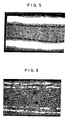
- FIG. 5 is a microanalysis photo of focusing on Ni, in which nickel internal electrodes look as two white bands.
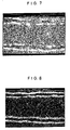
- FIG. 7 is a microanalysis photo focusing on Mn in which Mn rich areas look as four white strips.
- FIG. 9 is a microanalysis photo focusing on P in which P rich areas look as four white strips.
- the capacitor had an effective life of 3.4 hours.
- a multilayer chip capacitor was fabricated by the same procedure as in Example 5 except for the additive and the firing and heat treating conditions.
- the dielectric layers each were 16 ⁇ m thick and consisted essentially of grains having a mean particle size of 3.3 ⁇ m with the percent area of the grain boundary phase being 1.7%.
- the internal electrodes each were 2.5 ⁇ m thick. No oxide layer was formed on the periphery of the internal electrodes.
- the grain boundary phase and grains in the dielectric layer had the following composition.
- the capacitor had an effective life of 1.0 hours.
- a multilayer chip capacitor was fabricated by the same procedure as in Example 10 except for the additive and the firing and heat treating conditions.
- the dielectric layers each were 16 ⁇ m thick and consisted essentially of grains having a mean particle size of 3.1 ⁇ m with the percent area of the grain boundary phase being 0.9%.
- the internal electrodes each were 2.5 ⁇ m thick. No oxide layer was formed on the periphery of the internal electrodes.
- the grain boundary phase and grains in the dielectric layer had the following composition.
- the capacitor had an effective life of 1.4 hours.
- a multilayer chip capacitor of the structure shown in FIG. 2 was fabricated by the same procedure as in Example 10 except for the additive and the firing and heat treating conditions.
- the dielectric layers each were 16 ⁇ m thick and consisted essentially of grains having a mean particle size of 3.6 ⁇ m with the percent area of the grain boundary phase being 1.6%.
- the internal electrodes each were 2.5 ⁇ m thick.
- a single oxide layer of 0.15 ⁇ m thick was formed on the periphery of the internal electrodes.
- the grain boundary phase and grains in the dielectric layer had the following composition.
- the oxide layer had the following composition. Si oxide 1.1% of SiO 2 Al oxide 0.4% of Al 2 O 3 Mn oxide 32.4% of MnO Fe oxide 10.7% of Fe 2 O 3 Ni oxide 8.3% of NiO P oxide 2.1% of P 2 O 5 Ba oxide 3.9% of BaO Ti oxide 40.1% of TiO 2 Ca oxide 0.8% of CaO Zr oxide 0.2% of ZrO 2
- the capacitor had an effective life of 2.1 hours.
- a multilayer chip capacitor of the structure shown in FIG. 2 was fabricated by the same procedure as in Example 10 except for the additive and the firing and heat treating conditions.
- the dielectric layers each were 16 ⁇ m thick and consisted essentially of grains having a mean particle size of 3.6 ⁇ m with the percent area of the grain boundary phase being 0.6%.
- the internal electrodes each were 2.5 ⁇ m thick.
- a single oxide layer of 0.11 ⁇ m thick was formed on the periphery of the internal electrodes.
- the grain boundary phase and grains in the dielectric layer had the following composition.
- the oxide layer had the following composition. Si oxide 0.9% of SiO 2 Al oxide 0.2% of Al 2 O 3 Mn oxide 38.3% of MnO Fe oxide 11.3% of Fe 2 O 3 Ni oxide 9.8% of NiO P oxide 2.2% of P 2 O 5 Ba oxide 7.6% of BaO Ti oxide 29.2% of TiO 2 Ca oxide 0.3% of CaO Zr oxide 0.2% of ZrO 2
- the capacitor had an effective life of 4.1 hours.
- a multilayer chip capacitor was fabricated by the same procedure as in Example 5 except that P 2 O 5 was not added and the firing and heat treating conditions were changed a little.
- the dielectric layers each were 16 ⁇ m thick and consisted essentially of grains having a mean particle size of 3.0 ⁇ m with the percent area of the grain boundary phase being 2.6%.
- the internal electrodes each were 2.5 ⁇ m thick. No oxide layer was formed on the periphery of the internal electrodes.
- the grain boundary phase and grains in the dielectric layer had the following composition.
- the capacitor had an effective life of 0.34 hours.
- Dielectric layer forming pastes were prepared by the same procedure as in Example 5 except that the P 2 O 5 was replaced by the following compounds. These compounds were added alone.
Landscapes
- Engineering & Computer Science (AREA)
- Power Engineering (AREA)
- Manufacturing & Machinery (AREA)
- Microelectronics & Electronic Packaging (AREA)
- Ceramic Engineering (AREA)
- Chemical & Material Sciences (AREA)
- Inorganic Chemistry (AREA)
- Inorganic Insulating Materials (AREA)
- Compositions Of Oxide Ceramics (AREA)
- Ceramic Capacitors (AREA)
Claims (14)
- Condensateur céramique à puce multicouche (1) constitué d'électrodes internes (21, 25) en nickel ou alliage de nickel, et de couches diélectriques (3) superposées en alternance avec les électrodes internes (21, 25),
dans lequel les couches diélectriques (3) consistent essentiellement en grains et en une phase de limite de grain, le pourcentage en surface de la phase de limite de grain pouvant atteindre 2% de la surface d'une coupe de la couche diélectrique (3),
le dit condensateur (1) étant préparé par superposition en alternance d'une matière diélectrique et d'une matière de formation d'électrode interne en nickel ou alliage de nickel, et cuisson de l'empilage,
la dite matière diélectrique est basée sur un oxyde diélectrique de la formule : - Condensateur (1) selon la revendication 1, dans lequel la dite matière diélectrique contient en outre au moins un composant choisi parmi un oxyde de lithium et un composé de lithium qui peut être converti en un oxyde de lithium par cuisson.
- Condensateur (1) selon la revendication 1 ou 2, dans lequel la dite matière diélectrique contient en outre au moins un composant choisi parmi l'oxyde de silicium et l'oxyde de manganèse.
- Condensateur (1) selon la revendication 3, dans lequel la teneur en oxyde de silicium est de 0,05 à 0,25% en poids et la teneur en oxyde de manganèse est de 0,01 à 0,50% en poids sur la base du poids de la matière diélectrique.
- Condensateur (1) selon une des revendications 1 à 4, dans lequel la phase de limite de grain est une phase d'oxyde contenant au moins un élément choisi dans le groupe composé de Al2O3, SiO2 et oxyde phosphoreux.
- Condensateur (1) selon la revendication 5, dans lequel la phase de limite de grain contient au moins 15% en poids de Al2O3 et au moins 15% en poids de SiO2 sur la base du poids de la phase de limite de grain.
- Condensateur (1) selon une quelconque des revendications 1 à 6, dans lequel une couche d'oxyde (4) ayant une composition différente de la dite couche diélectrique (3) est formée sur la périphérie de chaque dite électrode interne (21, 25).
- Condensateur (1) selon la revendication 7, dans lequel la dite couche d'oxyde (4) contient de 1 à 99% en poids, calculé comme MnO, d'oxyde de manganèse.
- Condensateur (1) selon la revendication 7 ou 8, dans lequel la dite couche d'oxyde (4) contient de 0,1 à 99% en poids, calculé comme P2O5, d'oxyde de phosphore.
- Condensateur (1) selon une quelconque des revendications 7 à 9, dans lequel la dite couche d'oxyde (4) contient de 0,1 à 99% en poids, calculé comme Fe2O3, d'oxyde de fer.
- Condensateur (1) selon une quelconque des revendications 7 à 10, dans lequel la dite couche d'oxyde (4) a une épaisseur de 0,01 à 1 µm.
- Condensateur (1) selon une quelconque des revendications 7 à 11, dans lequel la dite couche d'oxyde (4) comprend une première couche contenant de 0,1 à 99% en poids, calculé comme P2O5, d'oxyde de phosphore et une deuxième couche contenant de 1 à 99% en poids, calculé comme MnO, d'oxyde de manganèse.
- Condensateur (1) selon la revendication 12, dans lequel la dite première couche a une épaisseur de 0,005 à 0,995 µm et la dite deuxième couche a une épaisseur de 0,995 à 0,005 µm.
- Procédé de fabrication du condensateur (1) selon une quelconque des revendications 1 à 13, comprenant les étapes de cuisson de l'empilage sous une pression partielle d'oxygène pouvant atteindre 1,01 x 10⁻³Pa (10-8atm) suivie de son traitement thermique à une température de 900 à 1200°C sous une pression partielle d'oxygène d'au moins 1,01 x 10⁻³Pa (10-8atm) afin de réoxyder les couches diélectriques (3) pour former une couche d'oxyde (4) ayant une composition différente de celle des couches diélectriques (3) très près des électrodes internes (21, 25), et de réoxydation des couches diélectriques (3) de sorte que les couches diélectriques (3) consistent essentiellement en grains et en une phase de limite de grain, le pourcentage en surface de la phase de limite de grain pouvant atteindre 2% de la surface d'une coupe des couches diélectriques (3).
Applications Claiming Priority (10)
| Application Number | Priority Date | Filing Date | Title |
|---|---|---|---|
| JP271224/89 | 1989-10-18 | ||
| JP27122689A JP3207847B2 (ja) | 1989-10-18 | 1989-10-18 | 積層型セラミックチップコンデンサ |
| JP271225/89 | 1989-10-18 | ||
| JP27122689 | 1989-10-18 | ||
| JP27122489A JP3207846B2 (ja) | 1989-10-18 | 1989-10-18 | 積層型セラミックチップコンデンサおよびその製造方法 |
| JP271226/89 | 1989-10-18 | ||
| JP1271225A JPH03133115A (ja) | 1989-10-18 | 1989-10-18 | 積層型セラミックチップコンデンサおよびその製造方法 |
| JP27122489 | 1989-10-18 | ||
| JP27122589 | 1989-10-18 | ||
| EP90119856A EP0423738B1 (fr) | 1989-10-18 | 1990-10-16 | Condensateur céramique multicouche sous forme de pastille et son procédé de fabrication |
Related Parent Applications (1)
| Application Number | Title | Priority Date | Filing Date |
|---|---|---|---|
| EP90119856.4 Division | 1990-10-16 |
Publications (3)
| Publication Number | Publication Date |
|---|---|
| EP0623940A2 EP0623940A2 (fr) | 1994-11-09 |
| EP0623940A3 EP0623940A3 (fr) | 1996-12-11 |
| EP0623940B1 true EP0623940B1 (fr) | 2003-01-08 |
Family
ID=27335899
Family Applications (2)
| Application Number | Title | Priority Date | Filing Date |
|---|---|---|---|
| EP94112039A Expired - Lifetime EP0623940B1 (fr) | 1989-10-18 | 1990-10-16 | Condensateur céramique multicouche sous forme de puce et son procédé de fabrication |
| EP90119856A Expired - Lifetime EP0423738B1 (fr) | 1989-10-18 | 1990-10-16 | Condensateur céramique multicouche sous forme de pastille et son procédé de fabrication |
Family Applications After (1)
| Application Number | Title | Priority Date | Filing Date |
|---|---|---|---|
| EP90119856A Expired - Lifetime EP0423738B1 (fr) | 1989-10-18 | 1990-10-16 | Condensateur céramique multicouche sous forme de pastille et son procédé de fabrication |
Country Status (3)
| Country | Link |
|---|---|
| US (1) | US5097391A (fr) |
| EP (2) | EP0623940B1 (fr) |
| DE (2) | DE69027394T2 (fr) |
Families Citing this family (35)
| Publication number | Priority date | Publication date | Assignee | Title |
|---|---|---|---|---|
| JPH05274639A (ja) * | 1992-01-28 | 1993-10-22 | Hitachi Metals Ltd | 非磁性基板材および浮上式磁気ヘッド |
| US5335139A (en) * | 1992-07-13 | 1994-08-02 | Tdk Corporation | Multilayer ceramic chip capacitor |
| US5389428A (en) * | 1992-12-08 | 1995-02-14 | At&T Corp. | Sintered ceramic components and method for making same |
| DE69532235T2 (de) * | 1994-10-19 | 2004-09-16 | Tdk Corp. | Keramischer mehrschicht-chipkondensator |
| US6023408A (en) * | 1996-04-09 | 2000-02-08 | The Board Of Trustees Of The University Of Arkansas | Floating plate capacitor with extremely wide band low impedance |
| JPH104027A (ja) * | 1996-06-14 | 1998-01-06 | Murata Mfg Co Ltd | 積層型電子部品 |
| US6442813B1 (en) | 1996-07-25 | 2002-09-03 | Murata Manufacturing Co., Ltd. | Method of producing a monolithic ceramic capacitor |
| JPH113834A (ja) * | 1996-07-25 | 1999-01-06 | Murata Mfg Co Ltd | 積層セラミックコンデンサおよびその製造方法 |
| JP3567759B2 (ja) | 1998-09-28 | 2004-09-22 | 株式会社村田製作所 | 誘電体セラミック組成物および積層セラミックコンデンサ |
| US6185087B1 (en) | 1999-04-08 | 2001-02-06 | Kemet Electronics Corp. | Multilayer ceramic chip capacitor with high reliability compatible with nickel electrodes |
| JP3596743B2 (ja) * | 1999-08-19 | 2004-12-02 | 株式会社村田製作所 | 積層セラミック電子部品の製造方法及び積層セラミック電子部品 |
| US6368514B1 (en) | 1999-09-01 | 2002-04-09 | Luminous Intent, Inc. | Method and apparatus for batch processed capacitors using masking techniques |
| JP2001114569A (ja) * | 1999-10-20 | 2001-04-24 | Murata Mfg Co Ltd | セラミックスラリー組成物、セラミックグリーンシート及び積層セラミック電子部品の製造方法 |
| EP1378922B1 (fr) * | 2001-04-12 | 2009-07-15 | TDK Corporation | Procede de production de composant electronique en ceramique multicouche |
| DE60335427D1 (de) * | 2002-01-15 | 2011-02-03 | Tdk Corp | Dielektrische keramische Zusammensetzung und elektronische Vorrichtung |
| JP3744439B2 (ja) * | 2002-02-27 | 2006-02-08 | 株式会社村田製作所 | 導電性ペーストおよび積層セラミック電子部品 |
| JP3882718B2 (ja) * | 2002-08-29 | 2007-02-21 | 株式会社村田製作所 | 薄膜積層電子部品の製造方法 |
| US6869895B1 (en) * | 2003-09-30 | 2005-03-22 | International Business Machines Corporation | Method for adjusting capacitance of an on-chip capacitor |
| US7224570B2 (en) * | 2004-06-28 | 2007-05-29 | Kyocera Corporation | Process for preparing multilayer ceramic capacitor and the multilayer ceramic capacitor |
| JP4295179B2 (ja) * | 2004-08-31 | 2009-07-15 | Tdk株式会社 | 電子部品およびその製造方法 |
| US7528088B2 (en) * | 2005-04-01 | 2009-05-05 | Tdk Corporation | Electronic device |
| US7230817B2 (en) * | 2005-04-15 | 2007-06-12 | Ferro Corporation | Y5V dielectric composition |
| KR100925656B1 (ko) * | 2005-05-10 | 2009-11-09 | 가부시키가이샤 무라타 세이사쿠쇼 | 박막 커패시터의 제조방법 |
| KR100773534B1 (ko) * | 2005-07-15 | 2007-11-05 | 삼성전기주식회사 | 혼합 분산제, 이를 이용한 페이스트 조성물 및 분산방법 |
| JP2007035848A (ja) * | 2005-07-26 | 2007-02-08 | Taiyo Yuden Co Ltd | 積層セラミックコンデンサ及びその製造方法 |
| JPWO2007026562A1 (ja) * | 2005-08-29 | 2009-03-05 | 京セラ株式会社 | 金属膜およびその製法、並びに、積層型電子部品の製法および積層型電子部品 |
| US7685687B2 (en) * | 2007-01-22 | 2010-03-30 | E. I. Du Pont De Nemours And Company | Methods of making high capacitance density ceramic capacitors |
| US8875363B2 (en) * | 2008-09-25 | 2014-11-04 | Cda Processing Limited Liability Company | Thin film capacitors on metal foils and methods of manufacturing same |
| KR101462761B1 (ko) * | 2013-02-13 | 2014-11-20 | 삼성전기주식회사 | 다층 세라믹 소자 및 그 제조 방법 |
| JP2017228731A (ja) * | 2016-06-24 | 2017-12-28 | 京セラ株式会社 | 積層型電子部品 |
| KR102163417B1 (ko) * | 2018-08-09 | 2020-10-08 | 삼성전기주식회사 | 적층 세라믹 커패시터 |
| KR102351180B1 (ko) | 2019-02-13 | 2022-01-17 | 삼성전기주식회사 | 적층 세라믹 커패시터 |
| US12315681B2 (en) * | 2021-09-14 | 2025-05-27 | Samsung Electro-Mechanics Co., Ltd. | Ceramic electronic component having a dielectric with secondary phases, method of manufacturing ceramic electronic component, and method of producing dielectric powder |
| JP2023109441A (ja) * | 2022-01-27 | 2023-08-08 | 株式会社村田製作所 | 3端子型積層セラミックコンデンサ |
| KR20230117793A (ko) | 2022-02-03 | 2023-08-10 | 삼성전기주식회사 | 적층형 전자 부품 |
Family Cites Families (11)
| Publication number | Priority date | Publication date | Assignee | Title |
|---|---|---|---|---|
| US4097911A (en) * | 1975-10-06 | 1978-06-27 | Erie Technological Products, Inc. | Base metal electrode capacitor and method of making the same |
| JPS5324600A (en) * | 1976-08-19 | 1978-03-07 | Murata Manufacturing Co | Nonnreducing dielectric ceramic composition |
| US4241378A (en) * | 1978-06-12 | 1980-12-23 | Erie Technological Products, Inc. | Base metal electrode capacitor and method of making the same |
| DE3138177A1 (de) * | 1981-09-25 | 1983-04-14 | Philips Patentverwaltung Gmbh, 2000 Hamburg | "verfahren zur herstellung eines dielektrikums" |
| JPS58143512A (ja) * | 1982-02-19 | 1983-08-26 | ニチコン株式会社 | 積層セラミツクコンデンサ |
| JPS5927518A (ja) * | 1982-08-05 | 1984-02-14 | ニチコン株式会社 | 積層セラミツクコンデンサ |
| US4604676A (en) * | 1984-10-02 | 1986-08-05 | Murata Manufacturing Co., Ltd. | Ceramic capacitor |
| US4612600A (en) * | 1984-10-29 | 1986-09-16 | Tam Ceramics Inc. | Low fire ceramic compositions |
| JPS61147404A (ja) * | 1984-12-18 | 1986-07-05 | 太陽誘電株式会社 | 誘電体磁器組成物 |
| DE3764201D1 (de) * | 1986-06-19 | 1990-09-13 | Akzo Nv | Verfahren zum beschichten eines synthetischen substrats mit einem grundiermittel und einem deckanstrich und die grundiermittel fuer dieses verfahren. |
| US4988650A (en) * | 1989-06-23 | 1991-01-29 | Murata Manufacturing Co., Ltd. | Auxiliary agent for sintering ceramic material |
-
1990
- 1990-10-16 DE DE69027394T patent/DE69027394T2/de not_active Expired - Lifetime
- 1990-10-16 EP EP94112039A patent/EP0623940B1/fr not_active Expired - Lifetime
- 1990-10-16 EP EP90119856A patent/EP0423738B1/fr not_active Expired - Lifetime
- 1990-10-16 DE DE69034034T patent/DE69034034T2/de not_active Expired - Lifetime
- 1990-10-18 US US07/599,414 patent/US5097391A/en not_active Expired - Lifetime
Also Published As
| Publication number | Publication date |
|---|---|
| EP0423738A2 (fr) | 1991-04-24 |
| EP0623940A2 (fr) | 1994-11-09 |
| EP0623940A3 (fr) | 1996-12-11 |
| US5097391A (en) | 1992-03-17 |
| DE69034034D1 (de) | 2003-02-13 |
| DE69034034T2 (de) | 2003-10-16 |
| DE69027394D1 (de) | 1996-07-18 |
| EP0423738B1 (fr) | 1996-06-12 |
| DE69027394T2 (de) | 1997-02-06 |
| EP0423738A3 (en) | 1992-12-02 |
Similar Documents
| Publication | Publication Date | Title |
|---|---|---|
| EP0623940B1 (fr) | Condensateur céramique multicouche sous forme de puce et son procédé de fabrication | |
| US5319517A (en) | Multilayer ceramic chip capacitor | |
| CN114334447B (zh) | 层叠陶瓷电容器 | |
| JP4991564B2 (ja) | 積層セラミックコンデンサ | |
| KR102351180B1 (ko) | 적층 세라믹 커패시터 | |
| DE60014225T2 (de) | Keramischer Vielschichtkondensator mit hoher Zuverlässigkeit, kompatibel mit Nickelelektroden | |
| KR100414331B1 (ko) | 비환원성 유전체 세라믹 및 이것을 사용한 모놀리식 세라믹 커패시터 | |
| EP0534378B1 (fr) | Composition céramique diélectrique non-réductible | |
| KR102430851B1 (ko) | 유전체 자기 조성물 및 세라믹 전자 부품 | |
| US7638451B2 (en) | Dielectric ceramic, method of producing the same, and monolithic ceramic capacitor | |
| EP1095917A1 (fr) | Composition ceramique dielectrique, son emploi dans un condensateur et son procede de fabrication | |
| JP4480367B2 (ja) | 誘電体磁器およびその製法、並びに積層型電子部品およびその製法 | |
| JPH11273985A (ja) | 誘電体セラミックおよびその製造方法、ならびに、積層セラミック電子部品およびその製造方法 | |
| US10618846B2 (en) | Dielectric porcelain composition, multilayer ceramic capacitor, and method for producing multilayer ceramic capacitor | |
| CN1317457A (zh) | 非还原性介电陶瓷,其制造方法和用该陶瓷的单块电容器 | |
| EP1712533A2 (fr) | Procédé de production d'une composition céramique et procédé de fabrication d'un dispositif électronique | |
| KR20190121143A (ko) | 적층 세라믹 커패시터 | |
| EP0630032B1 (fr) | Composition céramique diélectrique non-réductible | |
| EP1786005B1 (fr) | Composition céramique diélectrique, composant électronique, et condensateur céramique multicouche | |
| KR100374471B1 (ko) | 유전체 세라믹 재료 및 모놀리식 세라믹 전자 부품 | |
| KR20220108721A (ko) | 세라믹 전자 부품 및 그 제조 방법 | |
| JP3207847B2 (ja) | 積層型セラミックチップコンデンサ | |
| JP3419713B2 (ja) | 積層型セラミックチップコンデンサの製造方法 | |
| JP4511323B2 (ja) | 積層セラミックコンデンサおよびその製法 | |
| US6743518B2 (en) | Ceramic capacitor and method for the manufacture thereof |
Legal Events
| Date | Code | Title | Description |
|---|---|---|---|
| PUAI | Public reference made under article 153(3) epc to a published international application that has entered the european phase |
Free format text: ORIGINAL CODE: 0009012 |
|
| AC | Divisional application: reference to earlier application |
Ref document number: 423738 Country of ref document: EP |
|
| AK | Designated contracting states |
Kind code of ref document: A2 Designated state(s): DE FR GB NL |
|
| PUAL | Search report despatched |
Free format text: ORIGINAL CODE: 0009013 |
|
| AK | Designated contracting states |
Kind code of ref document: A3 Designated state(s): DE FR GB NL |
|
| 17P | Request for examination filed |
Effective date: 19970115 |
|
| 17Q | First examination report despatched |
Effective date: 19990629 |
|
| GRAG | Despatch of communication of intention to grant |
Free format text: ORIGINAL CODE: EPIDOS AGRA |
|
| GRAG | Despatch of communication of intention to grant |
Free format text: ORIGINAL CODE: EPIDOS AGRA |
|
| GRAH | Despatch of communication of intention to grant a patent |
Free format text: ORIGINAL CODE: EPIDOS IGRA |
|
| GRAH | Despatch of communication of intention to grant a patent |
Free format text: ORIGINAL CODE: EPIDOS IGRA |
|
| GRAA | (expected) grant |
Free format text: ORIGINAL CODE: 0009210 |
|
| AC | Divisional application: reference to earlier application |
Ref document number: 423738 Country of ref document: EP |
|
| AK | Designated contracting states |
Kind code of ref document: B1 Designated state(s): DE FR GB NL |
|
| REG | Reference to a national code |
Ref country code: GB Ref legal event code: FG4D |
|
| REF | Corresponds to: |
Ref document number: 69034034 Country of ref document: DE Date of ref document: 20030213 Kind code of ref document: P |
|
| ET | Fr: translation filed | ||
| PLBE | No opposition filed within time limit |
Free format text: ORIGINAL CODE: 0009261 |
|
| STAA | Information on the status of an ep patent application or granted ep patent |
Free format text: STATUS: NO OPPOSITION FILED WITHIN TIME LIMIT |
|
| 26N | No opposition filed |
Effective date: 20031009 |
|
| PGFP | Annual fee paid to national office [announced via postgrant information from national office to epo] |
Ref country code: NL Payment date: 20081015 Year of fee payment: 19 |
|
| PGFP | Annual fee paid to national office [announced via postgrant information from national office to epo] |
Ref country code: FR Payment date: 20081014 Year of fee payment: 19 |
|
| PGFP | Annual fee paid to national office [announced via postgrant information from national office to epo] |
Ref country code: GB Payment date: 20081015 Year of fee payment: 19 |
|
| PGFP | Annual fee paid to national office [announced via postgrant information from national office to epo] |
Ref country code: DE Payment date: 20091008 Year of fee payment: 20 |
|
| REG | Reference to a national code |
Ref country code: NL Ref legal event code: V1 Effective date: 20100501 |
|
| REG | Reference to a national code |
Ref country code: FR Ref legal event code: ST Effective date: 20100630 |
|
| PG25 | Lapsed in a contracting state [announced via postgrant information from national office to epo] |
Ref country code: NL Free format text: LAPSE BECAUSE OF NON-PAYMENT OF DUE FEES Effective date: 20100501 Ref country code: FR Free format text: LAPSE BECAUSE OF NON-PAYMENT OF DUE FEES Effective date: 20091102 |
|
| PG25 | Lapsed in a contracting state [announced via postgrant information from national office to epo] |
Ref country code: GB Free format text: LAPSE BECAUSE OF NON-PAYMENT OF DUE FEES Effective date: 20091016 |
|
| PG25 | Lapsed in a contracting state [announced via postgrant information from national office to epo] |
Ref country code: DE Free format text: LAPSE BECAUSE OF EXPIRATION OF PROTECTION Effective date: 20101016 |