EP0594049A1 - Bipolarer Transistor mit isolierter Steuerelektrode und Verfahren zur Herstellung desselben - Google Patents
Bipolarer Transistor mit isolierter Steuerelektrode und Verfahren zur Herstellung desselben Download PDFInfo
- Publication number
- EP0594049A1 EP0594049A1 EP93116565A EP93116565A EP0594049A1 EP 0594049 A1 EP0594049 A1 EP 0594049A1 EP 93116565 A EP93116565 A EP 93116565A EP 93116565 A EP93116565 A EP 93116565A EP 0594049 A1 EP0594049 A1 EP 0594049A1
- Authority
- EP
- European Patent Office
- Prior art keywords
- semiconductor region
- semiconductor
- region
- conductivity type
- type semiconductor
- Prior art date
- Legal status (The legal status is an assumption and is not a legal conclusion. Google has not performed a legal analysis and makes no representation as to the accuracy of the status listed.)
- Granted
Links
- 238000004519 manufacturing process Methods 0.000 title claims description 53
- 239000004065 semiconductor Substances 0.000 claims abstract description 507
- 239000012535 impurity Substances 0.000 claims description 86
- 238000000034 method Methods 0.000 claims description 31
- 239000011159 matrix material Substances 0.000 claims description 2
- 239000000758 substrate Substances 0.000 abstract description 21
- 230000006378 damage Effects 0.000 abstract description 9
- 238000002347 injection Methods 0.000 abstract description 9
- 239000007924 injection Substances 0.000 abstract description 9
- 239000010408 film Substances 0.000 description 14
- 238000004088 simulation Methods 0.000 description 9
- 108091006146 Channels Proteins 0.000 description 7
- XUIMIQQOPSSXEZ-UHFFFAOYSA-N Silicon Chemical compound [Si] XUIMIQQOPSSXEZ-UHFFFAOYSA-N 0.000 description 7
- 238000009413 insulation Methods 0.000 description 7
- 238000000206 photolithography Methods 0.000 description 7
- 230000008569 process Effects 0.000 description 7
- 229910052710 silicon Inorganic materials 0.000 description 7
- 239000010703 silicon Substances 0.000 description 7
- 239000000969 carrier Substances 0.000 description 6
- 229910052782 aluminium Inorganic materials 0.000 description 4
- XAGFODPZIPBFFR-UHFFFAOYSA-N aluminium Chemical compound [Al] XAGFODPZIPBFFR-UHFFFAOYSA-N 0.000 description 4
- 230000015572 biosynthetic process Effects 0.000 description 4
- 230000015556 catabolic process Effects 0.000 description 4
- 238000009792 diffusion process Methods 0.000 description 4
- 229910021420 polycrystalline silicon Inorganic materials 0.000 description 4
- 230000009467 reduction Effects 0.000 description 4
- 230000008859 change Effects 0.000 description 3
- 230000003071 parasitic effect Effects 0.000 description 3
- 229920005591 polysilicon Polymers 0.000 description 3
- 230000004044 response Effects 0.000 description 3
- 102000004129 N-Type Calcium Channels Human genes 0.000 description 2
- 108090000699 N-Type Calcium Channels Proteins 0.000 description 2
- 230000000694 effects Effects 0.000 description 2
- 230000006872 improvement Effects 0.000 description 2
- 229910052751 metal Inorganic materials 0.000 description 2
- 239000002184 metal Substances 0.000 description 2
- 230000005684 electric field Effects 0.000 description 1
- -1 i.e. Substances 0.000 description 1
- 230000004048 modification Effects 0.000 description 1
- 238000012986 modification Methods 0.000 description 1
- 238000002360 preparation method Methods 0.000 description 1
- 239000010409 thin film Substances 0.000 description 1
Images


Classifications
-
- H—ELECTRICITY
- H01—ELECTRIC ELEMENTS
- H01L—SEMICONDUCTOR DEVICES NOT COVERED BY CLASS H10
- H01L29/00—Semiconductor devices specially adapted for rectifying, amplifying, oscillating or switching and having potential barriers; Capacitors or resistors having potential barriers, e.g. a PN-junction depletion layer or carrier concentration layer; Details of semiconductor bodies or of electrodes thereof ; Multistep manufacturing processes therefor
- H01L29/66—Types of semiconductor device ; Multistep manufacturing processes therefor
- H01L29/66007—Multistep manufacturing processes
- H01L29/66075—Multistep manufacturing processes of devices having semiconductor bodies comprising group 14 or group 13/15 materials
- H01L29/66227—Multistep manufacturing processes of devices having semiconductor bodies comprising group 14 or group 13/15 materials the devices being controllable only by the electric current supplied or the electric potential applied, to an electrode which does not carry the current to be rectified, amplified or switched, e.g. three-terminal devices
- H01L29/66234—Bipolar junction transistors [BJT]
- H01L29/66325—Bipolar junction transistors [BJT] controlled by field-effect, e.g. insulated gate bipolar transistors [IGBT]
- H01L29/66333—Vertical insulated gate bipolar transistors
-
- H—ELECTRICITY
- H01—ELECTRIC ELEMENTS
- H01L—SEMICONDUCTOR DEVICES NOT COVERED BY CLASS H10
- H01L29/00—Semiconductor devices specially adapted for rectifying, amplifying, oscillating or switching and having potential barriers; Capacitors or resistors having potential barriers, e.g. a PN-junction depletion layer or carrier concentration layer; Details of semiconductor bodies or of electrodes thereof ; Multistep manufacturing processes therefor
- H01L29/02—Semiconductor bodies ; Multistep manufacturing processes therefor
- H01L29/06—Semiconductor bodies ; Multistep manufacturing processes therefor characterised by their shape; characterised by the shapes, relative sizes, or dispositions of the semiconductor regions ; characterised by the concentration or distribution of impurities within semiconductor regions
- H01L29/08—Semiconductor bodies ; Multistep manufacturing processes therefor characterised by their shape; characterised by the shapes, relative sizes, or dispositions of the semiconductor regions ; characterised by the concentration or distribution of impurities within semiconductor regions with semiconductor regions connected to an electrode carrying current to be rectified, amplified or switched and such electrode being part of a semiconductor device which comprises three or more electrodes
- H01L29/083—Anode or cathode regions of thyristors or gated bipolar-mode devices
- H01L29/0834—Anode regions of thyristors or gated bipolar-mode devices, e.g. supplementary regions surrounding anode regions
-
- H—ELECTRICITY
- H01—ELECTRIC ELEMENTS
- H01L—SEMICONDUCTOR DEVICES NOT COVERED BY CLASS H10
- H01L29/00—Semiconductor devices specially adapted for rectifying, amplifying, oscillating or switching and having potential barriers; Capacitors or resistors having potential barriers, e.g. a PN-junction depletion layer or carrier concentration layer; Details of semiconductor bodies or of electrodes thereof ; Multistep manufacturing processes therefor
- H01L29/66—Types of semiconductor device ; Multistep manufacturing processes therefor
- H01L29/66007—Multistep manufacturing processes
- H01L29/66075—Multistep manufacturing processes of devices having semiconductor bodies comprising group 14 or group 13/15 materials
- H01L29/66227—Multistep manufacturing processes of devices having semiconductor bodies comprising group 14 or group 13/15 materials the devices being controllable only by the electric current supplied or the electric potential applied, to an electrode which does not carry the current to be rectified, amplified or switched, e.g. three-terminal devices
- H01L29/66234—Bipolar junction transistors [BJT]
- H01L29/66325—Bipolar junction transistors [BJT] controlled by field-effect, e.g. insulated gate bipolar transistors [IGBT]
- H01L29/66333—Vertical insulated gate bipolar transistors
- H01L29/66348—Vertical insulated gate bipolar transistors with a recessed gate
-
- H—ELECTRICITY
- H01—ELECTRIC ELEMENTS
- H01L—SEMICONDUCTOR DEVICES NOT COVERED BY CLASS H10
- H01L29/00—Semiconductor devices specially adapted for rectifying, amplifying, oscillating or switching and having potential barriers; Capacitors or resistors having potential barriers, e.g. a PN-junction depletion layer or carrier concentration layer; Details of semiconductor bodies or of electrodes thereof ; Multistep manufacturing processes therefor
- H01L29/66—Types of semiconductor device ; Multistep manufacturing processes therefor
- H01L29/68—Types of semiconductor device ; Multistep manufacturing processes therefor controllable by only the electric current supplied, or only the electric potential applied, to an electrode which does not carry the current to be rectified, amplified or switched
- H01L29/70—Bipolar devices
- H01L29/72—Transistor-type devices, i.e. able to continuously respond to applied control signals
- H01L29/739—Transistor-type devices, i.e. able to continuously respond to applied control signals controlled by field-effect, e.g. bipolar static induction transistors [BSIT]
- H01L29/7393—Insulated gate bipolar mode transistors, i.e. IGBT; IGT; COMFET
- H01L29/7395—Vertical transistors, e.g. vertical IGBT
- H01L29/7396—Vertical transistors, e.g. vertical IGBT with a non planar surface, e.g. with a non planar gate or with a trench or recess or pillar in the surface of the emitter, base or collector region for improving current density or short circuiting the emitter and base regions
- H01L29/7397—Vertical transistors, e.g. vertical IGBT with a non planar surface, e.g. with a non planar gate or with a trench or recess or pillar in the surface of the emitter, base or collector region for improving current density or short circuiting the emitter and base regions and a gate structure lying on a slanted or vertical surface or formed in a groove, e.g. trench gate IGBT
-
- H—ELECTRICITY
- H01—ELECTRIC ELEMENTS
- H01L—SEMICONDUCTOR DEVICES NOT COVERED BY CLASS H10
- H01L21/00—Processes or apparatus adapted for the manufacture or treatment of semiconductor or solid state devices or of parts thereof
- H01L21/02—Manufacture or treatment of semiconductor devices or of parts thereof
- H01L21/04—Manufacture or treatment of semiconductor devices or of parts thereof the devices having potential barriers, e.g. a PN junction, depletion layer or carrier concentration layer
- H01L21/18—Manufacture or treatment of semiconductor devices or of parts thereof the devices having potential barriers, e.g. a PN junction, depletion layer or carrier concentration layer the devices having semiconductor bodies comprising elements of Group IV of the Periodic Table or AIIIBV compounds with or without impurities, e.g. doping materials
- H01L21/185—Joining of semiconductor bodies for junction formation
- H01L21/187—Joining of semiconductor bodies for junction formation by direct bonding
Definitions
- the present invention relates to an insulated gate semiconductor device such as an insulated gate bipolar transistor (hereinafter abbreviated as "IGBT") and a method of manufacturing the same.
- IGBT insulated gate bipolar transistor
- An insulated gate bipolar transistor is a semiconductor device which has a structure in which p-type semiconductor regions and n-type semiconductor regions are joined so that at least four semiconductor regions of alternate conductivity type are disposed in series.
- the two outer semiconductor regions at least, are electrically connected to a positive and a negative main electrodes, respectively.
- a gate electrode for applying an electric field is connected to one of the two inner semiconductor regions.
- a current which flows between the two main electrodes changes in accordance with a voltage which is applied to the gate electrode.
- An IGBT, an EST (Emitter Switched Thyristor), a MCT (MOS Controlled Thyristor) and the like fall within this category of semiconductor device.
- Fig. 20 is a cross sectional view showing the structure of a conventional N-channel type IGBT.
- an IGBT is comprised of a number of IGBT elements (hereinafter "unit cells") which are connected parallel to each other.
- Fig. 20 shows a cross section of one unit cell.
- an n-type semiconductor layer 11 is formed on a p-type semiconductor layer 1 which includes a p-type semiconductor substrate, whereby a semiconductor substrate body 12 is formed.
- a p-type base region 4 is formed by selective diffusion of p-type impurities.
- an n-type emitter region 5 is formed by selective diffusion of n-type impurities.
- a gate insulation film 7 is disposed on top surface of the p-type base region 4 between the top surface of the n-type semiconductor layer 11 and the top major surface of the n-type emitter region 5.
- a gate electrode 8 which is made of polycrystalline silicon (hereinafter simply as "polysilicon") is formed on the gate insulation film 7, a gate electrode 8 which is made of polycrystalline silicon (hereinafter simply as "polysilicon”) is formed.
- An emitter electrode 9 made of aluminum is disposed in electrical connection to both the p-type base region 4 and the n-type emitter region 5.
- the gate electrode 8 and the emitter electrode 9 are insulated from each other.
- the gate electrodes 8 of the respective unit cells are electrically connected with each other and the emitter electrodes 9 of the respective unit cells are also electrically connected with each other.
- a collector electrode 10 which is made of metal such as aluminum is electrically connected to the bottom major surface of the p-type semiconductor layer 1.
- the collector electrodes 10 of the respective unit cells are contiguous with each other.
- the n-type semiconductor layer 11 includes a buffer layer 2 which is heavily doped n-type where it abuts the p-type semiconductor layer 1.
- the n-type semiconductor layer 3 excluding the buffer layer 2 has an impurity concentration of about 1014 cm ⁇ 3 (In general, the withstand voltage becomes higher in proportion to decrease of the impurity concentration. The following description will be made for the IGBT having a withstand voltage class of 600V.)
- the concentration of n-type impurities is about 1017 cm ⁇ 3.
- a predetermined collector voltage V CE is applied between the emitter electrode 9 and the collector electrode 10. If in addition to this, a gate voltage V GE exceeding a threshold value which the device inherently has is applied between the emitter electrode 9 and the gate electrode 8, the p-type base region 4 is inverted into the n-type at a channel region 6 which is located in the vicinity of the gate electrode 8, thereby creating an n-type channel at the channel region 6. Through this channel, carriers, in this case electrons, are introduced from the emitter electrode 9 into the n-type semiconductor layer 3.
- a forward bias is applied between the p-type semiconductor layer 1 and the n-type semiconductor layer 11, causing injection of carriers, i.e., holes in this case, from the p-type semiconductor layer 1.
- the resistance of the p-type semiconductor layer 1 drops largely so that a collector current I C flowing from the collector electrode 10 to the emitter electrode 9 drastically increases.
- the device turns conductive (i.e., turns on).
- a resistance against the collector current I C at such an occasion is called an ON-resistance.
- the ON-resistance is in most cases expressed as the collector voltage V CE when the collector current I C is equal to a normal rated current value (i.e., saturation collector voltage V CE (sat)).
- the normal rated current of the conventional IGBT is typically around 50 to 150 A/cm2.
- the resistance of the n-type semiconductor layer 11 is reduced by means of injection of holes from the p-type semiconductor layer 1.
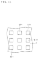
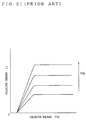
- Fig. 21 is a graph showing output characteristics of the device in response to various gate voltages V GE .
- the collector voltage V CE is increased while the gate voltage V GE of a certain value is applied, the flow rate of electrons flowing in the channel is suppressed by a certain amount which corresponds to the gate voltage V GE .
- the collector current I C flowing in the device saturates at a constant value which corresponds to the gate voltage V GE , that is, at a saturation collector current I C (sat) (horizontal straight portions of the curves in Fig. 21).
- the buffer layer 2 controls injection of holes from the p-type semiconductor layer 1.
- holes from the p-type semiconductor layer 1 easily combine with electrons which exist in the buffer layer 2.
- provision of the buffer layer 2 lowers the saturation collector current I C (sat) while enhances the ON-resistance.
- the saturation collector current I C (sat) and the ON-resistance can be adjusted.
- the collector voltage V CE is increased under OFF-state of the device by means of a reduction in the gate voltage V GE to zero or other suitable method, the collector current I C would not be started until the collector voltage V CE reaches a certain value. However, once the collector voltage V CE has grown beyond the certain value, the collector current I C will start flowing and become increasingly large.
- the collector voltage V CE at this stage is referred to as "breakdown voltage.”
- the collector voltage V CE which can be applied to the IGBT is less than the breakdown voltage.
- the IGBT includes a parasitic thyristor which is formed by the n-type emitter region 5, the n-type semiconductor layer 11 and the p-type semiconductor layer 1.
- the parasitic thyristor turns on if the collector current I C exceeds a certain value (i.e., latch up current) (Ts is known as "latching up of the IGBT").
- Ts latch up current
- the buffer layer 2 is formed having a thickness which would allow injection of holes from the p-type semiconductor layer 1 in a great number in order to reduce the ON-resistance, the value of the saturation collector current I C (sat) which is developed in response to application of a certain gate voltage V GE would increase. If the saturation collector current I C (sat) is large, the collector current I C tends to exceed the latch up current during the operations of the IGBT. The result of this is an increased possibility of destruction of the IGBT due to latch up.
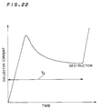
- Fig. 22 is a graph showing the waveform of the collector current I C with a change in time after the short circuiting. Immediately after the short circuiting, the collector current I C exhibits an abrupt increase, amounting to a maximum value which is about 5 to 20 times as large as the normal rated current value (50 to 150 A/cm2). It is when the collector current I C is at this maximum level that the IGBT is most likely to be destroyed due to latch up.
- the collector current I C reached the maximum level, even if latch up has not occurred, a continued unusually large collector current I C far beyond a normal level under normal environment is still observed. Due to this, the IGBT will be destroyed after a certain time Tv.
- the time Tv during which the IGBT remains undestroyed though short circuiting, must be longer than 10 to 20 ⁇ sec for practical reasons. In the art, it is a general knowledge that the lower the collector current I C is during short circuiting of the device, the longer the time Tv is.
- the collector current I C during short circuiting is defined at a value of the saturation collector current I C (sat).
- the value of the saturation collector current I C (sat) in response to application of a certain gate voltage V GE would increase. If the saturation collector current I C (sat) is large, the collector current I C under short circuiting becomes large, and therefore, the time Tv becomes short.
- the conventional IGBT has a drawback that a low ON-resistance easily causes destruction of the IGBT due to latch up and subsequent short circuiting (short-circuit destruction).
- the present invention is directed to an insulated gate semiconductor device.
- the device comprises: a first semiconductor region of a first conductivity type; a second semiconductor region of a second conductivity type formed on the first semiconductor region; a third semiconductor region of the first conductivity type selectively formed in a top portion of the second semiconductor region; a fourth semiconductor region of the second conductivity type selectively formed in a top portion of the third semiconductor region; a fifth semiconductor region of the second conductivity type selectively formed in a bottom portion of the second semiconductor region and having a gap positioned at a desired position relative to the third and the fourth semiconductor regions and having a higher concentration of impurities of the second type than the second semiconductor region; an insulating layer formed on the third and the fourth semiconductor regions; a first main electrode electrically connected to the first semiconductor region; a second main electrode electrically connected to the fourth semiconductor region; and a control electrode formed on the insulating layer.
- the insulated gate semiconductor device In the insulated gate semiconductor device according to the present invention, injection of carriers from the first semiconductor region to the second semiconductor region is attained by carriers which selectively flow in a region where the fifth semiconductor region is not present.
- a current which flows between the first and the second main electrodes is small, under a predominant influence of a fact that the carrier concentration at such a region is higher than where the device does not comprise the fifth semiconductor region, flow of the current is facilitated. In other words, the ON-resistance of the device becomes lower than that where the fifth semiconductor region is not provided.
- the second semiconductor region comprises: a first semiconductor portion formed on the top major surface of the first semiconductor region and having a concentration of impurities of the second conductivity type which is lower than that of the fifth semiconductor region; and a second semiconductor portion formed on a top major surface of the first semiconductor portion and having a concentration of impurities of the second conductivity type which is lower than that of the first semiconductor portion.
- the first portion of the second semiconductor region prevents a depletion region which grows from the third semiconductor region from reaching the first semiconductor region. Hence, even if the second semiconductor region is thin, there is no possibility that punch through will be caused.
- the concentration of impurities of the second semiconductor portion is substantially equal to or less than 5 ⁇ 1014 cm ⁇ 3
- the concentration of impurities of the first semiconductor portion is selected from the range substantially defined from 5 ⁇ 1014 cm ⁇ 3 to 1017 cm ⁇ 3
- the concentration of impurities of the fifth semiconductor region is selected from the range substantially defined from 1018 cm ⁇ 3 to 1021 cm ⁇ 3.
- the impurity concentrations of the second conductivity type in the second, the fifth and the sixth semiconductor regions are optimized. Hence, a reduction in the ON-resistance and an improvement in the breakdown voltage are better achieved in the device.
- the present invention is also directed to a method of manufacturing an insulated gate semiconductor device.
- the method comprises the steps of: (a) obtaining a first semiconductor region of a first conductivity type; (b) obtaining, on a top major surface of the first semiconductor region, a structure in which a second semiconductor region of a second conductivity type is formed on the top major surface of the first semiconductor region and a third semiconductor region of a second conductivity type is selectively formed in a bottom portion of the second semiconductor region, wherein an impurity concentration of the third semiconductor region is higher than that of the second semiconductor region; (c) selectively forming a fourth semiconductor region of the first conductivity type in a top portion of the second semiconductor region, the fourth semiconductor region comprising first and second portions laterally separated from each other; (d) selectively forming a fifth semiconductor region of the second conductivity type in the fourth semiconductor region, the fifth semiconductor region comprising first and second portions selectively formed in the first and second portions of the fourth semiconductor region; (e) forming a first main electrode layer on a bottom major surface of the first semiconductor region; (f) forming a second main electrode layer on a
- the device according to the present invention may be manufactured in through the steps of: (a) obtaining a first semiconductor region of a first conductivity type; (b) obtaining, on a bottom major surface of the first semiconductor region, a structure in which a second semiconductor region of a second conductivity type is formed and a third semiconductor region of a first conductivity type is selectively formed in a top portion of the structure, wherein an impurity concentration of the third semiconductor region is higher than that of the first semiconductor region; (c) selectively forming a fourth semiconductor region of the second conductivity type in a top portion of the first semiconductor region; (d) selectively forming a fifth semiconductor region of the first conductivity type in the fourth semiconductor region; (e) forming a first main electrode layer on a bottom surface of the second semiconductor region; (f) forming a second main electrode layer on a top major surface of the fifth semiconductor region; (g) forming an insulating layer which is in contact with the fourth semiconductor region; and (h) forming a control electrode layer on the insulating layer
- an object of the present invention to obtain an insulated gate semiconductor device which has a low ON-resistance and an enhanced durability against destruction.
- Another object of the present invention is to obtain a method of manufacturing such an insulated gate semiconductor device.
- Fig. 1 is a cross sectional view showing the structure of an insulated gate semiconductor device according to a first preferred embodiment of the present invention.
- the illustrated device is an IGBT of a withstand voltage class of 600V.
- the IGBT of the first preferred embodiment has a structure in which a number of unit cells are connected in parallel with each other.
- Fig. 1 shows a cross section of one unit cell.
- elements or parts corresponding to the same or equivalent elements are denoted by the same reference numerals.
- an n-type semiconductor layer 11 is formed on a p-type semiconductor layer 1 which includes a p-type semiconductor substrate, whereby a semiconductor substrate body 12 is formed.
- a p-type base region 4 is formed by selective diffusion of p-type impurities.
- the base region 4 comprises first and second portions 4a and 4b in the section illustrated in Fig. 1, portions 4a and 4b being separated from each other.
- an n-type emitter region 5 is formed by selective diffusion of n-type impurities.
- a region outside the p-type base region 4 and the n-type emitter region 5 are isolated from each other by the p-type base region 4.
- the emitter region 5 comprises first and second portions 5a and 5b in the section illustrated in Fig. 1.
- a gate insulation film 7 i.e., insulating layer
- a gate electrode 8 which is made of polysilicon (i.e., control electrode layer), for example, is formed facing the top surface of p-type base region 4.
- An emitter electrode 9 made of aluminum (second main electrode layer) is disposed in electrical connection to both the p-type base region 4 and the n-type emitter region 5. The gate electrode 8 and the emitter electrode 9 are insulated from each other.
- the gate electrodes 8 of the respective unit cells are electrically connected with each other and the emitter electrodes 9 of the respective unit cells are also electrically connected with each other.
- a collector electrode 10 which is made of metal such as aluminum (first main electrode layer) is electrically connected to the bottom major surface of the p-type semiconductor layer 1.
- the collector electrodes 10 of the respective unit cells are contiguous with each other.
- the n-type semiconductor layer 11 includes a buffer layer 21 which is heavily doped n-type where it abuts the p-type semiconductor layer 1.
- the n-type semiconductor layer 3 excluding the buffer layer 21 has a relatively low impurity concentration equal to or less than about 5 ⁇ 1014 cm ⁇ 3, for example.
- the concentration of n-type impurities is in the range between approximately 5 ⁇ 1014 cm ⁇ 3 and 1017 cm ⁇ 3.
- the buffer layer 21 In addition, at a boundary between the buffer layer 21 and the p-type semiconductor layer 1, still other semiconductor regions, i.e., heavily doped n-type semiconductor region 22 is selectively formed.
- the impurity concentration of the heavily doped n-type semiconductor region 22 is in the range between approximately 1018 cm ⁇ 3 and 1021 cm ⁇ 3, a concentration equal to or more than about 100 times as high as that of the buffer layer 21.
- a predetermined collector voltage V CE is applied between the emitter electrode 9 and the collector electrode 10. If in addition to this a gate voltage V GE exceeding the inherent threshold value of the MOS device formed by elements 40, 46, 7 and the portion of element 3 between 40 and 46 is applied between the emitter electrode 9 and the gate electrode 8, carriers, holes in this case, migrate from the p-type semiconductor layer 1 to the n-type semiconductor layer 11. As a result, the IGBT turns on, or in other words, the collector current I C flows from the collector electrode 10 to the emitter electrode 9.
- the saturation collector current I C (sat) is smaller and the ON-resistance is higher as compared with those of where the buffer layer 21 is not provided.
- the IGBT turns off, thereby no collector current I C flows.
- the buffer layer 21 prevents punch through due to growth of a depletion layer from the p-type base region 4 to the p-type semiconductor layer 1 during the device OFF-state, which feature being also shared by the buffer layer 2 of the conventional device. Therefore, in the device according to the first preferred embodiment, reduction in the thickness of the n-type semiconductor layer 3 is possible, allowing significant economies in production. In addition, the thin n-type semiconductor layer 3 reduces the turn-off time of the device.
- the buffer layer 21, which has a relatively low concentration of the n-type impurities, and the n-type semiconductor region 22, which has a relatively high concentration of the n-type impurities, are arranged parallel with each other between the n-type semiconductor layer 3 and the p-type semiconductor layer 1. That is, a region which does not easily allow holes to flow from the p-type semiconductor layer 1 into the n-type semiconductor layer 3 is located parallel to a region which relatively easily allows holes to flow from the p-type semiconductor layer 1 into the n-type semiconductor layer 3.
- Injection of holes from the p-type semiconductor layer 1 into the n-type semiconductor layer 3 when the collector current I C is small is achieved by selective passage of holes at a region where the heavily doped n-type semiconductor region 22 does not exist.
- the collector current I C flows through selected region of buffer layer 21 where the heavily doped n-type semiconductor region 22 is not provided.
- the injection of the holes is dominant, so that the ON-resistance of the device is comparable with a device where the heavily doped n-type semiconductor region 22 is not provided.
- the collector current I C is large, under an overwhelmingly strong influence of a fact that the collector current I C is allowed to flow through only the region where the heavily doped n-type semiconductor regions 22 are not provided, flow of the collector current I C will be suppressed. That is, when the collector current I C is large, the collector current I C is lower than it would be if the device does not include the heavily doped n-type semiconductor region 22. Thus, the durability against destruction of the device is improved.
- Fig. 2 is a graph showing simulation data which are compiled to illustrate the improvements possible with the device of the invention.
- Figs. 3A and 3B are cross sectional views showing the structures of model semiconductor devices used in the simulation. The well known PISCES2B simulation was utilized.
- the diode comprises the p-type semiconductor layer 1, the buffer layer 21, the heavily doped n-type semiconductor region 22 and the n-type semiconductor layer 3, each having a thickness shown in Fig. 3A (typical thicknesses shown for example only).
- the heavily doped n-type semiconductor region 22 is disposed over a width x which is equal to a width y over which the heavily doped n-type semiconductor region 22 is not provided.
- the n-type impurities are doped to the range between 5 ⁇ 1014 cm ⁇ 3 and 1017 cm ⁇ 3 within the buffer layer 21 and to the range between 1018 cm ⁇ 3 and 1021 cm ⁇ 3 within the heavily doped n-type semiconductor region 22.
- FIG. 3B Another model is a diode which corresponds to a portion of the conventional IGBT (Fig. 3B).
- the model of Fig. 3B is different from the model of Fig. 3A in that the heavily doped n-type semiconductor region 22 is omitted.
- the concentration of the n-type impurities of the buffer layer 2 is set at around 1017 cm ⁇ 3.
- an extremely thin n-type semiconductor layer 23 of a high impurity concentration is formed on the n-type semiconductor layer 3.
- a forward current I F in each model diode is measured along the vertical axis of the graph and a forward voltage V F in each model diode is measured along the horizontal axis of the graph.
- the forward current I F and the forward voltage V F respectively correspond to the collector current I C and the collector voltage V CE .
- Curves labelled C1 and C2 represent the simulation results of the diodes of Figs. 3A and 3B, respectively.
- a straight line L1 denotes a current density of 100 A/cm2 which corresponds to the collector current I C of the IGBT under normal environment.
- Fig. 2 shows that, as compared with the curve C2, the curve C1 indicates a relatively smaller forward voltage V F in a region where the forward current I F is small. In a region where the forward current I F is large, the curve C1 indicates a smaller forward current I F than that indicated by the curve C2 against the same forward voltage V F .
- the IGBT of the first preferred embodiment has a lower ON-resistance in the small forward current region and, in the large forward current region, the collector current I C is smaller against the same forward voltage V F .
- the ON-current of the device of the first preferred embodiment is set the same as that of the conventional device for the same normal rated current (i.e., 50 to 150 A/cm2), a substantially larger reduction in the collector current I C is possible in the large forward current region as compared with that in the conventional device. In short, the durability against destruction of the device is extremely enhanced.
- the value of the collector current I C in the large forward current region is set the same as that of the conventional device, the current capacity around the normal rated current of the first preferred embodiment is increased and the ON-resistance is suppressed drastically low.
- Fig. 4 is a cross sectional view showing the structure of an IGBT according to a second preferred embodiment of the present invention.
- the device according to the second preferred embodiment is different from the device of the first preferred embodiment in that the buffer layer 21 is thinner than the heavily doped n-type semiconductor region 22 and the buffer layer 21 is not formed on the top surface of the heavily doped n-type semiconductor region 22.
- the second preferred embodiment is similar to the first preferred embodiment.
- the buffer layer 21 of a relatively low n-type impurity concentration or alternatively the heavily doped n-type semiconductor region 22 exists between the n-type semiconductor layer 3 and the p-type semiconductor layer 1. Hence, during the device OFF-state, punch through due to growth of a depletion layer from the p-type base region 4 to the p-type semiconductor layer 1 is prevented by the buffer layer 21 or alternatively the heavily doped n-type semiconductor region 22.
- the buffer layer 21 which is relatively lightly doped n-type and the n-type semiconductor region 22, which is doped n-type heavier than the buffer layer 21 are arranged parallel with each other between the n-type semiconductor layer 3 and the p-type semiconductor layer 1. Hence, holes from the p-type semiconductor layer 1 pass through the n-type semiconductor layer 11 at a selected region (layer 21).
- the device of the second preferred embodiment has a lower ON-resistance than that of the conventional device.
- the collector current I C in the large forward current region is suppressed lower than that in the conventional device.
- the device of the second preferred embodiment has a further lower collector current I C in the large forward current region as compared with that in the conventional device. Further, by setting the value of the collector current I C in the large forward current region the same as that of the conventional device, the current capacity around the normal rated current of the second preferred embodiment is increased and the ON-resistance is suppressed even lower as compared with the conventional device.
- Fig. 5 is a cross sectional view showing the structure of an IGBT according to a third preferred embodiment of the present invention.
- the device according to the third preferred embodiment is different from the device of the first preferred embodiment of Fig. 1 in that the heavily doped n-type semiconductor region 22 is selectively formed between the n-type semiconductor layer 3 and the buffer layer 21.
- the third preferred embodiment is similar to the first preferred embodiment.
- the buffer layer 21 of a relatively high n-type impurity concentration or alternatively the heavily doped n-type semiconductor region 22 exists between the n-type semiconductor layer 3 and the p-type semiconductor layer 1. Hence, during the device OFF-state, punch through due to growth of a depletion layer from the p-type base region 4 to the p-type semiconductor layer 1 is prevented by the buffer layer 21 or alternatively the heavily doped n-type semiconductor region 22.
- the device of the third preferred embodiment has a structure in which the buffer layer 21 which is relatively lightly doped n-type and the n-type semiconductor region 22 which is relatively heavily doped n-type are arranged parallel with each other between the n-type semiconductor layer 3 and the p-type semiconductor layer 1. This reduces the ON-resistance and the collector current I C in the large forward current region lower than those in the conventional device.
- the device of the third preferred embodiment is designed so as to have an ON-resistance which is equal to that of the conventional device, a further lower collector current I C in the large forward current region than that in the conventional device is attained.
- the current capacity around the normal rated current of the third preferred embodiment is increased and the ON-resistance is suppressed even lower as compared with the conventional device.
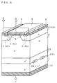
- Fig. 6 is a cross sectional view showing the structure of an IGBT according to a fourth preferred embodiment of the present invention.
- Omission of the buffer layer 21 in the device of the fourth preferred embodiment is a difference between the device of the fourth preferred embodiment and the device of the first preferred embodiment shown in Fig. 1.
- the heavily doped n-type semiconductor region 22 is selectively disposed between the n-type semiconductor layer 3 and the p-type semiconductor layer 1.
- the n-type semiconductor layer 3 and the heavily doped n-type semiconductor region 22 respectively have the same n-type impurity concentrations as those of the equivalent layer and region of the first preferred embodiment.
- the n-type semiconductor layer 3 and the p-type semiconductor layer 1 are directly joined to each other without an interposed heavily doped n-type semiconductor layer.
- the n-type semiconductor layer 3 is formed to have a sufficiently large thickness z.
- the n-type semiconductor layer 3 which is relatively lightly doped n-type and the n-type semiconductor region 22 which is relatively heavily doped n-type are arranged parallel with each other on the top surface of the p-type semiconductor layer 1. This reduces the ON-resistance and the collector current I C in the large forward current region lower than those in the conventional device.
- the device of the fourth preferred embodiment is designed so as to have an ON-voltage which is equal to that of the conventional device, a further lower collector current I C in the large forward current region than that in the conventional device is attained.
- the current capacity around the normal rated current of the fourth preferred embodiment is increased and the ON-resistance is suppressed even lower as compared with the conventional device.
- Fig. 7 is a cross sectional view showing the structure of an IGBT according to a fifth preferred embodiment of the present invention.
- the device according to the fifth preferred embodiment is different from the device of the first preferred embodiment in terms of the structure of an upper portion of the n-type semiconductor layer 3.
- the device of the fifth preferred embodiment known as an U-type IGBT, is advantageous over the devices of the preceding embodiments since it can be formed denser in an easy manner.
- the p-type base region 4 can be formed on the entire top major surface of the n-type semiconductor layer 11 during fabrication and therefore there is no need for selectively forming the p-type base region 4, manufacturing of the device is less complex.
- the p-type base region 4 and the n-type emitter region 5 are formed in the top surface of the n-type semiconductor layer 3.
- a groove 31 is also formed in the top surface of the n-type semiconductor layer 3 so that the side walls of the groove 31 extend across the n-type emitter region 5, the p-type base region 4 and into the n-type semiconductor layer 3.
- a gate insulation film 32 (insulating layer) is disposed.
- a gate electrode 33 made of polysilicon (control electrode layer) is buried inside the insulation film 32.
- the device of the fifth preferred embodiment is similar to the devices of the preceding preferred embodiments in that the gate electrode 33 is disposed facing the surface of the p-type base region 4.
- the p-type base region 4 With application of the gate voltage V GE of a predetermined value, the p-type base region 4 is inverted into the n-type at a channel region 35 which is formed in the vicinity of the gate electrode 33, creating an n-type channel at the channel region 35.
- Carriers in this case electrons, are introduced from the emitter electrode 9 into the n-type semiconductor layer 3 through this channel, thereby turning on the device. That is, the device of the fifth preferred embodiment operates in a way similar to the device of the first preferred embodiment. In terms of the ranges of concentration of the n-type impurities in the buffer layer 21 and the heavily doped n-type semiconductor region 22, the fifth preferred embodiment is similar to the first preferred embodiment.
- the buffer layer 21 of a relatively low n-type impurity concentration and the n-type semiconductor region 22 of a relatively high n-type impurity concentration are arranged parallel with each other between the n-type semiconductor layer 3 and the p-type semiconductor layer 1.
- the ON-resistance and the collector current I C in the large forward current region are suppressed to be low.
- the device of the fifth preferred embodiment is designed so as to have an ON-current which is equal to that of the conventional device, a further lower collector current I C in the large forward current region than that in the conventional device is attained.
- the current capacity around the normal rated current of the fifth preferred embodiment is increased and the ON-resistance is suppressed even lower as compared with the conventional device.
- Fig. 8 is a cross sectional view showing the structure of the IGBT according to a sixth preferred embodiment of the present invention.
- the heavily doped n-type semiconductor region 22 is formed in a different configuration from that of the device of the first preferred embodiment.
- the heavily doped n-type semiconductor region 22 is formed as two portions which are spaced apart from each other in one unit cell. In this this embodiment, however, the heavily doped n-type semiconductor region 22a is formed as one integrated portion in one unit cell.
- the heavily doped n-type semiconductor region is disposed as a continued region right below approximately the whole p-type base region 4 to have a gap right below the n-type semiconductor layer which separates the two portions 4a and 4b of the p-type base region 4.
- the device of this embodiment also functions as the device of the first preferred embodiment and has similar effects.
- Fig. 9 is a cross sectional perspective view showing the structure of the IGBT according to a seventh preferred embodiment of the present invention.
- the heavily doped n-type semiconductor region 22 is disposed in a different direction from the heavily doped n-type semiconductor region 22 of the device of the first preferred embodiment.
- the p-type base region 4 formed in the shape of stripes in the top major surface of the n-type semiconductor layer 11 runs parallel to the heavily doped n-type semiconductor region 22 which is also formed in the shape of stripes.
- the heavily doped n-type semiconductor region 22b runs perpendicular to the p-type base region 4.
- a positional relation between the gaps of the heavily doped n-type semiconductor region 22 and the gaps of the p-type base region 4 affects the characteristics of the device. To deal with this, the positional relation must be adjusted accurately if not very strictly accurately. In the device of this embodiment, however, since the heavily doped n-type semiconductor region 22b and the p-type base region 4 are disposed in intersecting directions, a positional relation between the two can be decided with no restriction. This eliminates the necessity of accurately aligning the mask pattern for formation of the heavily doped n-type semiconductor region 22 during fabrication of the device, which makes the fabrication simple. In addition, the characteristics of the device would not vary among products.
- Fig. 9 shows an example where the p-type base region 4 and the heavily doped n-type semiconductor region 22b run perpendicular to each other, as far as being disposed in directions which cross each other with a certain angle, the same effects are attainable.
- Figs. 10 to 12 are plan views of three different configurations each in the interface between the p-type semiconductor layer 1 and the n-type semiconductor layer 11.
- Fig. 10 shows the configuration of the heavily doped n-type semiconductor region 22 in the seventh preferred embodiment of Fig. 9, namely, the heavily doped n-type semiconductor region 22b which are in the form of parallel stripes.
- the heavily doped n-type semiconductor region 22 of Fig. 1 and the like has a similar configuration.
- the heavily doped n-type semiconductor region 22a shown in Fig. 8 is in a similar configuration, the width and the pitch of the stripes are different.
- the heavily doped n-type semiconductor region 22c shown in Fig. 11 includes a plurality of small square regions which are arranged with a space from each other in a matrix.
- the small regions may not be square.
- the heavily doped n-type semiconductor region 22d shown in Fig. 12 is somewhat similar to the heavily doped n-type semiconductor region 22c and the p-type semiconductor layer 1 of Fig. 11 replaced to each other.
- the heavily doped n-type semiconductor region 22d is in the form of a lattice or cross stripes which includes square openings. The openings may not be square.
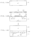
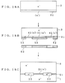
- Figs. 13A to 13C are cross sectional views showing the device of the first preferred embodiment (Fig. 1) during successive stages of fabrication.
- a first step of manufacturing the device of the first preferred embodiment is preparation of a p-type silicon substrate which corresponds to the p-type collector layer 1 (Fig. 13A).
- the p-type collector layer 1 is covered at the entire top major surface with a resist layer from which a resist pattern 51 (shielding film) will be subsequently formed by a photolithography process through a mask 61.
- n-type impurities such as As are selectively implanted through the pattern 51, thereby defining an n-type semiconductor region 41 in the top surface of the p-type semiconductor layer 1 (Fig. 21B).
- the buffer layer 21 is then epitaxially grown on the p-type semiconductor layer 1, in the course of which the n-type impurities of the n-type semiconductor region 41 diffuse outside to thereby define the heavily doped n-type semiconductor region 22 between the buffer layer 21 and the p-type semiconductor layer 1.
- the n-type semiconductor layer 3 is then epitaxially grown on the buffer layer 21 (Fig. 21C).
- the device of the first preferred embodiment is hereinafter manufactured using conventional processing techniques. More particularly, the top surface of the n-type semiconductor layer 3 is locally doped to form the p-type base region 4 and the n-type emitter region 5 thereat. Then, the gate insulation film 7, the gate electrode 8 and the emitter electrode 9 are connected. Further, the collector electrode 10 is connected to the bottom major surface of the p-type semiconductor layer 1 (Fig. 1).
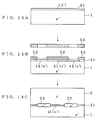
- Figs. 14A to 14C are cross sectional views showing the device of the second preferred embodiment (Fig. 4) during successive stages of fabrication.
- a p-type silicon substrate which corresponds to the p-type collector layer 1 is prepared.
- the buffer layer 21 is formed on the p-type collector layer 1 by epitaxial growth.
- the buffer layer 21 is formed to a thickness which does not exceed the thickness of the heavily doped n-type semiconductor region 22 which will be formed later (Fig. 14A).
- a resist layer is then formed entirely over the top major surface of the p-type collector layer 1 and patterned through a mask 62 by a photolithography process to thereby define a resist pattern 52 (shielding film).
- n-type impurities such as As are selectively implanted through the resist pattern 52, thereby defining an n-type semiconductor region 42 in the top surface of the buffer layer 21 (Fig. 14B).
- the resist pattern 52 is then removed, followed by epitaxial growth of the n-type semiconductor layer 3 on the buffer layer 21.
- the n-type impurities of the n-type semiconductor region 42 diffuse into the n-type semiconductor layer 3 and p-type collector layer 1 while the layer 3 is epitaxially grown so that the heavily doped n-type semiconductor region 22 is formed between the n-type semiconductor layer 3 and the p-type semiconductor layer 1 (Fig. 14C).
- the device shown in Fig. 4 is hereinafter completed by procedures similar to those used to fabricate the device of the first preferred embodiment.
- Figs. 15A to 15C are cross sectional views showing the device of the third preferred embodiment (Fig. 5) during successive stages of fabrication.
- a p-type silicon substrate which corresponds to the p-type collector layer 1 is prepared.
- the buffer layer 21 is formed on the p-type collector layer 1 by epitaxial growth.
- the buffer layer 21 is formed to a thickness which is sufficiently larger than the thickness of the heavily doped n-type semiconductor region 22 which will be formed later (Fig. 15A).
- the buffer layer 21 is covered at the entire top major surface with a resist layer from which a resist pattern 53 (shielding film) will be subsequently formed by a photolithography process through a mask 63.
- n-type impurities such as As are selectively implanted through the resist pattern 53, thereby defining an n-type semiconductor region 43 in the top surface of the buffer layer 21 (Fig. 15B).
- the resist pattern 53 is then removed, followed by epitaxial growth of the n-type semiconductor layer 3 on the buffer layer 21.
- the n-type impurities of the n-type semiconductor region 43 diffuse into the n-type semiconductor layer 3 and the buffer layer 21 while the layer is epitaxially grown so that the heavily doped n-type semiconductor region 22 is formed between the n-type semiconductor layer 3 and the buffer layer 21 (Fig. 15C).
- the device shown in Fig. 5 is hereinafter completed by procedures similar to those used to fabricate the device of the first preferred embodiment.
- Figs. 16A to 16C are cross sectional views showing the device of the fourth preferred embodiment (Fig. 6) during successive stages of fabrication. It is to be noted that Figs. 16A to 16C illustrate the device upside down to as it regularly is during fabrication so as to be in conformity with Fig. 6 which shows a cross section of the finished device.
- Fig. 16A an n-type silicon substrate which corresponds to the n-type semiconductor layer 3 is prepared (Fig. 16A).
- the n-type semiconductor layer 3 is covered at the entire bottom major surface with a resist layer from which a resist pattern 54 (shielding film) will be subsequently formed by a photolithography process through a mask 64.
- n-type impurities such as As are selectively implanted through the resist pattern 54, thereby defining an n-type semiconductor region 44 in the bottom surface of the n-type semiconductor layer 3 (Fig. 16B).
- the resist pattern 54 is then removed, and the p-type semiconductor layer 1 is epitaxially grown on the bottom major surface of the n-type semiconductor layer 3.
- the n-type impurities of the n-type semiconductor region 44 diffuse, whereby the heavily doped n-type semiconductor region 22 is formed between the n-type semiconductor layer 3 and the p-type semiconductor layer 1 (Fig. 16C).
- the device shown in Fig. 6 will be hereinafter completed by procedures similar to those used to fabricate the device of the first preferred embodiment.
- the semiconductor substrate which corresponds to the n-type semiconductor layer 3 is prepared first instead of forming the p-type semiconductor layer 1 as in the preceding methods is because the n-type semiconductor layer 3 must be sufficiently thick to manufacture the device of the fourth preferred embodiment.
- formation of the n-type semiconductor layer 3 by expensive epitaxial growth contradicts economies in production.
- the p-type semiconductor layer 1 may be prepared first and the n-type semiconductor layer 3 may be formed by epitaxial growth to manufacture the device shown in Fig. 6.
- Fabrication of the device of the fifth preferred embodiment is similar to that explained as the sixth preferred embodiment up to formation of the heavily doped n-type semiconductor region 22.
- the procedures that follow are similar to procedures conventionally used in fabrication of a U-type IGBT.
- the devices according to the first to the third and the fifth preferred embodiments are also obtainable by preparing the n-type semiconductor layer 3 first instead of the p-type semiconductor layer 1, which is similar to the manufacturing process of the fourth preferred embodiment. In the following such a manufacturing method will be described.
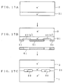
- Figs. 17A to 17C are views showing the device of the first preferred embodiment (Fig. 1) during successive stages of other type of fabrication. Like Figs. 16A to 16C, Figs. 17A to 17C illustrate the device upside down to as it regularly is during fabrication so as to be in conformity with Fig. 1 which shows a cross section of the finished device. For the sake of convenience, Figs. 17A to 17C will be referred to here. This is also the same regarding Figs. 18A to 18C and Figs. 19A to 19C.
- an n-type silicon substrate which corresponds to the n-type semiconductor layer 3 is prepared first.
- the buffer layer 21 is epitaxially grown.
- the buffer layer 21 is formed so as to be sufficiently thicker than the heavily doped n-type semiconductor region 22 described later (Fig. 17A).
- a resist layer is formed all over a bottom major surface of the buffer layer 21 and photolithography patterned using the mask 61, thereby defining the resist pattern 51 (shielding film).
- n-type impurities such as As are selectively injected so that the n-type semiconductor region 41 is selectively formed in the bottom major surface of the buffer layer 21 (Fig. 17B).
- the resist pattern 51 is removed and the p-type semiconductor layer 1 is epitaxially grown on bottom major surface of the buffer layer 21.
- the n-type impurities diffuse from the n-type semiconductor region 41, whereby the heavily doped n-type semiconductor region 22 is formed between the p-type semiconductor layer 1 and the fubber layer 21 (Fig. 17C).
- the impurity concentration of the n-type impurities in the n-type semiconductor layer 3 needs be accurately adjusted, the impurity concentration of the p-type impurities in the p-type semiconductor layer 1 may not be adjusted very accurately.
- the n-type semiconductor layer 3 which requires relatively accurate adjustment is prepared in advance as a substrate and the p-type semiconductor layer 1 which does not require very accurate adjustment is epitaxially grown, and therefore, it is easy to correctly adjust the impurity concentration of the n-type impurities in the n-type semiconductor layer 3.
- the p-type semiconductor layer 1 is formed easily.
- Fig. 18A to 18C are views showing the device of the second preferred embodiment (Fig. 4) during successive stages of other type of fabrication.
- this manufacturing method first, an n-type silicon substrate which corresponds to the n-type semiconductor layer 3 is prepared. Next, on a bottom major surface of the n-type semiconductor layer 3, the buffer layer 21 is epitaxially grown. The buffer layer 21 is formed so as to be thinner than the heavily doped n-type semiconductor region 22 described later (Fig. 18A).
- a resist layer is formed all over a bottom major surface of the buffer layer 21 and photolithography patterned using the mask 62, thereby defining the resist pattern 52 (shielding film).
- n-type impurities such as As are selectively injected so that the n-type semiconductor region 42 is selectively formed in the bottom major surface of the buffer layer 21 (Fig. 18B).
- the resist pattern 52 is removed and the p-type semiconductor layer 1 is epitaxially grown on bottom major surface of the buffer layer 21.
- the n-type impurities diffuse from the n-type semiconductor region 42, whereby the heavily doped n-type semiconductor region 22 is formed between the p-type semiconductor layer 1 and the fubber layer 21 (Fig. 18C).
- the device shown in Fig. 4 is fabricated.
- the n-type semiconductor layer 3 which requires relatively accurate adjustment is prepared in advance as a substrate and the p-type semiconductor layer 1 which does not require very accurate adjustment is epitaxially grown, and therefore, it is easy to correctly adjust the impurity concentration of the n-type impurities in the n-type semiconductor layer 3 and to form the p-type semiconductor layer 1.
- Fig. 19A to 19C are views showing the device of the third preferred embodiment (Fig. 5) during successive stages of other type of fabrication.
- this manufacturing method first, an n-type silicon substrate which corresponds to the n-type semiconductor layer 3 is prepared (Fig. 19A).
- a resist layer is grown on the entire bottom major surface of the n-type semiconductor layer 3 and photolithography patterned using the mask 63, thereby defining the resist pattern 53 (shielding film).
- n-type impurities such as As are selectively injected so that the n-type semiconductor region 43 is selectively formed in the bottom major surface of the n-type semiconductor layer 3 (Fig. 19B).
- the buffer layer 21 is epitaxially grown on the bottom major surface of the n-type semiconductor layer 3. During this epitaxial growth, the n-type impurities diffuse from the n-type semiconductor region 43, whereby the heavily doped n-type semiconductor region 22 is formed between the buffer layer 21 and the n-type semiconductor layer 3.
- the buffer layer 21 is formed so as to be sufficiently thick so that the heavily doped n-type semiconductor region 22 will not extend to the bottom major surface of the buffer layer 21.
- the p-type semiconductor layer 1 is epitaxially grown on the bottom major surface of the buffer layer 21 (Fig. 19C).
- the device shown in Fig. 5 is obtained.
- the n-type semiconductor layer 3 which requires relatively accurate adjustment is prepared in advance as a substrate and the p-type semiconductor layer 1 which does not require very accurate adjustment is epitaxially grown, and therefore, it is easy to correctly adjust the impurity concentration of the n-type impurities in the n-type semiconductor layer 3 and to form the p-type semiconductor layer 1.
- FIG. 7 Other manufacturing method of the device of the fifth preferred embodiment (Fig. 7) is similar to the processes (Figs. 17A to 17C) of the fourteenth preferred embodiment up to formation of the heavily doped n-type semiconductor region 22.
- the subsequent processes are the same as conventional processes for fabrication of an U-type IGBT.
- the n-type semiconductor layer 3 which requires relatively accurate adjustment is prepared in advance as a substrate and the p-type semiconductor layer 1 which does not require very accurate adjustment is epitaxially grown, and therefore, it is easy to correctly adjust the impurity concentration of the n-type impurities in the n-type semiconductor layer 3 and to form the p-type semiconductor layer 1.
- the present invention is also applicable to a p-channel IGBT in which the semiconductor layers of alternate conductivity are disposed in an opposite manner to that of an n-channel IGBT.
- the present invention can be applied to other types of insulated gate semiconductor devices such as ESTs and MCTs.
Landscapes
- Engineering & Computer Science (AREA)
- Microelectronics & Electronic Packaging (AREA)
- Power Engineering (AREA)
- Physics & Mathematics (AREA)
- Ceramic Engineering (AREA)
- Condensed Matter Physics & Semiconductors (AREA)
- General Physics & Mathematics (AREA)
- Computer Hardware Design (AREA)
- Manufacturing & Machinery (AREA)
- Insulated Gate Type Field-Effect Transistor (AREA)
- Thyristors (AREA)
- Bipolar Transistors (AREA)
Applications Claiming Priority (6)
| Application Number | Priority Date | Filing Date | Title |
|---|---|---|---|
| JP28166492 | 1992-10-20 | ||
| JP28166492 | 1992-10-20 | ||
| JP281664/92 | 1992-10-20 | ||
| JP23499293 | 1993-09-21 | ||
| JP234992/93 | 1993-09-21 | ||
| JP05234992A JP3081739B2 (ja) | 1992-10-20 | 1993-09-21 | 絶縁ゲート型半導体装置及びその製造方法 |
Publications (2)
| Publication Number | Publication Date |
|---|---|
| EP0594049A1 true EP0594049A1 (de) | 1994-04-27 |
| EP0594049B1 EP0594049B1 (de) | 2002-01-30 |
Family
ID=26531893
Family Applications (1)
| Application Number | Title | Priority Date | Filing Date |
|---|---|---|---|
| EP93116565A Expired - Lifetime EP0594049B1 (de) | 1992-10-20 | 1993-10-13 | Bipolarer Transistor mit isolierter Steuerelektrode und Verfahren zur Herstellung desselben |
Country Status (4)
| Country | Link |
|---|---|
| US (1) | US5569941A (de) |
| EP (1) | EP0594049B1 (de) |
| JP (1) | JP3081739B2 (de) |
| DE (1) | DE69331512T2 (de) |
Cited By (10)
| Publication number | Priority date | Publication date | Assignee | Title |
|---|---|---|---|---|
| EP0725446A1 (de) * | 1995-02-02 | 1996-08-07 | Motorola, Inc. | Bipolare Halbleiteranordnung mit isolierter Gateelektrode und Verfahren zur Herstellung |
| FR2731841A1 (fr) * | 1995-03-07 | 1996-09-20 | Nippon Denso Co | Transistors a effet de champ du type a grille isolee et son procede de fabrication |
| EP0746040A1 (de) * | 1995-05-31 | 1996-12-04 | Co.Ri.M.Me. Consorzio Per La Ricerca Sulla Microelettronica Nel Mezzogiorno | Verbesserte IGBT-Anordnung |
| EP0779662A2 (de) * | 1995-12-11 | 1997-06-18 | Mitsubishi Denki Kabushiki Kaisha | Halbleiterbauelement mit Bipolarstruktur und dessen Herstellungsverfahren |
| US5925911A (en) * | 1995-04-26 | 1999-07-20 | Nippondenso Co., Ltd. | Semiconductor device in which defects due to LOCOS or heat treatment are suppressed |
| US5981981A (en) * | 1993-10-13 | 1999-11-09 | Mitsubishi Denki Kabushiki Kaisha | Semiconductor device including a bipolar structure |
| US6271061B1 (en) | 1997-12-03 | 2001-08-07 | Stmicroelectronics S.R.L. | Fabrication of insulated gate bipolar devices |
| DE19644504B4 (de) * | 1996-05-16 | 2004-01-22 | Mitsubishi Denki K.K. | Halbleitervorrichtung mit hoher Durchbruchspannung und Verfahren zu deren Herstellung |
| WO2004030103A1 (de) * | 2002-09-20 | 2004-04-08 | Infineon Technologies Ag | Verfahren zur herstellung einer vergrabenen stoppzone in einem halbleiterbauelement und halbleiterbauelement mit einer vergrabenen stoppzone |
| US7675108B2 (en) | 2004-08-12 | 2010-03-09 | Infineon Technologies Ag | Method for producing a buried N-doped semiconductor zone in a semiconductor body and semiconductor component |
Families Citing this family (36)
| Publication number | Priority date | Publication date | Assignee | Title |
|---|---|---|---|---|
| KR0163875B1 (ko) * | 1994-11-30 | 1998-12-01 | 윤종용 | 반도체장치 및 그 제조방법 |
| GB2327295A (en) * | 1997-07-11 | 1999-01-20 | Plessey Semiconductors Ltd | MOS controllable power semiconductor device |
| US6081009A (en) * | 1997-11-10 | 2000-06-27 | Intersil Corporation | High voltage mosfet structure |
| SE9704149D0 (sv) * | 1997-11-13 | 1997-11-13 | Abb Research Ltd | A semiconductor device of SiC and a transistor of SiC having an insulated gate |
| DE19820956A1 (de) * | 1998-05-11 | 1999-11-18 | Daimler Chrysler Ag | Halbleiter-Bauelement und Verfahren zu seiner Herstellung sowie Verwendung des Halbleiter-Bauelements |
| JP2002530869A (ja) * | 1998-11-18 | 2002-09-17 | インフィネオン テクノロジース アクチエンゲゼルシャフト | 誘電性または半絶縁性シールド構造体を有する半導体構成素子 |
| JP4479041B2 (ja) * | 2000-03-10 | 2010-06-09 | 株式会社デンソー | 半導体装置及びその製造方法 |
| JP2002158278A (ja) | 2000-11-20 | 2002-05-31 | Hitachi Ltd | 半導体装置およびその製造方法ならびに設計方法 |
| JP3647802B2 (ja) * | 2001-01-25 | 2005-05-18 | 株式会社東芝 | 横型半導体装置 |
| JP4904625B2 (ja) * | 2001-02-14 | 2012-03-28 | 富士電機株式会社 | 半導体装置 |
| DE10214176B4 (de) * | 2002-03-28 | 2010-09-02 | Infineon Technologies Ag | Halbleiterbauelement mit einer vergrabenen Stoppzone und Verfahren zur Herstellung einer Stoppzone in einem Halbleiterbauelement |
| JP2006518107A (ja) * | 2003-02-18 | 2006-08-03 | コーニンクレッカ フィリップス エレクトロニクス エヌ ヴィ | 半導体装置及びそのような装置の製造方法 |
| DE10325721B4 (de) * | 2003-06-06 | 2009-02-05 | Infineon Technologies Ag | Halbleiterbauelement |
| DE10333556B4 (de) * | 2003-07-23 | 2006-07-06 | Infineon Technologies Ag | Halbleiterbauelement mit verbesserter Kommutierung |
| DE102004005084B4 (de) * | 2004-02-02 | 2013-03-14 | Infineon Technologies Ag | Halbleiterbauelement |
| US7687841B2 (en) * | 2005-08-02 | 2010-03-30 | Micron Technology, Inc. | Scalable high performance carbon nanotube field effect transistor |
| JP5201305B2 (ja) * | 2006-07-03 | 2013-06-05 | 富士電機株式会社 | 半導体装置の製造方法 |
| JP5036327B2 (ja) * | 2007-01-23 | 2012-09-26 | 三菱電機株式会社 | 半導体装置及びその製造方法 |
| EP2330617A4 (de) | 2008-09-01 | 2012-01-25 | Rohm Co Ltd | Halbleiterbauelement und herstellungsverfahren dafür |
| CN102637724A (zh) * | 2012-03-31 | 2012-08-15 | 上海宏力半导体制造有限公司 | 绝缘栅双极型晶体管 |
| US20130277793A1 (en) | 2012-04-24 | 2013-10-24 | Fairchild Korea Semiconductor, Ltd. | Power device and fabricating method thereof |
| US9685335B2 (en) * | 2012-04-24 | 2017-06-20 | Fairchild Korea Semiconductor Ltd. | Power device including a field stop layer |
| KR102155721B1 (ko) * | 2013-06-27 | 2020-09-15 | 온세미컨덕터코리아 주식회사 | 파워 소자 및 그의 제조 방법 |
| US10181513B2 (en) | 2012-04-24 | 2019-01-15 | Semiconductor Components Industries, Llc | Power device configured to reduce electromagnetic interference (EMI) noise |
| JP6102092B2 (ja) * | 2012-06-22 | 2017-03-29 | サンケン電気株式会社 | 半導体装置及びその製造方法 |
| DE102013018789A1 (de) * | 2012-11-29 | 2014-06-05 | Infineon Technologies Ag | Steuern lichterzeugter Ladungsträger |
| USD729808S1 (en) * | 2013-03-13 | 2015-05-19 | Nagrastar Llc | Smart card interface |
| USD758372S1 (en) | 2013-03-13 | 2016-06-07 | Nagrastar Llc | Smart card interface |
| USD759022S1 (en) * | 2013-03-13 | 2016-06-14 | Nagrastar Llc | Smart card interface |
| DE102014009384A1 (de) * | 2013-06-27 | 2014-12-31 | Fairchild Korea Semiconductor Ltd. | Leistungsvorrichtung und Verfahren zur Herstellung selbiger |
| CN105428404B (zh) * | 2014-06-17 | 2021-02-19 | 快捷韩国半导体有限公司 | 功率器件及其制造方法 |
| USD780763S1 (en) * | 2015-03-20 | 2017-03-07 | Nagrastar Llc | Smart card interface |
| USD864968S1 (en) * | 2015-04-30 | 2019-10-29 | Echostar Technologies L.L.C. | Smart card interface |
| CN106252399B (zh) * | 2016-08-31 | 2019-03-29 | 电子科技大学 | 一种逆导型igbt |
| US11069769B2 (en) * | 2017-09-07 | 2021-07-20 | Mitsubishi Electric Corporation | Semiconductor device |
| JP7513554B2 (ja) * | 2021-03-11 | 2024-07-09 | 株式会社東芝 | 半導体装置 |
Citations (5)
| Publication number | Priority date | Publication date | Assignee | Title |
|---|---|---|---|---|
| JPS61216363A (ja) * | 1985-03-22 | 1986-09-26 | Toshiba Corp | 伝導度変調型半導体装置 |
| JPH023288A (ja) * | 1988-06-20 | 1990-01-08 | Meidensha Corp | 絶縁ゲート型バイポーラトランジスタ |
| EP0450082A1 (de) * | 1989-08-31 | 1991-10-09 | Nippondenso Co., Ltd. | Bipolarer transistor mit isolierter steuerelektrode |
| DE4112905A1 (de) * | 1990-04-20 | 1991-10-24 | Fuji Electric Co Ltd | Leitfaehigkeitsmodulations-mosfet und verfahren zu seiner herstellung |
| EP0503605A2 (de) * | 1991-03-12 | 1992-09-16 | Nippondenso Co., Ltd. | Bipolarer Transistor vom isolierten Gatetyp mit Überspannungschutz |
Family Cites Families (8)
| Publication number | Priority date | Publication date | Assignee | Title |
|---|---|---|---|---|
| US4672407A (en) * | 1984-05-30 | 1987-06-09 | Kabushiki Kaisha Toshiba | Conductivity modulated MOSFET |
| JPS62283669A (ja) * | 1986-06-02 | 1987-12-09 | Toshiba Corp | 導電変調型mosfet |
| JPS63288064A (ja) * | 1987-05-20 | 1988-11-25 | Toshiba Corp | 複合サイリスタ |
| JPH01282872A (ja) * | 1988-05-09 | 1989-11-14 | Matsushita Electron Corp | 半導体装置 |
| EP0405200A1 (de) * | 1989-06-30 | 1991-01-02 | Asea Brown Boveri Ag | MOS-gesteuertes, bipolares Leistungshalbleiter-Bauelement |
| EP0416805B1 (de) * | 1989-08-30 | 1996-11-20 | Siliconix, Inc. | Transistor mit Spannungsbegrenzungsanordnung |
| US5202750A (en) * | 1990-04-09 | 1993-04-13 | U.S. Philips Corp. | MOS-gated thyristor |
| JPH0472669A (ja) * | 1990-05-10 | 1992-03-06 | Fuji Electric Co Ltd | 絶縁ゲート型バイポーラトランジスタ |
-
1993
- 1993-09-21 JP JP05234992A patent/JP3081739B2/ja not_active Expired - Fee Related
- 1993-10-13 EP EP93116565A patent/EP0594049B1/de not_active Expired - Lifetime
- 1993-10-13 DE DE69331512T patent/DE69331512T2/de not_active Expired - Fee Related
-
1995
- 1995-05-16 US US08/441,787 patent/US5569941A/en not_active Expired - Fee Related
Patent Citations (5)
| Publication number | Priority date | Publication date | Assignee | Title |
|---|---|---|---|---|
| JPS61216363A (ja) * | 1985-03-22 | 1986-09-26 | Toshiba Corp | 伝導度変調型半導体装置 |
| JPH023288A (ja) * | 1988-06-20 | 1990-01-08 | Meidensha Corp | 絶縁ゲート型バイポーラトランジスタ |
| EP0450082A1 (de) * | 1989-08-31 | 1991-10-09 | Nippondenso Co., Ltd. | Bipolarer transistor mit isolierter steuerelektrode |
| DE4112905A1 (de) * | 1990-04-20 | 1991-10-24 | Fuji Electric Co Ltd | Leitfaehigkeitsmodulations-mosfet und verfahren zu seiner herstellung |
| EP0503605A2 (de) * | 1991-03-12 | 1992-09-16 | Nippondenso Co., Ltd. | Bipolarer Transistor vom isolierten Gatetyp mit Überspannungschutz |
Non-Patent Citations (2)
| Title |
|---|
| PATENT ABSTRACTS OF JAPAN vol. 11, no. 55 (E - 481)<2502> 20 February 1987 (1987-02-20) * |
| PATENT ABSTRACTS OF JAPAN vol. 14, no. 139 (E - 903) 15 March 1990 (1990-03-15) * |
Cited By (14)
| Publication number | Priority date | Publication date | Assignee | Title |
|---|---|---|---|---|
| US5981981A (en) * | 1993-10-13 | 1999-11-09 | Mitsubishi Denki Kabushiki Kaisha | Semiconductor device including a bipolar structure |
| EP0725446A1 (de) * | 1995-02-02 | 1996-08-07 | Motorola, Inc. | Bipolare Halbleiteranordnung mit isolierter Gateelektrode und Verfahren zur Herstellung |
| FR2731841A1 (fr) * | 1995-03-07 | 1996-09-20 | Nippon Denso Co | Transistors a effet de champ du type a grille isolee et son procede de fabrication |
| US5925911A (en) * | 1995-04-26 | 1999-07-20 | Nippondenso Co., Ltd. | Semiconductor device in which defects due to LOCOS or heat treatment are suppressed |
| EP0746040A1 (de) * | 1995-05-31 | 1996-12-04 | Co.Ri.M.Me. Consorzio Per La Ricerca Sulla Microelettronica Nel Mezzogiorno | Verbesserte IGBT-Anordnung |
| EP0779662A2 (de) * | 1995-12-11 | 1997-06-18 | Mitsubishi Denki Kabushiki Kaisha | Halbleiterbauelement mit Bipolarstruktur und dessen Herstellungsverfahren |
| EP0779662A3 (de) * | 1995-12-11 | 1997-11-05 | Mitsubishi Denki Kabushiki Kaisha | Halbleiterbauelement mit Bipolarstruktur und dessen Herstellungsverfahren |
| DE19644504B4 (de) * | 1996-05-16 | 2004-01-22 | Mitsubishi Denki K.K. | Halbleitervorrichtung mit hoher Durchbruchspannung und Verfahren zu deren Herstellung |
| US6271061B1 (en) | 1997-12-03 | 2001-08-07 | Stmicroelectronics S.R.L. | Fabrication of insulated gate bipolar devices |
| WO2004030103A1 (de) * | 2002-09-20 | 2004-04-08 | Infineon Technologies Ag | Verfahren zur herstellung einer vergrabenen stoppzone in einem halbleiterbauelement und halbleiterbauelement mit einer vergrabenen stoppzone |
| US7361970B2 (en) | 2002-09-20 | 2008-04-22 | Infineon Technologies Ag | Method for production of a buried stop zone in a semiconductor component and semiconductor component comprising a buried stop zone |
| US7749876B2 (en) | 2002-09-20 | 2010-07-06 | Infineon Technologies Ag | Method for the production of a buried stop zone in a semiconductor component and semiconductor component comprising a buried stop zone |
| US7675108B2 (en) | 2004-08-12 | 2010-03-09 | Infineon Technologies Ag | Method for producing a buried N-doped semiconductor zone in a semiconductor body and semiconductor component |
| US8101506B2 (en) | 2004-08-12 | 2012-01-24 | Infineon Technologies Ag | Method for producing a buried n-doped semiconductor zone in a semiconductor body and semiconductor component |
Also Published As
| Publication number | Publication date |
|---|---|
| EP0594049B1 (de) | 2002-01-30 |
| DE69331512D1 (de) | 2002-03-14 |
| JP3081739B2 (ja) | 2000-08-28 |
| JPH06204481A (ja) | 1994-07-22 |
| DE69331512T2 (de) | 2002-09-12 |
| US5569941A (en) | 1996-10-29 |
Similar Documents
| Publication | Publication Date | Title |
|---|---|---|
| EP0594049B1 (de) | Bipolarer Transistor mit isolierter Steuerelektrode und Verfahren zur Herstellung desselben | |
| US11923444B2 (en) | Semiconductor device and manufacturing method of semiconductor device | |
| USRE38953E1 (en) | Insulated gate semiconductor device and method of manufacturing the same | |
| JP2504862B2 (ja) | 半導体装置及びその製造方法 | |
| US5324966A (en) | MOS-controlled thyristor | |
| EP0424710B1 (de) | Thyristor und Verfahren zu dessen Herstellung | |
| US10797131B2 (en) | Enhancements to cell layout and fabrication techniques for MOS-gated devices | |
| KR100880231B1 (ko) | 반도체 소자 및 그의 제조 방법 | |
| US5981981A (en) | Semiconductor device including a bipolar structure | |
| EP0779662B1 (de) | Halbleiterbauelement mit Bipolarstruktur und dessen Herstellungsverfahren | |
| EP1104027B1 (de) | Leistungshalbleiteranordnung mit einem Ballastwiderstandsbereich | |
| US5525816A (en) | Insulated gate semiconductor device with stripe widths | |
| US5281833A (en) | Insulated gate control thyristor | |
| KR0163875B1 (ko) | 반도체장치 및 그 제조방법 | |
| US5397716A (en) | Method of forming an insulated gate semiconductor device | |
| US5624855A (en) | Process of producing insulated-gate bipolar transistor | |
| EP0540017A1 (de) | MOS-Gate-kontrollierter Thyristor | |
| US5223732A (en) | Insulated gate semiconductor device with reduced based-to-source electrode short | |
| JPH0555583A (ja) | 絶縁ゲート型バイポーラトランジスタの製造方法 | |
| KR100286045B1 (ko) | 버퍼층을 포함하는 반도체 장치 및 그 제조 방법 | |
| KR100269631B1 (ko) | 반도체장치의 인슐레이티드 게이트 바이폴라 트랜지스터 및 그 제조방법 | |
| KR100486350B1 (ko) | 에미터스위치사이리스터및이의제조방법 | |
| JPH05121746A (ja) | 絶縁ゲート形電界効果トランジスタ | |
| JPH0794724A (ja) | 絶縁ゲートバイポーラトランジスタとその製造方法 |
Legal Events
| Date | Code | Title | Description |
|---|---|---|---|
| PUAI | Public reference made under article 153(3) epc to a published international application that has entered the european phase |
Free format text: ORIGINAL CODE: 0009012 |
|
| AK | Designated contracting states |
Kind code of ref document: A1 Designated state(s): DE FR GB |
|
| 17P | Request for examination filed |
Effective date: 19940909 |
|
| 17Q | First examination report despatched |
Effective date: 19951206 |
|
| GRAG | Despatch of communication of intention to grant |
Free format text: ORIGINAL CODE: EPIDOS AGRA |
|
| GRAG | Despatch of communication of intention to grant |
Free format text: ORIGINAL CODE: EPIDOS AGRA |
|
| GRAH | Despatch of communication of intention to grant a patent |
Free format text: ORIGINAL CODE: EPIDOS IGRA |
|
| GRAH | Despatch of communication of intention to grant a patent |
Free format text: ORIGINAL CODE: EPIDOS IGRA |
|
| GRAA | (expected) grant |
Free format text: ORIGINAL CODE: 0009210 |
|
| REG | Reference to a national code |
Ref country code: GB Ref legal event code: IF02 |
|
| AK | Designated contracting states |
Kind code of ref document: B1 Designated state(s): DE FR GB |
|
| REF | Corresponds to: |
Ref document number: 69331512 Country of ref document: DE Date of ref document: 20020314 |
|
| ET | Fr: translation filed | ||
| PLBE | No opposition filed within time limit |
Free format text: ORIGINAL CODE: 0009261 |
|
| STAA | Information on the status of an ep patent application or granted ep patent |
Free format text: STATUS: NO OPPOSITION FILED WITHIN TIME LIMIT |
|
| 26N | No opposition filed | ||
| PGFP | Annual fee paid to national office [announced via postgrant information from national office to epo] |
Ref country code: DE Payment date: 20061005 Year of fee payment: 14 |
|
| PGFP | Annual fee paid to national office [announced via postgrant information from national office to epo] |
Ref country code: GB Payment date: 20061011 Year of fee payment: 14 |
|
| GBPC | Gb: european patent ceased through non-payment of renewal fee |
Effective date: 20071013 |
|
| PG25 | Lapsed in a contracting state [announced via postgrant information from national office to epo] |
Ref country code: DE Free format text: LAPSE BECAUSE OF NON-PAYMENT OF DUE FEES Effective date: 20080501 |
|
| REG | Reference to a national code |
Ref country code: FR Ref legal event code: ST Effective date: 20080630 |
|
| PGFP | Annual fee paid to national office [announced via postgrant information from national office to epo] |
Ref country code: FR Payment date: 20061010 Year of fee payment: 14 |
|
| PG25 | Lapsed in a contracting state [announced via postgrant information from national office to epo] |
Ref country code: GB Free format text: LAPSE BECAUSE OF NON-PAYMENT OF DUE FEES Effective date: 20071013 |
|
| PG25 | Lapsed in a contracting state [announced via postgrant information from national office to epo] |
Ref country code: FR Free format text: LAPSE BECAUSE OF NON-PAYMENT OF DUE FEES Effective date: 20071031 |