EP0564280A2 - Schaltung zur Erzeugung einer Innenquellenspannung - Google Patents
Schaltung zur Erzeugung einer Innenquellenspannung Download PDFInfo
- Publication number
- EP0564280A2 EP0564280A2 EP93302561A EP93302561A EP0564280A2 EP 0564280 A2 EP0564280 A2 EP 0564280A2 EP 93302561 A EP93302561 A EP 93302561A EP 93302561 A EP93302561 A EP 93302561A EP 0564280 A2 EP0564280 A2 EP 0564280A2
- Authority
- EP
- European Patent Office
- Prior art keywords
- voltage
- vcc
- source voltage
- generating
- circuit
- Prior art date
- Legal status (The legal status is an assumption and is not a legal conclusion. Google has not performed a legal analysis and makes no representation as to the accuracy of the status listed.)
- Granted
Links
Images

Classifications
-
- G—PHYSICS
- G11—INFORMATION STORAGE
- G11C—STATIC STORES
- G11C11/00—Digital stores characterised by the use of particular electric or magnetic storage elements; Storage elements therefor
- G11C11/21—Digital stores characterised by the use of particular electric or magnetic storage elements; Storage elements therefor using electric elements
- G11C11/34—Digital stores characterised by the use of particular electric or magnetic storage elements; Storage elements therefor using electric elements using semiconductor devices
- G11C11/40—Digital stores characterised by the use of particular electric or magnetic storage elements; Storage elements therefor using electric elements using semiconductor devices using transistors
- G11C11/401—Digital stores characterised by the use of particular electric or magnetic storage elements; Storage elements therefor using electric elements using semiconductor devices using transistors forming cells needing refreshing or charge regeneration, i.e. dynamic cells
- G11C11/4063—Auxiliary circuits, e.g. for addressing, decoding, driving, writing, sensing or timing
- G11C11/407—Auxiliary circuits, e.g. for addressing, decoding, driving, writing, sensing or timing for memory cells of the field-effect type
-
- G—PHYSICS
- G11—INFORMATION STORAGE
- G11C—STATIC STORES
- G11C5/00—Details of stores covered by group G11C11/00
- G11C5/14—Power supply arrangements, e.g. power down, chip selection or deselection, layout of wirings or power grids, or multiple supply levels
- G11C5/147—Voltage reference generators, voltage or current regulators; Internally lowered supply levels; Compensation for voltage drops
Definitions
- the present invention relates to circuits for generating an internal source voltage - especially for semiconductor memory devices.
- a semiconductor memory device of 16 Mega bits or above should employ a circuit for generating an internal voltage to drop the level of the external voltage to the level of the operating voltage of the memory device.
- a semiconductor memory device of 16 Mega bits or above should use the internal voltage of 4V which is usually obtained by dropping the external voltage of 5V.
- Figure 1 of the accompanying diagrammatic drawings shows a circuit for generating an internal source voltage according to the prior art, and includes a reference voltage generating circuit 100 for generating a reference voltage Vref, a comparator 200 for comparing an internal source voltage int.Vcc with the reference voltage Vref, a driver 90 for driving an external voltage ext.Vcc to the internal source voltage int.Vcc under the control of the comparator 200, and a burn-in reference voltage generating circuit 300.
- the comparator 200 comprises NMOS transistors N1, N2, N3 and PMOS transistors P1, P2, connected between the external voltage ext.Vcc and ground voltage Vss.
- the internal source voltage int.Vcc is applied to the memory elements of the memory device as well as an NMOS transistor N2 of the comparator 200. If the internal source voltage int.Vcc drops below the reference voltage Vref due to power consumption of the memory elements, the level of an output signal G1 of the comparator 200 is lowered so as to fully turn on the driver 90 to compensate for the dropping of the internal source voltage int.Vcc. Alternatively, if the internal source voltage int.Vcc increases above the reference voltage Vref, the output signal G1 of the comparator 200 is increased so as to turn off the driver 90 to drop the internal source voltage int. Vcc to the reference voltage Vref.
- the burn-in reference voltage generating circuit 300 In order to perform a burn-in operation, if the voltage level of the external source voltage ext.Vcc is higher than the voltage level of the burn-in reference voltage, the burn-in reference voltage generating circuit 300 generates an output signal G3 of a logic "high" state so as to turn off transmission gates N4, P3 through inverters I1, I2 and I3, and turn on a pull down transistor N5, so that the external source voltage ext.Vcc is applied to the memory device through the driver 90. In this case, since the transmission gate N4, P3 is turned off, the output signal G1 of the comparator 200 does not affect a signal G2 which is applied to a gate of the driver 90.
- Preferred embodiments of the present invention aim to provide a circuit for generating an internal source voltage for supplying an external source voltage directly to the memory elements of a semiconductor memory device when the voltage level of the external source voltage is lower than the voltage level of a reference voltage.
- a circuit for generating upon receipt of a given external source voltage an internal source voltage to be applied to memory elements of a semiconductor device comprising: a first reference voltage generating means for generating a reference voltage; comparing means for comparing said internal source voltage with said reference voltage; and driving means for driving the external source voltage into said internal source voltage under control of said comparing means.
- the circuit further comprises a control means for generating a control signal to prevent said driving means from receiving the output signal of said comparing means and to fully turn on said driving means, when the level of said external source voltage is lower than the level of said reference voltage, so as to apply said external source voltage to said memory elements.
- the state of said control signal of said control means is changed according to the voltage level of said external source voltage.
- said control means includes a second reference voltage generating means.
- said second reference voltage generating means comprises at least a voltage comparator and a voltage divider.
- a circuit as above may further comprise means for generating a burn-in voltage for preventing said driving means from receiving the output of said comparing means and for fully turning on said driving means for a burn-in operation.
- the invention extends to a semiconductor device provided with a circuit according to any of the preceding aspects of the invention.
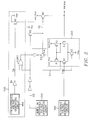
- a reference voltage generating circuit 100 generates a reference voltage Vref.
- a comparator 200 compares an internal source voltage int.Vcc with the reference voltage Vref.
- a driver 90 drives an external source voltage ext.Vcc into the internal source voltage int.Vcc under the control of the comparator 200.
- a burn-in reference voltage generating circuit 300 generates an output signal G3 to prevent the driver 90 from receiving an output signal G1 of the comparator and to fully turn on the driver 90.
- the signal G3 passes through a pair of inverters, and then through a further inverter to a transmission gate N4, P3.
- the circuit is similar to that of Figure 1.
- an additional circuit portion 500 includes a low reference voltage generating circuit 400 is to generate a control signal to prevent the driver 90 from receiving the output signal G1 from the comparator and to fully turn on the driver 90 when the voltage level of the external source voltage ext.Vcc is lower than the voltage level of the reference voltage Vref.
- the burn-in reference voltage generating circuit 300 generates the output signal G3 at a logic "high” state to turn off transmission gate N4, P3, and to turn on a pull-down transistor N5, so that a signal G2 of a logic "low” state is applied to a gate of the driver 90. Consequently the driver 90 is turned on, so that the external source voltage ext.Vcc is directly applied to the memory elements.
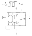
- the low reference voltage generating circuit 400 If the voltage level of the external source voltage ext.Vcc is lower than the voltage level of the reference voltage Vref, the low reference voltage generating circuit 400 generates an output signal of a logic "low” state.
- the output signal of the low reference voltage generator 400 becomes a signal G4 of a logic "high” state by an inverter I4.
- an output signal of a NOR-gate NOR1 has a logic " low “ state, thus turning off the transmission gates N4, P3.
- the signal G4 of a logic "high” state turns on a pull-down transistor N6.
- the voltage level of G2 becomes a ground voltage level Vss, so that the driver 90 is fully turned on so as to apply the external source voltage ext.Vcc to the memory elements of the memory device.
- the transmission gates N4, P3 are turned off to prevent the driver 90 from receiving the output G1 of the comparator 200. This causes the external source voltage ext.Vcc to be stably applied to the memory elements even if the voltage level of the internal source voltage int.Vcc is lower than the voltage level of the reference voltage Vref. Hence the operating speed of the memory device is properly maintained.
- the low reference voltage generating circuit 400 in the circuit for generating the internal source voltage is shown in Figure 3. If a voltage Vref is constant, the sizes of PMOS transistors P14 and P15 with diode characteristics and the value of a resistor R may be adjusted so as to establish a desired voltage level of a node ND1 by a voltage division.
- Comparator 201 comprising NMOS transistor N11, N12, N13 and PMOS transistors P11, P12, compares the voltage level of node ND1 with the voltage Vref, and outputs a corresponding output signal Vout, which controls a PMOS transistor P13 in series with transistors P14, P15.
- the internal source voltage of a predetermined voltage level is applied to the memory elements by the illustrated inventive circuit.
- the external source voltage is directly applied to the memory elements, thus improving the operating speed.
- ground potential (or like terms such as “ground voltage” or “earth” potential or voltage) is used conveniently in this specification to denote a reference potential.
- reference potential may typically be zero potential, it is not essential that it is so, and may be a reference potential other than zero.
Landscapes
- Engineering & Computer Science (AREA)
- Power Engineering (AREA)
- Microelectronics & Electronic Packaging (AREA)
- Computer Hardware Design (AREA)
- Dram (AREA)
- For Increasing The Reliability Of Semiconductor Memories (AREA)
- Static Random-Access Memory (AREA)
- Tests Of Electronic Circuits (AREA)
Applications Claiming Priority (2)
| Application Number | Priority Date | Filing Date | Title |
|---|---|---|---|
| KR1019920005350A KR950008453B1 (ko) | 1992-03-31 | 1992-03-31 | 내부전원전압 발생회로 |
| KR535092 | 1992-03-31 |
Publications (3)
| Publication Number | Publication Date |
|---|---|
| EP0564280A2 true EP0564280A2 (de) | 1993-10-06 |
| EP0564280A3 EP0564280A3 (en) | 1994-08-24 |
| EP0564280B1 EP0564280B1 (de) | 1998-09-16 |
Family
ID=19331163
Family Applications (1)
| Application Number | Title | Priority Date | Filing Date |
|---|---|---|---|
| EP93302561A Expired - Lifetime EP0564280B1 (de) | 1992-03-31 | 1993-03-31 | Schaltung zur Erzeugung einer Innenquellenspannung |
Country Status (8)
| Country | Link |
|---|---|
| US (1) | US5321653A (de) |
| EP (1) | EP0564280B1 (de) |
| JP (1) | JPH06103793A (de) |
| KR (1) | KR950008453B1 (de) |
| CN (1) | CN1043694C (de) |
| DE (1) | DE69321017T2 (de) |
| RU (1) | RU2137178C1 (de) |
| TW (1) | TW217476B (de) |
Cited By (1)
| Publication number | Priority date | Publication date | Assignee | Title |
|---|---|---|---|---|
| DE4434053A1 (de) * | 1993-10-29 | 1995-05-04 | Mitsubishi Electric Corp | Referenzspannungserzeugungsschaltung für Halbleiterspeichervorrichtung |
Families Citing this family (36)
| Publication number | Priority date | Publication date | Assignee | Title |
|---|---|---|---|---|
| KR930008886B1 (ko) * | 1991-08-19 | 1993-09-16 | 삼성전자 주식회사 | 전기적으로 프로그램 할 수 있는 내부전원 발생회로 |
| KR0140673B1 (ko) * | 1993-01-27 | 1998-06-01 | 모리시다 요이찌 | 반도체 메모리 |
| EP0623997B1 (de) * | 1993-05-07 | 1998-08-12 | STMicroelectronics S.r.l. | Mit niedriger Versorgungsspannung arbeitender, eine Hysteresis aufweisender Komparator |
| US5399928A (en) * | 1993-05-28 | 1995-03-21 | Macronix International Co., Ltd. | Negative voltage generator for flash EPROM design |
| US5440519A (en) * | 1994-02-01 | 1995-08-08 | Micron Semiconductor, Inc. | Switched memory expansion buffer |
| JPH07229932A (ja) * | 1994-02-17 | 1995-08-29 | Toshiba Corp | 電位検知回路 |
| US5497348A (en) * | 1994-05-31 | 1996-03-05 | Texas Instruments Incorporated | Burn-in detection circuit |
| US5625305A (en) * | 1994-10-20 | 1997-04-29 | Acer Incorporated | Load detection apparatus |
| JP2785732B2 (ja) * | 1995-02-08 | 1998-08-13 | 日本電気株式会社 | 電源降圧回路 |
| US5570060A (en) * | 1995-03-28 | 1996-10-29 | Sgs-Thomson Microelectronics, Inc. | Circuit for limiting the current in a power transistor |
| JP3629308B2 (ja) * | 1995-08-29 | 2005-03-16 | 株式会社ルネサステクノロジ | 半導体装置およびその試験方法 |
| JP2830799B2 (ja) * | 1995-10-25 | 1998-12-02 | 日本電気株式会社 | 半導体集積回路装置 |
| KR100214466B1 (ko) * | 1995-12-26 | 1999-08-02 | 구본준 | 반도체 메모리의 셀프 번인회로 |
| US5892394A (en) * | 1996-07-19 | 1999-04-06 | Holtek Microelectronics Inc. | Intelligent bias voltage generating circuit |
| JP3516556B2 (ja) * | 1996-08-02 | 2004-04-05 | 沖電気工業株式会社 | 内部電源回路 |
| JP3709246B2 (ja) * | 1996-08-27 | 2005-10-26 | 株式会社日立製作所 | 半導体集積回路 |
| US5838171A (en) * | 1996-11-22 | 1998-11-17 | National Semiconductor Corporation | Low power real-time clock circuit having system and battery power arbitration |
| US5818764A (en) * | 1997-02-06 | 1998-10-06 | Macronix International Co., Ltd. | Block-level wordline enablement to reduce negative wordline stress |
| JP4074697B2 (ja) * | 1997-11-28 | 2008-04-09 | 株式会社ルネサステクノロジ | 半導体装置 |
| US6021083A (en) * | 1997-12-05 | 2000-02-01 | Macronix International Co., Ltd. | Block decoded wordline driver with positive and negative voltage modes |
| JPH11231954A (ja) | 1998-02-16 | 1999-08-27 | Mitsubishi Electric Corp | 内部電源電圧発生回路 |
| KR19990073643A (ko) * | 1998-03-02 | 1999-10-05 | 김영환 | 전원 제어회로 |
| US6023176A (en) * | 1998-03-27 | 2000-02-08 | Cypress Semiconductor Corp. | Input buffer |
| CA2347411C (en) * | 1998-10-21 | 2012-04-03 | The Government Of The United States Of America | Virus-like particles for the induction of autoantibodies |
| JP2000228084A (ja) * | 1999-02-05 | 2000-08-15 | Mitsubishi Electric Corp | 電圧発生回路 |
| KR100323981B1 (ko) * | 1999-09-01 | 2002-02-16 | 윤종용 | 반도체 메모리 장치의 내부전원전압 발생회로 |
| GB2360863B (en) * | 1999-11-15 | 2002-08-28 | Scott C Harris | Automatic cell phone detection at a combustible delivery station |
| KR100550637B1 (ko) * | 2000-12-30 | 2006-02-10 | 주식회사 하이닉스반도체 | 저전압 감지기를 내장한 고전압 검출기 |
| JP4030409B2 (ja) * | 2002-10-31 | 2008-01-09 | 株式会社ルネサステクノロジ | レベル判定回路 |
| JP4393182B2 (ja) * | 2003-05-19 | 2010-01-06 | 三菱電機株式会社 | 電圧発生回路 |
| KR100626367B1 (ko) * | 2003-10-02 | 2006-09-20 | 삼성전자주식회사 | 내부전압 발생장치 |
| US7057447B1 (en) * | 2004-03-04 | 2006-06-06 | National Semiconductor Corporation | Voltage regulator using a single voltage source and method |
| KR100616194B1 (ko) * | 2004-04-20 | 2006-08-25 | 주식회사 하이닉스반도체 | 지연 고정 루프 회로용 내부 전원 전압 발생기 |
| JP4354360B2 (ja) * | 2004-07-26 | 2009-10-28 | Okiセミコンダクタ株式会社 | 降圧電源装置 |
| US9317051B2 (en) * | 2014-02-06 | 2016-04-19 | SK Hynix Inc. | Internal voltage generation circuits |
| JP2016080623A (ja) * | 2014-10-21 | 2016-05-16 | 旭化成エレクトロニクス株式会社 | 半導体集積回路 |
Family Cites Families (10)
| Publication number | Priority date | Publication date | Assignee | Title |
|---|---|---|---|---|
| JP2721151B2 (ja) * | 1986-04-01 | 1998-03-04 | 株式会社東芝 | 半導体集積回路装置 |
| JP2904276B2 (ja) * | 1987-02-24 | 1999-06-14 | 沖電気工業株式会社 | 半導体集積回路装置 |
| US5046052A (en) * | 1988-06-01 | 1991-09-03 | Sony Corporation | Internal low voltage transformation circuit of static random access memory |
| JPH03198296A (ja) * | 1989-12-26 | 1991-08-29 | Nec Corp | 半導体メモリ |
| JP2888898B2 (ja) * | 1990-02-23 | 1999-05-10 | 株式会社日立製作所 | 半導体集積回路 |
| JPH03296118A (ja) * | 1990-04-13 | 1991-12-26 | Oki Micro Design Miyazaki:Kk | 基準電圧発生回路 |
| US5283762A (en) * | 1990-05-09 | 1994-02-01 | Mitsubishi Denki Kabushiki Kaisha | Semiconductor device containing voltage converting circuit and operating method thereof |
| KR930009148B1 (ko) * | 1990-09-29 | 1993-09-23 | 삼성전자 주식회사 | 전원전압 조정회로 |
| JP2945508B2 (ja) * | 1991-06-20 | 1999-09-06 | 三菱電機株式会社 | 半導体装置 |
| KR940008286B1 (ko) * | 1991-08-19 | 1994-09-09 | 삼성전자 주식회사 | 내부전원발생회로 |
-
1992
- 1992-03-31 KR KR1019920005350A patent/KR950008453B1/ko not_active Expired - Fee Related
-
1993
- 1993-03-17 TW TW082101970A patent/TW217476B/zh not_active IP Right Cessation
- 1993-03-24 US US08/035,761 patent/US5321653A/en not_active Expired - Lifetime
- 1993-03-30 RU RU93004646A patent/RU2137178C1/ru not_active IP Right Cessation
- 1993-03-31 DE DE69321017T patent/DE69321017T2/de not_active Expired - Lifetime
- 1993-03-31 EP EP93302561A patent/EP0564280B1/de not_active Expired - Lifetime
- 1993-03-31 CN CN93103554A patent/CN1043694C/zh not_active Expired - Fee Related
- 1993-03-31 JP JP5073697A patent/JPH06103793A/ja active Pending
Cited By (2)
| Publication number | Priority date | Publication date | Assignee | Title |
|---|---|---|---|---|
| DE4434053A1 (de) * | 1993-10-29 | 1995-05-04 | Mitsubishi Electric Corp | Referenzspannungserzeugungsschaltung für Halbleiterspeichervorrichtung |
| US5530397A (en) * | 1993-10-29 | 1996-06-25 | Mitsubishi Denki Kabushiki Kaisha | Reference voltage generating circuit of semiconductor memory device |
Also Published As
| Publication number | Publication date |
|---|---|
| US5321653A (en) | 1994-06-14 |
| DE69321017T2 (de) | 1999-03-04 |
| JPH06103793A (ja) | 1994-04-15 |
| KR930020449A (ko) | 1993-10-19 |
| EP0564280B1 (de) | 1998-09-16 |
| RU2137178C1 (ru) | 1999-09-10 |
| KR950008453B1 (ko) | 1995-07-31 |
| CN1043694C (zh) | 1999-06-16 |
| TW217476B (de) | 1993-12-11 |
| DE69321017D1 (de) | 1998-10-22 |
| CN1077048A (zh) | 1993-10-06 |
| EP0564280A3 (en) | 1994-08-24 |
Similar Documents
| Publication | Publication Date | Title |
|---|---|---|
| EP0564280A2 (de) | Schaltung zur Erzeugung einer Innenquellenspannung | |
| EP0718977B1 (de) | Ausgangssteuerschaltung mit auswählbarem, eingeschränktem Hochspannungsausgang | |
| US5596297A (en) | Output driver circuitry with limited output high voltage | |
| EP0718743B1 (de) | Referenzspannungsquelle mit Verschiebung um eine Schwellenspannung | |
| GB2259575A (en) | Voltage generating circuit | |
| GB2258925A (en) | Power voltage generating circuit | |
| EP0718741B1 (de) | Spannungsregler für einen Ausgangstreiber mit verringerter Ausgangsimpedanz | |
| EP0718744B1 (de) | Einstellbare Stromquelle | |
| US6111457A (en) | Internal power supply circuit for use in a semiconductor device | |
| US5548241A (en) | Voltage reference circuit using an offset compensating current source | |
| EP0718740B1 (de) | Dynamisch gesteuerte Spannungsreferenzschaltung | |
| US6107867A (en) | Load termination sensing circuit | |
| US7525345B2 (en) | Swing limiter | |
| EP0511856A1 (de) | Bezugsgenerator | |
| US6936998B2 (en) | Power glitch free internal voltage generation circuit | |
| US6031395A (en) | CMOS semiconductor circuit for generating high output voltage | |
| US6788586B2 (en) | Output buffer for a nonvolatile memory with output signal switching noise reduction, and nonvolatile memory comprising the same | |
| US6411127B2 (en) | Multi-level bonding option circuit | |
| EP0978726B1 (de) | Halbleitereinrichtung mit einer Prüfschaltung | |
| GB2260661A (en) | Power supply circuit for semiconductor memory device | |
| US6664823B2 (en) | Inverter output circuit | |
| US6023176A (en) | Input buffer | |
| KR100472729B1 (ko) | 데이터 출력버퍼 | |
| KR200210110Y1 (ko) | 오버스트로크방지용 액셀레이터 케이블 | |
| KR100317314B1 (ko) | 커런트모드출력드라이버의전압레벨검출회로 |
Legal Events
| Date | Code | Title | Description |
|---|---|---|---|
| PUAI | Public reference made under article 153(3) epc to a published international application that has entered the european phase |
Free format text: ORIGINAL CODE: 0009012 |
|
| AK | Designated contracting states |
Kind code of ref document: A2 Designated state(s): DE FR GB IT NL |
|
| PUAL | Search report despatched |
Free format text: ORIGINAL CODE: 0009013 |
|
| AK | Designated contracting states |
Kind code of ref document: A3 Designated state(s): DE FR GB IT NL |
|
| 17P | Request for examination filed |
Effective date: 19950224 |
|
| 17Q | First examination report despatched |
Effective date: 19961125 |
|
| GRAG | Despatch of communication of intention to grant |
Free format text: ORIGINAL CODE: EPIDOS AGRA |
|
| GRAG | Despatch of communication of intention to grant |
Free format text: ORIGINAL CODE: EPIDOS AGRA |
|
| GRAH | Despatch of communication of intention to grant a patent |
Free format text: ORIGINAL CODE: EPIDOS IGRA |
|
| GRAH | Despatch of communication of intention to grant a patent |
Free format text: ORIGINAL CODE: EPIDOS IGRA |
|
| GRAA | (expected) grant |
Free format text: ORIGINAL CODE: 0009210 |
|
| AK | Designated contracting states |
Kind code of ref document: B1 Designated state(s): DE FR GB IT NL |
|
| REF | Corresponds to: |
Ref document number: 69321017 Country of ref document: DE Date of ref document: 19981022 |
|
| ET | Fr: translation filed | ||
| PLBE | No opposition filed within time limit |
Free format text: ORIGINAL CODE: 0009261 |
|
| STAA | Information on the status of an ep patent application or granted ep patent |
Free format text: STATUS: NO OPPOSITION FILED WITHIN TIME LIMIT |
|
| 26N | No opposition filed | ||
| REG | Reference to a national code |
Ref country code: GB Ref legal event code: IF02 |
|
| PGFP | Annual fee paid to national office [announced via postgrant information from national office to epo] |
Ref country code: IT Payment date: 20100312 Year of fee payment: 18 |
|
| PGFP | Annual fee paid to national office [announced via postgrant information from national office to epo] |
Ref country code: GB Payment date: 20100226 Year of fee payment: 18 |
|
| PGFP | Annual fee paid to national office [announced via postgrant information from national office to epo] |
Ref country code: FR Payment date: 20100419 Year of fee payment: 18 |
|
| PGFP | Annual fee paid to national office [announced via postgrant information from national office to epo] |
Ref country code: NL Payment date: 20100224 Year of fee payment: 18 Ref country code: DE Payment date: 20100302 Year of fee payment: 18 |
|
| REG | Reference to a national code |
Ref country code: NL Ref legal event code: V1 Effective date: 20111001 |
|
| GBPC | Gb: european patent ceased through non-payment of renewal fee |
Effective date: 20110331 |
|
| REG | Reference to a national code |
Ref country code: FR Ref legal event code: ST Effective date: 20111130 |
|
| PG25 | Lapsed in a contracting state [announced via postgrant information from national office to epo] |
Ref country code: FR Free format text: LAPSE BECAUSE OF NON-PAYMENT OF DUE FEES Effective date: 20110331 Ref country code: NL Free format text: LAPSE BECAUSE OF NON-PAYMENT OF DUE FEES Effective date: 20111001 Ref country code: DE Free format text: LAPSE BECAUSE OF NON-PAYMENT OF DUE FEES Effective date: 20111001 |
|
| REG | Reference to a national code |
Ref country code: DE Ref legal event code: R119 Ref document number: 69321017 Country of ref document: DE Effective date: 20111001 |
|
| PG25 | Lapsed in a contracting state [announced via postgrant information from national office to epo] |
Ref country code: IT Free format text: LAPSE BECAUSE OF NON-PAYMENT OF DUE FEES Effective date: 20110331 Ref country code: GB Free format text: LAPSE BECAUSE OF NON-PAYMENT OF DUE FEES Effective date: 20110331 |