EP0532019B1 - Dispositif semi-conducteur émetteur d'électrons - Google Patents
Dispositif semi-conducteur émetteur d'électrons Download PDFInfo
- Publication number
- EP0532019B1 EP0532019B1 EP92115564A EP92115564A EP0532019B1 EP 0532019 B1 EP0532019 B1 EP 0532019B1 EP 92115564 A EP92115564 A EP 92115564A EP 92115564 A EP92115564 A EP 92115564A EP 0532019 B1 EP0532019 B1 EP 0532019B1
- Authority
- EP
- European Patent Office
- Prior art keywords
- type semiconductor
- concentration
- semiconductor region
- electron emission
- region
- Prior art date
- Legal status (The legal status is an assumption and is not a legal conclusion. Google has not performed a legal analysis and makes no representation as to the accuracy of the status listed.)
- Expired - Lifetime
Links
Images


Classifications
-
- H—ELECTRICITY
- H01—ELECTRIC ELEMENTS
- H01J—ELECTRIC DISCHARGE TUBES OR DISCHARGE LAMPS
- H01J9/00—Apparatus or processes specially adapted for the manufacture, installation, removal, maintenance of electric discharge tubes, discharge lamps, or parts thereof; Recovery of material from discharge tubes or lamps
- H01J9/02—Manufacture of electrodes or electrode systems
- H01J9/022—Manufacture of electrodes or electrode systems of cold cathodes
-
- H—ELECTRICITY
- H01—ELECTRIC ELEMENTS
- H01J—ELECTRIC DISCHARGE TUBES OR DISCHARGE LAMPS
- H01J1/00—Details of electrodes, of magnetic control means, of screens, or of the mounting or spacing thereof, common to two or more basic types of discharge tubes or lamps
- H01J1/02—Main electrodes
- H01J1/30—Cold cathodes, e.g. field-emissive cathode
- H01J1/308—Semiconductor cathodes, e.g. cathodes with PN junction layers
Landscapes
- Engineering & Computer Science (AREA)
- Manufacturing & Machinery (AREA)
- Cold Cathode And The Manufacture (AREA)
Claims (6)
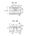
- Dispositif semiconducteur d'émission d'électrons destiné à provoquer un claquage par avalanche en appliquant une tension de polarisation inverse à une jonction à barrière de Schottky entre un film métallique (107 ; 808 ; 1108) et une première région (103 ; 803 ; 1103) en semiconducteur du type p, émettant ainsi extérieurement des électrons (e) à partir d'une surface à l'état solide, dans lequelun substrat (101 ; 801 ; 1101) en semiconducteur du type p est prévu sur une première électrode (106 ; 806, 1106) de contact,une deuxième électrode (108 ; 807 ; 1107) de contact est connectée électriquement audit film métallique (107 ; 808 ; 1108), etune deuxième région (104 ; 804 ; 1104) en semiconducteur de type p destinée à fournir des porteurs à ladite première région (103 ; 803 ; 1103) en semiconducteur du type p est située entre ledit substrat (101 ; 801 ; 1101) en semiconducteur du type p et ladite première région (103 ; 803 ; 1103) en semiconducteur de type p,ledit dispositif semiconducteur d'émission d'électrons étant caractérisé en ce queune troisième région (102 ; 802 ; 1102) en semiconducteur est située sur ledit premier substrat (101 ; 801 ; 1101) en semiconducteur de type p et est formée autour desdites première et deuxième régions (103 ; 803 ; 1103 et 104 ; 804 ; 1104) en semiconducteur de type p.
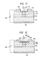
- Dispositif semiconducteur d'émission d'électrons destiné à provoquer un claquage par avalanche en appliquant une tension de polarisation inverse à une jonction pn entre une région (509 ; 905 ; 1205) en semiconducteur du type n et une première région (503 ; 903 ; 1203) en semiconducteur de type p, émettant ainsi extérieurement des électrons (e) à partir d'une surface à l'état solide, dans lequelun substrat (501 ; 901 ; 1201) en semiconducteur du type p est situé sur une première électrode (506 ; 907 ; 1207) de contact,une deuxième électrode (508 ; 908 ; 1208) de contact est connectée électriquement à ladite région (509 ; 907 ; 1207) en semiconducteur du type n, etune deuxième région (504 ; 904 ; 1204) en semiconducteur du type p, destinée à fournir des porteurs à ladite première région (503 ; 903 ; 1203) en semiconducteur du type p, est située entre ledit substrat (501 ; 901 ; 1201) en semiconducteur de type p et ladite première région (503 ; 903 ; 1203) en semiconducteur p, ledit dispositif semi-conducteur d'émission d'électrons étant caractérisé en ce queune troisième région (502 ; 902 ; 1202) en semiconducteur est située sur ledit substrat (501 ; 901 ; 1201) en semiconducteur de type p et est formée autour desdites première et deuxième régions (503 ; 903 ; 1203 et 504 ; 904 ; 1204) en semiconducteur du type p.
- Dispositif selon la revendication 1 ou 2, caractérisé en ce que ladite troisième région en semiconducteur est une région semi-isolante (102 ; 502).
- Dispositif selon la revendication 1 ou 2, caractérisé en ce que ladite troisième région en semiconducteur est une couche (802 ; 902) de semiconducteur de type p à faible concentration.
- Dispositif selon la revendication 1 ou 2, caractérisé en ce que ladite troisième région en semiconducteur est une couche (1102 ; 1202) en semiconducteur de type n à faible concentration.
- Dispositif selon la revendication 2, caractérisé en ce que le dispositif comporte un film de revêtement (507 ; 509 ; 1209) à faible travail d'extraction sur ladite région (509 ; 907 ; 1207) en semiconducteur du type n.
Applications Claiming Priority (4)
| Application Number | Priority Date | Filing Date | Title |
|---|---|---|---|
| JP23469291A JPH0574332A (ja) | 1991-09-13 | 1991-09-13 | 半導体電子放出素子 |
| JP234692/91 | 1991-09-13 | ||
| JP234455/91 | 1991-09-13 | ||
| JP23445591A JPH0574329A (ja) | 1991-09-13 | 1991-09-13 | 半導体電子放出素子 |
Publications (2)
| Publication Number | Publication Date |
|---|---|
| EP0532019A1 EP0532019A1 (fr) | 1993-03-17 |
| EP0532019B1 true EP0532019B1 (fr) | 1997-12-29 |
Family
ID=26531579
Family Applications (1)
| Application Number | Title | Priority Date | Filing Date |
|---|---|---|---|
| EP92115564A Expired - Lifetime EP0532019B1 (fr) | 1991-09-13 | 1992-09-11 | Dispositif semi-conducteur émetteur d'électrons |
Country Status (3)
| Country | Link |
|---|---|
| US (1) | US5760417A (fr) |
| EP (1) | EP0532019B1 (fr) |
| DE (1) | DE69223707T2 (fr) |
Families Citing this family (18)
| Publication number | Priority date | Publication date | Assignee | Title |
|---|---|---|---|---|
| GB9616265D0 (en) * | 1996-08-02 | 1996-09-11 | Philips Electronics Uk Ltd | Electron devices |
| GB9702348D0 (en) * | 1997-02-05 | 1997-03-26 | Smiths Industries Plc | Electron emitter devices |
| US6366266B1 (en) | 1999-09-02 | 2002-04-02 | Micron Technology, Inc. | Method and apparatus for programmable field emission display |
| US6753544B2 (en) * | 2001-04-30 | 2004-06-22 | Hewlett-Packard Development Company, L.P. | Silicon-based dielectric tunneling emitter |
| US6781146B2 (en) | 2001-04-30 | 2004-08-24 | Hewlett-Packard Development Company, L.P. | Annealed tunneling emitter |
| US6911768B2 (en) * | 2001-04-30 | 2005-06-28 | Hewlett-Packard Development Company, L.P. | Tunneling emitter with nanohole openings |
| US6882100B2 (en) * | 2001-04-30 | 2005-04-19 | Hewlett-Packard Development Company, L.P. | Dielectric light device |
| US6558968B1 (en) | 2001-10-31 | 2003-05-06 | Hewlett-Packard Development Company | Method of making an emitter with variable density photoresist layer |
| US6835947B2 (en) * | 2002-01-31 | 2004-12-28 | Hewlett-Packard Development Company, L.P. | Emitter and method of making |
| US6703252B2 (en) * | 2002-01-31 | 2004-03-09 | Hewlett-Packard Development Company, L.P. | Method of manufacturing an emitter |
| US6852554B2 (en) * | 2002-02-27 | 2005-02-08 | Hewlett-Packard Development Company, L.P. | Emission layer formed by rapid thermal formation process |
| US6787792B2 (en) * | 2002-04-18 | 2004-09-07 | Hewlett-Packard Development Company, L.P. | Emitter with filled zeolite emission layer |
| US7170223B2 (en) | 2002-07-17 | 2007-01-30 | Hewlett-Packard Development Company, L.P. | Emitter with dielectric layer having implanted conducting centers |
| US6841794B2 (en) * | 2003-02-18 | 2005-01-11 | Hewlett-Packard Development Company, L.P. | Dielectric emitter with PN junction |
| US7928561B2 (en) * | 2005-09-09 | 2011-04-19 | General Electric Company | Device for thermal transfer and power generation |
| CA2713070C (fr) * | 2008-02-01 | 2016-07-26 | Insiava (Pty) Limited | Dispositif electroluminescent a semi-conducteur comprenant une heterojonction |
| KR20110042188A (ko) * | 2008-10-24 | 2011-04-25 | 가부시키가이샤 어드밴티스트 | 전자 디바이스 및 제조 방법 |
| CN112038455B (zh) * | 2020-08-27 | 2021-12-31 | 厦门士兰明镓化合物半导体有限公司 | 紫外发光二极管及其制造方法 |
Family Cites Families (9)
| Publication number | Priority date | Publication date | Assignee | Title |
|---|---|---|---|---|
| NL184549C (nl) * | 1978-01-27 | 1989-08-16 | Philips Nv | Halfgeleiderinrichting voor het opwekken van een elektronenstroom en weergeefinrichting voorzien van een dergelijke halfgeleiderinrichting. |
| NL184589C (nl) * | 1979-07-13 | 1989-09-01 | Philips Nv | Halfgeleiderinrichting voor het opwekken van een elektronenbundel en werkwijze voor het vervaardigen van een dergelijke halfgeleiderinrichting. |
| US4994708A (en) * | 1986-07-01 | 1991-02-19 | Canon Kabushiki Kaisha | Cold cathode device |
| JP2788243B2 (ja) * | 1988-02-27 | 1998-08-20 | キヤノン株式会社 | 半導体電子放出素子及び半導体電子放出装置 |
| US5107311A (en) * | 1989-08-02 | 1992-04-21 | Canon Kabushiki Kaisha | Semiconductor light-emitting device |
| EP0416558B1 (fr) * | 1989-09-04 | 1996-07-31 | Canon Kabushiki Kaisha | Elément émetteur d'électrons et procédé de fabrication d'un tel élément |
| US5285079A (en) * | 1990-03-16 | 1994-02-08 | Canon Kabushiki Kaisha | Electron emitting device, electron emitting apparatus and electron beam drawing apparatus |
| US5202571A (en) * | 1990-07-06 | 1993-04-13 | Canon Kabushiki Kaisha | Electron emitting device with diamond |
| JPH0512988A (ja) * | 1990-10-13 | 1993-01-22 | Canon Inc | 半導体電子放出素子 |
-
1992
- 1992-09-11 EP EP92115564A patent/EP0532019B1/fr not_active Expired - Lifetime
- 1992-09-11 DE DE69223707T patent/DE69223707T2/de not_active Expired - Fee Related
-
1995
- 1995-03-27 US US08/410,396 patent/US5760417A/en not_active Expired - Fee Related
Also Published As
| Publication number | Publication date |
|---|---|
| US5760417A (en) | 1998-06-02 |
| DE69223707D1 (de) | 1998-02-05 |
| EP0532019A1 (fr) | 1993-03-17 |
| DE69223707T2 (de) | 1998-05-20 |
Similar Documents
| Publication | Publication Date | Title |
|---|---|---|
| EP0532019B1 (fr) | Dispositif semi-conducteur émetteur d'électrons | |
| US5160492A (en) | Buried isolation using ion implantation and subsequent epitaxial growth | |
| US5138402A (en) | Semiconductor electron emitting device | |
| EP0713237B1 (fr) | Elément émetteur d'électrons et son procédé de fabrication | |
| US5414272A (en) | Semiconductor electron emission element | |
| EP1383152A2 (fr) | Emetteur avec couche dielectrique comprenant des centres conducteurs implantes | |
| EP0411612B1 (fr) | Dispositif émetteur de lumière à semi-conducteur | |
| US6577058B2 (en) | Injection cold emitter with negative electron affinity based on wide-gap semiconductor structure with controlling base | |
| KR100189037B1 (ko) | 전계 방출 냉음극 및 그 제조방법 | |
| Miyauchi et al. | Maskless ion implantation technology for III–V compound semiconductors | |
| EP0504603B1 (fr) | Dispositif semiconducteur émetteur d'électrons | |
| JPH0574329A (ja) | 半導体電子放出素子 | |
| US5233196A (en) | Electron beam apparatus and method for driving the same | |
| JP3135070B2 (ja) | 半導体電子放出素子 | |
| JPH06162918A (ja) | 半導体電子放出素子並びにその製造方法 | |
| JPH0574328A (ja) | 半導体電子放出素子 | |
| JP3137267B2 (ja) | 半導体電子放出素子 | |
| JPH0574331A (ja) | 半導体電子放出素子 | |
| JPH0689657A (ja) | 半導体電子放出素子の製造方法 | |
| JP2774155B2 (ja) | 電子放出素子 | |
| JPH0574332A (ja) | 半導体電子放出素子 | |
| JP2780819B2 (ja) | 半導体電子放出素子 | |
| JPH0574330A (ja) | 半導体電子放出素子 | |
| JP2726116B2 (ja) | 半導体電子放出素子およびその製造方法 | |
| JP2820450B2 (ja) | 半導体電子放出素子 |
Legal Events
| Date | Code | Title | Description |
|---|---|---|---|
| PUAI | Public reference made under article 153(3) epc to a published international application that has entered the european phase |
Free format text: ORIGINAL CODE: 0009012 |
|
| AK | Designated contracting states |
Kind code of ref document: A1 Designated state(s): DE FR GB IT NL |
|
| 17P | Request for examination filed |
Effective date: 19930730 |
|
| 17Q | First examination report despatched |
Effective date: 19931207 |
|
| GRAG | Despatch of communication of intention to grant |
Free format text: ORIGINAL CODE: EPIDOS AGRA |
|
| GRAG | Despatch of communication of intention to grant |
Free format text: ORIGINAL CODE: EPIDOS AGRA |
|
| GRAG | Despatch of communication of intention to grant |
Free format text: ORIGINAL CODE: EPIDOS AGRA |
|
| GRAG | Despatch of communication of intention to grant |
Free format text: ORIGINAL CODE: EPIDOS AGRA |
|
| GRAH | Despatch of communication of intention to grant a patent |
Free format text: ORIGINAL CODE: EPIDOS IGRA |
|
| GRAH | Despatch of communication of intention to grant a patent |
Free format text: ORIGINAL CODE: EPIDOS IGRA |
|
| GRAA | (expected) grant |
Free format text: ORIGINAL CODE: 0009210 |
|
| AK | Designated contracting states |
Kind code of ref document: B1 Designated state(s): DE FR GB IT NL |
|
| REF | Corresponds to: |
Ref document number: 69223707 Country of ref document: DE Date of ref document: 19980205 |
|
| ET | Fr: translation filed | ||
| ITF | It: translation for a ep patent filed |
Owner name: SOCIETA' ITALIANA BREVETTI S.P.A. |
|
| PLBE | No opposition filed within time limit |
Free format text: ORIGINAL CODE: 0009261 |
|
| STAA | Information on the status of an ep patent application or granted ep patent |
Free format text: STATUS: NO OPPOSITION FILED WITHIN TIME LIMIT |
|
| 26N | No opposition filed | ||
| REG | Reference to a national code |
Ref country code: GB Ref legal event code: IF02 |
|
| PGFP | Annual fee paid to national office [announced via postgrant information from national office to epo] |
Ref country code: FR Payment date: 20050823 Year of fee payment: 14 |
|
| PGFP | Annual fee paid to national office [announced via postgrant information from national office to epo] |
Ref country code: GB Payment date: 20050907 Year of fee payment: 14 |
|
| PGFP | Annual fee paid to national office [announced via postgrant information from national office to epo] |
Ref country code: DE Payment date: 20050909 Year of fee payment: 14 |
|
| PGFP | Annual fee paid to national office [announced via postgrant information from national office to epo] |
Ref country code: NL Payment date: 20050915 Year of fee payment: 14 |
|
| PGFP | Annual fee paid to national office [announced via postgrant information from national office to epo] |
Ref country code: IT Payment date: 20060930 Year of fee payment: 15 |
|
| PG25 | Lapsed in a contracting state [announced via postgrant information from national office to epo] |
Ref country code: NL Free format text: LAPSE BECAUSE OF NON-PAYMENT OF DUE FEES Effective date: 20070401 |
|
| PG25 | Lapsed in a contracting state [announced via postgrant information from national office to epo] |
Ref country code: DE Free format text: LAPSE BECAUSE OF NON-PAYMENT OF DUE FEES Effective date: 20070403 |
|
| GBPC | Gb: european patent ceased through non-payment of renewal fee |
Effective date: 20060911 |
|
| NLV4 | Nl: lapsed or anulled due to non-payment of the annual fee |
Effective date: 20070401 |
|
| REG | Reference to a national code |
Ref country code: FR Ref legal event code: ST Effective date: 20070531 |
|
| PG25 | Lapsed in a contracting state [announced via postgrant information from national office to epo] |
Ref country code: GB Free format text: LAPSE BECAUSE OF NON-PAYMENT OF DUE FEES Effective date: 20060911 |
|
| PG25 | Lapsed in a contracting state [announced via postgrant information from national office to epo] |
Ref country code: FR Free format text: LAPSE BECAUSE OF NON-PAYMENT OF DUE FEES Effective date: 20061002 |
|
| PG25 | Lapsed in a contracting state [announced via postgrant information from national office to epo] |
Ref country code: IT Free format text: LAPSE BECAUSE OF NON-PAYMENT OF DUE FEES Effective date: 20070911 |