EP0532019B1 - Halbleiter-Elektronenemittierende Einrichtung - Google Patents
Halbleiter-Elektronenemittierende Einrichtung Download PDFInfo
- Publication number
- EP0532019B1 EP0532019B1 EP92115564A EP92115564A EP0532019B1 EP 0532019 B1 EP0532019 B1 EP 0532019B1 EP 92115564 A EP92115564 A EP 92115564A EP 92115564 A EP92115564 A EP 92115564A EP 0532019 B1 EP0532019 B1 EP 0532019B1
- Authority
- EP
- European Patent Office
- Prior art keywords
- type semiconductor
- concentration
- semiconductor region
- electron emission
- region
- Prior art date
- Legal status (The legal status is an assumption and is not a legal conclusion. Google has not performed a legal analysis and makes no representation as to the accuracy of the status listed.)
- Expired - Lifetime
Links
Images


Classifications
-
- H—ELECTRICITY
- H01—ELECTRIC ELEMENTS
- H01J—ELECTRIC DISCHARGE TUBES OR DISCHARGE LAMPS
- H01J9/00—Apparatus or processes specially adapted for the manufacture, installation, removal, maintenance of electric discharge tubes, discharge lamps, or parts thereof; Recovery of material from discharge tubes or lamps
- H01J9/02—Manufacture of electrodes or electrode systems
- H01J9/022—Manufacture of electrodes or electrode systems of cold cathodes
-
- H—ELECTRICITY
- H01—ELECTRIC ELEMENTS
- H01J—ELECTRIC DISCHARGE TUBES OR DISCHARGE LAMPS
- H01J1/00—Details of electrodes, of magnetic control means, of screens, or of the mounting or spacing thereof, common to two or more basic types of discharge tubes or lamps
- H01J1/02—Main electrodes
- H01J1/30—Cold cathodes, e.g. field-emissive cathode
- H01J1/308—Semiconductor cathodes, e.g. cathodes with PN junction layers
Definitions
- the present invention relates to a semiconductor electron emission device and, more particularly, to a semiconductor device for causing an avalanche breakdown so as to emit thermoelectrons.
- the devices described in, e.g., U.S. Patent Nos. 4,259,678 and 4,303,930 are known as ones using an avalanche breakdown mechanism.
- p- and n-type semiconductor layers are formed on a semiconductor substrate, and a cesium film or the like is deposited on the surface of the n-type semiconductor layer to decrease the work function of the surface, thereby forming an electron emission portion.
- thermoelectrons are emitted from the electron emission portion in a direction perpendicular to the surface of the semiconductor substrate.
- a Schottky barrier junction is formed by a p-type semiconductor and a metal material or a p-type semiconductor and a metallic compound, and a reverse bias voltage is applied across the two ends of the Schottky barrier junction to cause an avalanche breakdown so as to generate thermoelectrons, thereby emitting the electrons from an electron emission portion in a direction perpendicular to the surface of a semiconductor substrate.
- the above-mentioned semiconductor electron emission device causes an avalanche breakdown in a high-concentration p-type semiconductor region where a depletion layer having the smallest width is formed upon application of the reverse bias voltage across the two ends of the pn junction or the Schottky barrier junction, and externally emits electrons having high energy generated there from the solid-state surface.
- the depletion layer around the pn junction or the Schottky barrier junction has a radius of curvature determined by the carrier concentration of the semiconductor and the application voltage. Therefore, at an application voltage lower than that causing an avalanche breakdown in the required high-concentration p-type semiconductor region, a breakdown or current leakage occurs around the depletion layer, thus impairing device characteristics.
- the carrier concentration of the p-type semiconductor around the high-concentration p-type semiconductor region causing an avalanche breakdown may be decreased to increase the radius of curvature of a portion around the depletion layer so as to prevent a breakdown at a low voltage there.
- the electrical resistance between an electrode for supplying carriers and the high-concentration p-type semiconductor region causing the avalanche breakdown is increased, not only the operation voltage of the device is increased, but also the device characteristics are impaired by, e.g., generation of Joule's heat.
- a guard ring structure of a high-concentration n-type semiconductor is formed to be concentrical with the high-concentration p-type semiconductor region.
- the depletion layer is formed contiguously outwardly from the high-concentration p-type semiconductor region to extend over the p-type semiconductor region and the high-concentration n-type semiconductor region so as to increase the outermost radius of curvature, thereby preventing a breakdown or current leakage around the depletion layer.
- a semiconductor electron emission device for causing an avalanche breakdown by applying a reverse bias voltage to a Schottky barrier junction between a metallic film and a first p-type semiconductor region, thereby externally emitting electrons from a solid state surface, wherein a p-type semiconductor substrate is provided on a first contact electrode, a second contact electrode is electrically connected to said metallic film, and a second p-type semiconductor region for supplying carriers to said first p-type semiconductor region is provided between said p-type semiconductor substrate and said first p-type semiconductor region, said semiconductor electron emission device being characterized in that a third semiconductor region is provided on said p-type semiconductor substrate and formed around said first and second p-type semiconductor regions.
- a semiconductor electron emission device for causing an avalanche breakdown by applying a reverse bias voltage to a pn junction between an n-type semiconductor region and a first p-type semiconductor region, thereby externally emitting electrons from a solid state surface, wherein a p-type semiconductor substrate is provided on a first contact electrode, a second contact electrode is electrically connected to said n-type semiconductor region, and a second p-type semiconductor region for supplying carriers to said first p-type semiconductor region is provided between said p-type semiconductor substrate and said first p-type semiconductor region, said semiconductor electron emission device being characterized in that a third semiconductor region is provided on said p-type semiconductor substrate and formed around said first and second p-type semiconductor regions.
- the semiconductor electron emission device having the electron emission portion using the Schottky barrier junction of the metallic film and the p-type semiconductor, or the semiconductor electron emission device having the electron emission portion using the pn junction of the n- and p-type semiconductors has a structure comprising the first p-type semiconductor region for forming the Schottky barrier junction or the pn junction, and causing the avalanche breakdown, the second p-type semiconductor region for supplying carriers to the first p-type semiconductor region, and the semi-insulating region located around the first p-type semiconductor region.
- the series resistance of the device can be selected to be an arbitrary value.
- a high-concentration p-type semiconductor region (first region) causing an avalanche breakdown contacts a p-type semiconductor region (second region) for supplying carriers to the first region, and a p-type semiconductor region (third region) for forming the Schottky barrier junction or the pn junction is formed around the first region.
- the first to third regions are formed to have the following relationship among their carrier concentrations: (first region) > (second region) > (third region)
- a portion having a low breakdown voltage (i.e., having a small radius of curvature) around a depletion layer formed in the first region is protected by a depletion layer having a high breakdown voltage (i.e., having a large radius of curvature) formed in the third region contiguously located around the first region and having a low carrier concentration.
- the carrier supply path to the first region has too high a resistance, and the device characteristics are impaired, as described above.
- the series resistance of the device can be selected to be a proper value. Therefore, an element structure requiring no high-concentration n-type semiconductor guard ring structure, which is inconvenient to achieve a simple manufacturing process and a compact device, can be realized.
- the relationship among the carrier concentrations of the first to third regions may be set to satisfy: (second region) ⁇ (first region) > (third region) the high-concentration n-type semiconductor guard ring structure is not required, as described above.
- the carrier concentration of the second region is set to be equal to or higher than that of the first region, the series resistance of the device can be greatly decreased. Therefore, a product RC of a resistance R and an electrical capacitance C can be decreased, and a semiconductor electron emission device having a high operation speed can be manufactured.
- an n-type semiconductor region having a low carrier concentration is formed around a high-concentration first p-type semiconductor region for causing an avalanche breakdown.
- an operation voltage since a portion around a depletion layer formed in the first p-type semiconductor region is contiguously connected to and protected by a depletion layer formed therearound by a pn junction, neither breakdown nor current leakage occur around the first p-type semiconductor region. Therefore, a device structure requiring no high-concentration n-type semiconductor guard ring structure, which is inconvenient to achieve a simple manufacturing process and a compact device, can be realized.
- the series resistance of the device can be selected to be a proper value. Therefore, the device operation speed can be increased.
- Fig. 1 is a sectional view showing a Schottky barrier junction type semiconductor electron emission device according to the first embodiment of the present invention.
- the semiconductor electron emission device of this embodiment is a Schottky barrier junction type device having the following structure. That is, a cylindrical high-concentration p-type semiconductor region 103 as a first p-type semiconductor region, and a cylindrical p-type semiconductor region 104 as a second p-type semiconductor region for supplying carriers to the high-concentration p-type semiconductor region 103 are arranged at substantially the central portion on a high-concentration p-type semiconductor substrate 101 to be in contact with each other.
- a semi-insulating region 102 is formed outwardly concentrically around the high-concentration p-type semiconductor region 103 and the p-type semiconductor region 104.
- a metallic film 107 for forming a Schottky barrier junction with the high-concentration p-type semiconductor region 103 is formed on the device surface.
- the semiconductor electron emission device of this embodiment comprises an ohmic contact electrode 106 for the high-concentration p-type semiconductor substrate 101 and an electrode wiring layer 108 for the metallic film 107 so as to apply a reverse bias voltage to the Schottky barrier junction.
- the reverse bias voltage is applied from a power supply 109 through the ohmic contact electrode 106 and the metallic film 107.
- the electrode wiring layer 108 contacts the metallic film 107 through an insulating film 105 formed along the surface edge portion of the semi-insulating region 102 so as to prevent short-circuiting with the above-mentioned p-type semiconductor region or the semi-insulating region.
- a bottom E c of the conduction band of the p-type semiconductor has a higher energy level than a vacuum level E VAC of a metallic electrode forming the Schottky barrier, and an avalanche breakdown is generated. Electrons generated by the avalanche breakdown obtain energy higher than the lattice temperature by an electric field in a depletion layer formed at a semiconductor-metallic electrode interface, and are injected from the p-type semiconductor to the metallic electrode forming the Schottky barrier. Some electrons having energy larger than the work function of the metallic electrode surface forming the Schottky barrier junction are emitted into vacuum.
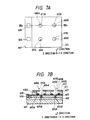
- Fig. 3 shows the shapes of a region 111 where an avalanche breakdown occurs and a depletion region 110 in the Schottky barrier junction type semiconductor electron emission device of this embodiment.
- the semiconductor electron emission device manufactured in this manner was placed in a vacuum chamber maintained at a vacuum of about 1 ⁇ 10 -7 Torr, and a voltage of 7 V was applied from the power supply 109 across the ohmic contact electrode 106 and the electrode wiring layer 108. As a result, electron emission of about 15 pA was observed from the surface of the metallic film 107 on the high-concentration p-type semiconductor region 103.
- the application voltage device voltage
- the electron emission amount emission current
- Fig. 5 shows the electrical characteristics obtained when the semiconductor electron emission device was manufactured while changing only the impurity concentration of the p-type semiconductor region 104 as the second p-type semiconductor region for supplying carriers to the high-concentration p-type semiconductor region 103 as the first p-type semiconductor region to 3 ⁇ 10 18 cm -3 in the above-mentioned manufacturing conditions, and was placed in the same vacuum chamber as described above.
- a device voltage of 5 V was applied from the power supply 109 to this semiconductor electron emission device, electron emission (emission current) of about 20 pA was observed from the surface of the metallic film 107 on the high-concentration p-type semiconductor region 103.
- the emission current was also sequentially increased up to about 100 pA.
- another electrode may be formed on the electrode wiring layer 108 through an insulating film so as to set a potential difference between this electrode and the electrode wiring layer 108.
- the current-voltage characteristics of the semiconductor electron emission device can be regulated.
- the resistance of the p-type semiconductor region 104 is decreased, thereby decreasing the series resistance of the device, and increasing the operation speed.
- GaAs is used as a semiconductor.
- semiconductor materials for example, Si, Ge, GaP, AlAs, GaAsP, AlGaAs, SiC, BP, AlN, diamond, and the like are applicable in principle, and in particular, an indirect transition type material having a wide bandgap is suitable.
- the semi-insulating region 102 can be formed by utilizing various intrinsic crystal defects, a residual impurity, and an intentionally added compensation impurity. When the semi-insulating region 102 is formed, an undoped crystal including no dopant is applicable since it has semi-insulating characteristics.
- the semi-insulating region 102 is formed by implanting B ions.
- B ions When GaAs is used as a semiconductor, various other ion sources such as chromium (Cr), oxygen (O), hydrogen (H), or the like may be used in place of B ions to obtain the same result as described above.
- the material of the ohmic contact electrode 106 in place of tungsten (W), generally known materials such as Al, Au, LaB 6 , and the like may be used as long as they can form a Schottky barrier junction with the p-type semiconductor.
- W tungsten
- the work function of this electrode surface is smaller, the electron emission efficiency is increased.
- a thin film of a material having a low work function such as Cs may be coated on the surface, thereby improving the electron emission efficiency.
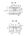
- Figs. 6A and 6B show a pn junction type semiconductor electron emission device according to the second embodiment of the present invention.
- Fig. 6A is a sectional view of the device
- Fig. 6B is a sectional view showing the shape of a depletion layer.
- the semiconductor electron emission device of this embodiment is of a pn junction type device having the following structure. That is, a cylindrical high-concentration p-type semiconductor region 503 as a first p-type semiconductor region and a p-type semiconductor region 504 as a second p-type semiconductor region for supplying carriers to the high-concentration p-type semiconductor region 503 are formed on substantially the central portion on a high-concentration p-type semiconductor substrate 501 to be in contact with each other.
- a semi-insulating region 502 is formed outwardly concentrically around the high-concentration p-type semiconductor region 503 and the p-type semiconductor region 504.
- a high-concentration n-type semiconductor region 509 forming a pn junction with the high-concentration p-type semiconductor region 503 is formed on the device surface.
- the semiconductor electron emission device of this embodiment comprises an ohmic contact electrode 506 for the high-concentration p-type semiconductor substrate 501, an ohmic contact electrode 508 for the high-concentration n-type semiconductor region 509, and a low-work function coating film 507 formed on the surface of the high-concentration n-type semiconductor region 509 so as to apply a reverse bias voltage to the pn junction portion.
- the reverse bias voltage is applied from a power supply 510 through the ohmic contact electrodes 506 and 508.
- the ohmic contact electrode 508 contacts the high-concentration n-type semiconductor region 509 via an insulating film 505 formed along the surface edge portion of the semi-insulating region 502 so as to prevent short-circuiting with the semi-insulating region 502.
- the shape at the edge of a depletion region upon application of the reverse bias voltage is designated by 511, and a region where an avalanche breakdown occurs upon application of the reverse bias voltage is designated by 512.
- the semiconductor electron emission device manufactured in this manner was placed in a vacuum chamber maintained at a vacuum of about 1 ⁇ 10 -11 Torr or less, and a device voltage of 6 V was applied from the power supply 510 across the ohmic contact electrodes 506 and 508. As a result, electron emission of about 0.1 ⁇ A was observed from the surface of the low-work function coating film 507 (Cs) on the high-concentration p-type semiconductor region 503.
- a pn junction type semiconductor electron emission device which has electron emission characteristics equivalent to those of the conventional semiconductor electron emission device, and also has a simple manufacturing process, can be formed.
- another electrode may be formed on the ohmic contact electrode 508 through an insulating film so as to set a potential difference between this electrode and the ohmic contact electrode 508 like in the first embodiment.
- Figs. 7A and 7B show a multi semiconductor electron emission device provided with a plurality of Schottky barrier junction type electron emission portions according to the third embodiment of the present invention.
- Fig. 7A is a plan view of the device, and
- Fig. 7B is a sectional view taken along a line XIIb - XIIb of Fig. 7A.
- four electron emission portions 600A, 600B, 600C, and 600D each having the same structure as that in the first embodiment are arranged in a matrix on a high-concentration p-type semiconductor region 602 formed on a semiconductor substrate 601.
- the electron emission portion 600A Since the electron emission portions 600A, 600B, 600C, and 600D have the same structure, the electron emission portion 600A will be described below.
- the electron emission portion 600A comprises a high-concentration p-type semiconductor region 604A as a first p-type semiconductor region, a p-type semiconductor region 605A as a second p-type semiconductor region, contacting the high-concentration p-type semiconductor region 604A, for supplying carriers to the high-concentration p-type semiconductor region 604A, a semi-insulating region 603 formed around the high-concentration p-type semiconductor region 604A and the p-type semiconductor region 605A, and a Schottky electrode 610A for forming a Schottky barrier junction with the high-concentration p-type semiconductor region 604A.
- an ohmic contact electrode 608 for the high-concentration p-type semiconductor region 602, and an electrode wiring layer 609A for the Schottky electrode 610A are formed so as to apply a reverse bias voltage to the Schottky barrier junction.
- the electrode wiring layer 609A contacts the Schottky electrode 610A on an insulating film 607 formed on the semi-insulating region 603 so as to prevent short-circuiting with the above-mentioned p-type semiconductor region or the semi-insulating region.
- the ohmic contact electrode 608 contacts the high-concentration p-type semiconductor region 602 via a high-concentration p-type semiconductor region 606.
- two electrodes 608 are formed. These ohmic contact electrodes 608 are common to the four electron emission portions 600A, 600B, 600C, and 600D.
- the electrode wiring layer 609A may be commonly connected to electrode wiring layers 609B, 609C, and 609D (609C and 609D are not shown) of the remaining electron emission portions 600B, 600C, and 600D.
- the common ohmic contact electrodes 608 since the common ohmic contact electrodes 608 are used, the electron emission operations of the four electron emission portions 600A, 600B, 600C, and 600D are simultaneously controlled.
- the electrode wiring layers 609A, 609B, 609C, and 609D of the electron emission portions 600A, 600B, 600C, and 600D are independently formed, the electron emission operations can be performed in units of the electron emission portions 600A, 600B, 600C, and 600D.
- the electrode wiring layers may be formed in a matrix, so that electrons are emitted from an electron emission portion corresponding to an intersection where a current flows.
- the device surface formed with the four electron emission portions 600A, 600B, 600C, and 600D with the above-mentioned structure is covered with a gate 612 consisting of a metallic film through a support member 611 formed on the insulating film 607, and formed of an insulating material, except for the ohmic contact electrodes 608. Opening portions 613A, 613B, 613C, and 613D are formed in the gate 612 at corresponding positions above the electron emission portions 600A, 600B, 600C, and 600D.
- Electrons emitted from the electron emission portions 600A, 600B, 600C, and 600D are externally discharged through the opening portions 613A, 613B, 613C, and 613D.
- the pattern of the gate may be arbitrarily changed to be connected to the electrode wiring layers 609A, 609B, 609C, and 609D so as to regulate the flying direction of electrons, or to set a potential difference between the gate and the electrode wiring layers so as to regulate kinetic energy.
- the multi semiconductor electron emission device having the four electron emission portions 600A, 600B, 600C, and 600D was completed.
- a multi semiconductor electron emission device on which 20 (X-direction) ⁇ 10 (Y-direction) electron emission portions were aligned in a matrix was manufactured, was placed in a vacuum chamber maintained at a vacuum of about 1 ⁇ 10 -7 Torr, and a reverse bias voltage of 7 V was applied to all the electron emission portions. As a result, electron emission of a total of about 20 nA was observed. It was confirmed that when a reverse bias voltage was applied across an arbitrary ohmic contact electrode 608 and an arbitrary electrode wiring layer 609, a device at the intersection emitted electrons. In this manner, according to this embodiment, an electron emission device, which has electron emission characteristics equivalent to those of the conventional multi semiconductor electron emission device, and can be easily manufactured, can be formed.
- Fig. 8 is a schematic sectional view showing a semiconductor electron emission device using a Schottky barrier junction according to the fourth embodiment of the present invention.
- the device shown in Fig. 8 comprises a high-concentration p-type semiconductor substrate 801, a low-concentration p-type semiconductor layer 802, a high-concentration p-type semiconductor region (first region) 803 for causing an avalanche breakdown, a p-type semiconductor region (second region) 804 for setting the series resistance of the device, an insulating film 805, an ohmic contact electrode 806 for the p-type semiconductor, an electrode wiring layer 807, a thin metallic film (electrode) 808 for forming a Schottky barrier junction with the p-type semiconductor, and a power supply 809.
- the semiconductor electron emission device (Fig. 8) manufactured in this manner was placed in a vacuum chamber maintained at a vacuum of about 1 ⁇ 10 -7 Torr, and a voltage of 7 V was applied from the power supply 809. As a result, electron emission of about 15 pA from the W surface on the high-concentration p-type semiconductor region 803 was observed. As in Fig. 4, when the application voltage (device voltage) was sequentially increased up to 10 V, the electron emission amount (emission current) was also sequentially increased up to about 100 pA. It is considered that a depletion layer formed upon application of the operation voltage is widened by about 0.04 ⁇ m from the Schottky barrier interface in the high-concentration p-type semiconductor region 803.
- the depletion layer is widened by 0.6 ⁇ m or more, i.e., reaches the high-concentration p-type semiconductor substrate 801 in the low-concentration p-type semiconductor region 802 around the high-concentration p-type semiconductor region 803. Therefore, an electric field is most concentrated on a portion of the high-concentration p-type semiconductor region 803, and an avalanche breakdown efficiently occurs in this region.
- the carrier concentration of the p-type semiconductor region (second region) 804 when the carrier concentration of the p-type semiconductor region (second region) 804 is changed, the current-voltage characteristics of the semiconductor electron emission device can be regulated.
- the resistance of the p-type semiconductor region 804 is decreased, the series resistance of the device can be decreased, and the operation speed can be increased.
- the semiconductor material for example, Si, Ge, GaAs, GaP, AlAs, GaAsP, AlGaAs, SiC, BP, AlN, diamond, and the like are applicable in principle, and in particular, an indirect transition type material having a wide bandgap is suitable.
- the material of the electrode 806, Al, Au, LaB 6 , or the like may be used in place of W as long as the selected material can form a Schottky barrier junction with the p-type semiconductor.
- the work function of this electrode surface is smaller, the electron emission efficiency is increased. For this reason, when the work function of the selected electrode material is large, a thin film of a material having a low work function such as Cs may be coated on the surface, thereby improving the electron emission efficiency.
- Fig. 9 is a schematic sectional view showing a semiconductor electron emission device using a pn junction according to the fifth embodiment of the present invention.
- the device shown in Fig. 9 comprises a high-concentration p-type semiconductor substrate 901, a low-concentration p-type semiconductor layer 902, a high-concentration p-type region semiconductor (first region) 903 for causing an avalanche breakdown, a p-type semiconductor region (second region) 904 for setting the series resistance of the device, a thin high-concentration n-type semiconductor layer 905, an insulating film 906, an ohmic contact electrode 907 for the p-type semiconductor, an ohmic contact electrode 908 for the n-type semiconductor, a coating film 909 of a low-work function material, and a power supply 910.
- the semiconductor electron emission device (Fig. 9) manufactured in this manner was placed in a vacuum chamber maintained at a vacuum of 1 ⁇ 10 -11 Torr or less, and a voltage of 6 V was applied from the power supply 910 to the device. As a result, electron emission of about 0.1 ⁇ A was observed from the Cs surface on the high-concentration p-type semiconductor region 903.
- a pn junction type semiconductor electron emission device which has electron emission characteristics equivalent to those of the conventional semiconductor electron emission device, and has a very simple structure and an easy manufacturing process, can be formed.
- Figs. 10A and 10B partially show a multi electron emission device on which Schottky barrier junction type semiconductor electron emission devices are aligned in a matrix according to the sixth embodiment of the present invention.
- Fig. 10A is a plan view of the device
- Fig. 10B is a sectional view taken along a line Xb - Xb of Fig. 10A. As shown in Figs.
- the device comprises a semi-insulating semiconductor substrate 1001, a stripe-like high-concentration p-type semiconductor region 1002 elongated in the X-direction, a low-concentration p-type semiconductor region 1003, high-concentration p-type semiconductor regions 1004 for causing an avalanche breakdown, p-type semiconductor regions 1005, high-concentration p-type semiconductor regions 1006, an insulating film 1007, ohmic contact electrodes 1008 for the p-type semiconductor, stripe-like electrode wiring layers 1009 elongated in the Y-direction, Schottky electrodes 1010, support members 1011 formed of an insulating material, and a gate 1012 formed of a metallic film.
- the multi semiconductor electron emission device on which 20 (X-direction) ⁇ 10 (Y-direction) electron emission portions manufactured in this manner were aligned in a matrix was placed in a vacuum chamber maintained at a vacuum of about 1 ⁇ 10 -7 Torr, and a reverse bias voltage of 7 V was applied to the entire multi electron emission device. As a result, electron emission of a total of about 20 nA was observed. It was confirmed that when a voltage was applied across an arbitrary ohmic contact electrode 1008 and an arbitrary electrode wiring layer 1009, only a device at the intersection emitted electrons. In this manner, according to the present invention, a device, which has electron emission characteristics equivalent to those of the conventional multi semiconductor electron emission device, and has a very simple structure and an easy manufacturing process, can be formed.
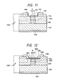
- Fig. 11 is a sectional view showing a Schottky barrier junction type semiconductor electron emission device according to the seventh embodiment of the present invention.
- the semiconductor electron emission device of this embodiment is a Schottky barrier junction type device having the following structure. That is, a cylindrical high-concentration p-type semiconductor region 1103 as a first p-type semiconductor region and a p-type semiconductor region 1104 as a second p-type semiconductor region for supplying carriers to the high-concentration p-type semiconductor region 1103 are formed at substantially the central portion on a high-concentration p-type semiconductor substrate 1101 to be in contact with each other.
- a low-concentration n-type semiconductor region 1102 as an n-type semiconductor region is formed outwardly concentrically around the high-concentration p-type semiconductor region 1103 and the p-type semiconductor region 1104.
- a Schottky electrode 1108 as a metallic film for forming a Schottky barrier junction with the high-concentration p-type semiconductor region 1103 is formed on the device surface.
- the semiconductor electron emission device of this embodiment comprises an ohmic contact electrode 1106 for the high-concentration p-type semiconductor substrate 1101, and an electrode wiring layer 1107 for the Schottky electrode 1108 so as to apply a reverse bias voltage to the Schottky barrier junction.
- the reverse bias voltage is applied from a power supply 1109.
- the electrode wiring layer 1107 contacts the Schottky electrode 1108 on an insulating film 1105 formed on the low-concentration n-type semiconductor region 1102 so as to prevent short-circuiting with the above-mentioned p-type semiconductor regions.
- the shape of a depletion layer edge in a state wherein the reverse bias voltage is applied is designated by 1110.
- the semiconductor electron emission device manufactured in this manner was placed in a vacuum chamber maintained at a vacuum of about 1 ⁇ 10 -7 Torr, and a voltage of 7 V was applied from the power supply 1109 across the ohmic contact electrode 1106 and the electrode wiring layer 1107. As a result, electron emission of about 15 pA was observed from the surface of the Schottky electrode 1108 on the high-concentration p-type semiconductor region 1103.
- the application voltage device voltage
- the electron emission amount emission current
- the depletion layer 1110 upon application of the device voltage is widened by about 0.04 ⁇ m from the Schottky barrier interface with the Schottky electrode 1108 in the high-concentration p-type semiconductor region 1103. Since a portion around the high-concentration p-type semiconductor region 1103 is protected by the thick depletion layer formed by a pn junction, an electric field is most concentrated on a portion of the high-concentration p-type semiconductor region 1103, and an avalanche breakdown efficiently occurs in this region.
- a device voltage of 5 V was applied from the power supply 1109 to this semiconductor electron emission device, electron emission (emission current) of about 20 pA was observed from the surface of the Schottky electrode 1108 on the high-concentration p-type semiconductor region 1103.
- the emission current was also sequentially increased up to about 100 pA.
- another electrode may be formed on the electrode wiring layer 1107 through an insulating film so as to set a potential difference between this electrode and the electrode wiring layer 1107.
- the current-voltage characteristics of the semiconductor electron emission device can be regulated.
- the resistance of the p-type semiconductor region 1104 is decreased, the series resistance of the device can be decreased, and the operation speed can be increased.
- GaAs is used as a semiconductor.
- semiconductor materials for example, Si, Ge, GaP, AlAs, GaAsP, AlGaAs, SiC, BP, AlN, diamond, and the like are applicable in principle, and in particular, an indirect transition type material having a wide bandgap is suitable.
- the material of the ohmic contact electrode 106 in place of tungsten (W), Al, Au, LaB 6 , and the like may be used as long as they can form a Schottky barrier junction with the p-type semiconductor.
- W tungsten
- Al, Au, LaB 6 , and the like may be used as long as they can form a Schottky barrier junction with the p-type semiconductor.
- the work function of this electrode surface is smaller, the electron emission efficiency is increased.
- a thin film of a material having a low work function such as Cs may be coated on the surface, thereby improving the electron emission efficiency.
- Fig. 12 is a sectional view showing a pn junction type semiconductor electron emission device according to the eighth embodiment of the present invention.
- the semiconductor electron emission device of this embodiment is a pn junction type device comprising an electron emission portion having the following structure. That is, in the electron emission portion, a cylindrical high-concentration p-type semiconductor region 1203 as a first p-type semiconductor region, and a p-type semiconductor region 1204 as a second p-type semiconductor region for supplying carriers to the high-concentration p-type semiconductor region 1203 are formed at substantially the central portion on a high-concentration p-type semiconductor substrate 1201 to be in contact with each other.
- a low-concentration n-type semiconductor region 1202 as a second n-type semiconductor region is arranged outwardly concentrically around the high-concentration p-type semiconductor region 1203 and the p-type semiconductor region 1204.
- a high-concentration n-type semiconductor region 1205 as a first n-type semiconductor region for forming a pn junction with the high-concentration p-type semiconductor region 1203 is formed on the high-concentration p-type semiconductor region 1203.
- the semiconductor electron emission device of this embodiment comprises an ohmic contact electrode 1207 for the high-concentration p-type semiconductor substrate 1201, an ohmic contact electrode 1208 for the high-concentration n-type semiconductor region 1205, and a low-work function coating film 1209 formed on the surface of the high-concentration n-type semiconductor region 1205 so as to apply a reverse bias voltage to the pn junction portion.
- the reverse bias voltage is applied from a power supply 1210.
- the ohmic contact electrode 1208 contacts the high-concentration n-type semiconductor region 1205 through an insulating film 1206 formed along the surface edge portion of the low-concentration n-type semiconductor region 1202 so as to prevent short-circuiting with the low-concentration n-type semiconductor region 1202.
- the shape of a depletion layer edge in a state wherein the reverse bias voltage is applied is designated by 1211.
- the semiconductor electron emission device manufactured in this manner was placed in a vacuum chamber maintained at a vacuum of about 1 ⁇ 10 -11 Torr or less, and a device voltage of 6 V was applied from the power supply 1210 across the ohmic contact electrodes 1207 and 1208. As a result, electron emission of about 0.1 ⁇ A was observed from the surface of the low-work function coating film 1209 (Cs) on the high-concentration n-type semiconductor region 1205.
- a pn junction type semiconductor electron emission device which has electron emission characteristics equivalent to those of the conventional semiconductor electron emission device, and has an easy manufacturing process, can be formed.
- the flying direction and kinetic energy of electrons can be regulated like in the seventh embodiment.
- Fig. 13 shows a Schottky barrier type multi semiconductor electron emission device on which a plurality of electron emission portions are formed according to the ninth embodiment of the present invention.
- Fig. 13A is a plan view of the device, and
- Fig. 13B is a sectional view taken along a line XIIIb - XIIIb of Fig. 13A.
- four electron emission portions 1300A, 1300B, 1300C, and 1300D are formed in a matrix on a high-concentration p-type semiconductor region 1302 formed on a semiconductor substrate 1301.
- the electron emission portion 1300A Since the electron emission portions 1300A, 1300B, 1300C, and 1300D have the same structure, the electron emission portion 1300A will be exemplified below.
- the electron emission portion 1300A has the same structure as that of the device of the seventh embodiment. That is, the portion 1300A comprises a high-concentration p-type semiconductor region 1304A as a first p-type semiconductor region, a p-type semiconductor region 1305A as a second p-type semiconductor region, contacting the high-concentration p-type semiconductor region 1304A, for supplying carriers to the high-concentration p-type semiconductor region 1304A, a low-concentration n-type semiconductor region 1303 as an n-type semiconductor region formed around the high-concentration p-type semiconductor region 1304A and the p-type semiconductor region 1305A, and a Schottky electrode 1310A for forming a Schottky barrier junction with the high-concentration p-type semiconductor region 1304A.
- an ohmic contact electrode 1308 for the high-concentration p-type semiconductor region 1302 and an electrode wiring layer 1309A for the Schottky electrode 1310A were formed so as to apply a reverse bias voltage to the Schottky barrier junction.
- the electrode wiring layer 1309A contacts the Schottky electrode 1310A on an insulating film 1307 formed on the low-concentration n-type semiconductor region 1303 so as to prevent short-circuiting with the above-mentioned p-type semiconductor regions.
- the ohmic contact electrode 1308 is connected to the high-concentration p-type semiconductor region 1302 through a high-concentration p-type semiconductor region 1306. In this embodiment, as shown in Fig. 13A, two ohmic contact electrodes 1308 are formed. The ohmic contact electrodes 1308 are common to the four electron emission portions 1300A, 1300B, 1300C, and 1300D.
- the Schottky electrode 1310A may be commonly connected to Schottky electrodes 1310B, 1310C, and 1310D (1310C and 1310D are not shown) of the remaining electron emission portions 1300B, 1300C, and 1300D.
- the ohmic contact electrodes 1308 are commonly connected, the electron emission operations of the four electron emission portions 1300A, 1300B, 1300C, and 1300D are simultaneously controlled.
- the Schottky electrodes 1310A, 1310B, 1310C, and 1310D of the electron emission portions 1300A, 1300B, 1300C, and 1300D are independently formed, the electron emission portions 1300A, 1300B, 1300C, and 1300D can be controlled independently.
- the device surface formed with the four electron emission portions 1300A, 1300B, 1300C, and 1300D with the above-mentioned structure is covered with a gate 1312 consisting of a metallic film through a support member 1311 formed on the insulating film 1307, and formed of an insulating material, except for the ohmic contact electrodes 1308. Opening portions 1313A, 1313B, 1313C, and 1313D are formed in the gate 1312 at corresponding positions above the electron emission portions 1300A, 1300B, 1300C, and 1300D. Electrons emitted from the electron emission portions 1300A, 1300B, 1300C, and 1300D are externally discharged through the opening portions 1313A, 1313B, 1313C, and 1313D.
- the multi semiconductor electron emission device having the four electron emission portions 1300A, 1300B, 1300C, and 1300D was completed.
- a multi semiconductor electron emission device on which 20 (X-direction) ⁇ 10 (Y-direction) electron emission portions were aligned in a matrix was manufactured, was placed in a vacuum chamber maintained at a vacuum of about 1 ⁇ 10 -7 Torr, and a reverse bias voltage of 7 V was applied to all the electron emission portions. As a result, electron emission of a total of about 20 nA was observed. It was confirmed that when a reverse bias voltage was applied across an arbitrary ohmic contact electrode 1308 and an arbitrary electrode wiring layer 1309, a device at the intersection emitted electrons. In this manner, according to this embodiment, an electron emission device, which has electron emission characteristics equivalent to those of the conventional multi semiconductor electron emission device, and can be easily manufactured, can be formed.
- the present invention can provide the following effects.
- the high-concentration p-type semiconductor region (first region) for causing an avalanche breakdown contacts the p-type semiconductor region (second region) for supplying carriers to the first region, and the p-type semiconductor region (third region) for forming a Schottky barrier junction or pn junction is formed around the first region.
- first region for causing an avalanche breakdown contacts the p-type semiconductor region (second region) for supplying carriers to the first region
- the p-type semiconductor region (third region) for forming a Schottky barrier junction or pn junction is formed around the first region.
- the depletion layer can have a shape with which an electric field can be most easily concentrated on the first p-type semiconductor region.
- the series resistance of the device can be decreased. Therefore, a semiconductor electron emission device having a high operation speed can be provided.
Landscapes
- Engineering & Computer Science (AREA)
- Manufacturing & Machinery (AREA)
- Cold Cathode And The Manufacture (AREA)
Claims (6)
- Halbleiter- Elektronenemissionseinrichtung zur Herbeiführung eines Lawinendurchbruchs durch Anlegen einer Vorspannung in Rückwärtsrichtung an eine Schottky- Sperrschicht zwischen einem Metallfilm (107; 808; 1108) und einer ersten p- dotierten Halbleiterzone (103; 803; 1103), wodurch extern emittierte Elektronen (e) aus einer Halbleiteroberfläche emittiert werden, wobeiein p- dotiertes Halbleitersubstrat (101; 801; 1101) vorgesehen ist auf einer ersten Kontaktelektrode (106; 806; 1106), eine zweite Kontaktelektrode (108; 807; 1107) ist elektrisch mit dem Metallfilm (107; 808; 1108) verbunden, und eine zweite p- dotierte Halbleiterzone (104; 804; 1104) zur Lieferung von Ladungsträgern zur ersten p- dotierten Halbleiterzone ist vorgesehen zwischen dem p- dotierten Halbleitersubstrat (101; 801; 1101) und der ersten p- dotierten Halbleiterzone (103; 803; 1103), dadurch gekennzeichnet,daß eine dritte Halbleiterzone (102; 802; 1102) auf dem p-dotierten Halbleitersubstrat (101; 801; 1101) vorgesehen und um die erste und zweite p- dotierte Halbleiterzone (103; 803; 1103 und 104; 804; 1104) gebildet ist.
- Halbleiter- Elektronenemissionseinrichtung zur Herbeiführung eines Lawinendurchbruchs durch Anlegen einer Vorspannung in Rückwärtsrichtung an einen pn- Übergang zwischen einer n-dotierten Halbleiterzone (509; 905; 1205) und einer ersten p-dotierten Halbleiterzone (503; 903; 1203), wodurch Elektronen (e) aus der Halbleiteroberfläche nach außen emittiert werden, wobeiein p- dotiertes Halbleitersubstrat (501; 901; 1201) auf der ersten Kontaktelektrode (506; 907; 1207) vorgesehen ist, eine zweite Kontaktelektrode (508; 908; 1208) elektrisch mit der n-dotierten Halbleiterzone (509; 907; 1207) verbunden ist, undeine zweite p- dotierte Halbleiterzone (504; 904; 1204) zur Lieferung von Ladungsträgern an die erste p- dotierte Halbleiterzone (503; 903; 1203) zwischen dem ersten p- dotierten Halbleitersubstrat (501, 901; 1201) und der erstenp-dotierten Halbleiterzone (503; 903; 1203) vorgesehen ist, dadurch gekennzeichnet,daß eine dritte Halbleiterzone (502; 902; 1202) auf dem p-dotierten Halbleitersubstrat (501; 901; 1201) vorgesehen und um die erste und zweite p- dotierte Halbleiterzone (503; 903; 1203 und 504; 904; 1204) gebildet ist.
- Einrichtung nach Anspruch 1 oder 2, dadurch gekennzeichnet, daß die dritte Halbleiterzone eine halbisolierende Zone (102; 502) ist.
- Einrichtung nach Anspruch 1 oder 2, dadurch gekennzeichnet, daß die dritte Halbleiterzone eine niedrig konzentrierte, p- dotierte Halbleiterschicht (802; 902) ist.
- Einrichtung nach Anspruch 1 oder 2, dadurch gekennzeichnet, daß die dritte Halbleiterzone eine niedrig konzentrierte, n- dotierte Halbleiterschicht (1102; 1202) ist.
- Einrichtung nach Anspruch 2, dadurch gekennzeichnet, daß die Einrichtung des weiteren mit einem Deckfilm (507; 909; 1209) mit niedriger Austrittsarbeit auf der n- dotierten Halbleiterzone (509; 907; 1207) ausgestattet ist.
Applications Claiming Priority (4)
| Application Number | Priority Date | Filing Date | Title |
|---|---|---|---|
| JP23469291A JPH0574332A (ja) | 1991-09-13 | 1991-09-13 | 半導体電子放出素子 |
| JP234455/91 | 1991-09-13 | ||
| JP234692/91 | 1991-09-13 | ||
| JP23445591A JPH0574329A (ja) | 1991-09-13 | 1991-09-13 | 半導体電子放出素子 |
Publications (2)
| Publication Number | Publication Date |
|---|---|
| EP0532019A1 EP0532019A1 (de) | 1993-03-17 |
| EP0532019B1 true EP0532019B1 (de) | 1997-12-29 |
Family
ID=26531579
Family Applications (1)
| Application Number | Title | Priority Date | Filing Date |
|---|---|---|---|
| EP92115564A Expired - Lifetime EP0532019B1 (de) | 1991-09-13 | 1992-09-11 | Halbleiter-Elektronenemittierende Einrichtung |
Country Status (3)
| Country | Link |
|---|---|
| US (1) | US5760417A (de) |
| EP (1) | EP0532019B1 (de) |
| DE (1) | DE69223707T2 (de) |
Families Citing this family (18)
| Publication number | Priority date | Publication date | Assignee | Title |
|---|---|---|---|---|
| GB9616265D0 (en) * | 1996-08-02 | 1996-09-11 | Philips Electronics Uk Ltd | Electron devices |
| GB9702348D0 (en) * | 1997-02-05 | 1997-03-26 | Smiths Industries Plc | Electron emitter devices |
| US6366266B1 (en) | 1999-09-02 | 2002-04-02 | Micron Technology, Inc. | Method and apparatus for programmable field emission display |
| US6911768B2 (en) * | 2001-04-30 | 2005-06-28 | Hewlett-Packard Development Company, L.P. | Tunneling emitter with nanohole openings |
| US6753544B2 (en) * | 2001-04-30 | 2004-06-22 | Hewlett-Packard Development Company, L.P. | Silicon-based dielectric tunneling emitter |
| US6781146B2 (en) | 2001-04-30 | 2004-08-24 | Hewlett-Packard Development Company, L.P. | Annealed tunneling emitter |
| US6882100B2 (en) * | 2001-04-30 | 2005-04-19 | Hewlett-Packard Development Company, L.P. | Dielectric light device |
| US6558968B1 (en) | 2001-10-31 | 2003-05-06 | Hewlett-Packard Development Company | Method of making an emitter with variable density photoresist layer |
| US6703252B2 (en) * | 2002-01-31 | 2004-03-09 | Hewlett-Packard Development Company, L.P. | Method of manufacturing an emitter |
| US6835947B2 (en) * | 2002-01-31 | 2004-12-28 | Hewlett-Packard Development Company, L.P. | Emitter and method of making |
| US6852554B2 (en) * | 2002-02-27 | 2005-02-08 | Hewlett-Packard Development Company, L.P. | Emission layer formed by rapid thermal formation process |
| US6787792B2 (en) * | 2002-04-18 | 2004-09-07 | Hewlett-Packard Development Company, L.P. | Emitter with filled zeolite emission layer |
| US7170223B2 (en) | 2002-07-17 | 2007-01-30 | Hewlett-Packard Development Company, L.P. | Emitter with dielectric layer having implanted conducting centers |
| US6841794B2 (en) * | 2003-02-18 | 2005-01-11 | Hewlett-Packard Development Company, L.P. | Dielectric emitter with PN junction |
| US7928561B2 (en) * | 2005-09-09 | 2011-04-19 | General Electric Company | Device for thermal transfer and power generation |
| WO2009095886A2 (en) * | 2008-02-01 | 2009-08-06 | Insiava (Pty) Limited | Semiconductor light emitting device comprising heterojunction |
| JPWO2010046997A1 (ja) * | 2008-10-24 | 2012-03-15 | 株式会社アドバンテスト | 電子デバイスおよび製造方法 |
| CN112038455B (zh) * | 2020-08-27 | 2021-12-31 | 厦门士兰明镓化合物半导体有限公司 | 紫外发光二极管及其制造方法 |
Family Cites Families (9)
| Publication number | Priority date | Publication date | Assignee | Title |
|---|---|---|---|---|
| NL184549C (nl) * | 1978-01-27 | 1989-08-16 | Philips Nv | Halfgeleiderinrichting voor het opwekken van een elektronenstroom en weergeefinrichting voorzien van een dergelijke halfgeleiderinrichting. |
| NL184589C (nl) * | 1979-07-13 | 1989-09-01 | Philips Nv | Halfgeleiderinrichting voor het opwekken van een elektronenbundel en werkwijze voor het vervaardigen van een dergelijke halfgeleiderinrichting. |
| US4994708A (en) * | 1986-07-01 | 1991-02-19 | Canon Kabushiki Kaisha | Cold cathode device |
| JP2788243B2 (ja) * | 1988-02-27 | 1998-08-20 | キヤノン株式会社 | 半導体電子放出素子及び半導体電子放出装置 |
| US5107311A (en) * | 1989-08-02 | 1992-04-21 | Canon Kabushiki Kaisha | Semiconductor light-emitting device |
| EP0713237B1 (de) * | 1989-09-04 | 2000-12-27 | Canon Kabushiki Kaisha | Elektronenemissionselement- und Herstellungsverfahren desselben |
| US5285079A (en) * | 1990-03-16 | 1994-02-08 | Canon Kabushiki Kaisha | Electron emitting device, electron emitting apparatus and electron beam drawing apparatus |
| US5202571A (en) * | 1990-07-06 | 1993-04-13 | Canon Kabushiki Kaisha | Electron emitting device with diamond |
| JPH0512988A (ja) * | 1990-10-13 | 1993-01-22 | Canon Inc | 半導体電子放出素子 |
-
1992
- 1992-09-11 EP EP92115564A patent/EP0532019B1/de not_active Expired - Lifetime
- 1992-09-11 DE DE69223707T patent/DE69223707T2/de not_active Expired - Fee Related
-
1995
- 1995-03-27 US US08/410,396 patent/US5760417A/en not_active Expired - Fee Related
Also Published As
| Publication number | Publication date |
|---|---|
| EP0532019A1 (de) | 1993-03-17 |
| DE69223707D1 (de) | 1998-02-05 |
| US5760417A (en) | 1998-06-02 |
| DE69223707T2 (de) | 1998-05-20 |
Similar Documents
| Publication | Publication Date | Title |
|---|---|---|
| EP0532019B1 (de) | Halbleiter-Elektronenemittierende Einrichtung | |
| US5160492A (en) | Buried isolation using ion implantation and subsequent epitaxial growth | |
| US5138402A (en) | Semiconductor electron emitting device | |
| EP0713237B1 (de) | Elektronenemissionselement- und Herstellungsverfahren desselben | |
| US5414272A (en) | Semiconductor electron emission element | |
| EP1383152A2 (de) | Emitter mit dielektrischer Schicht mit implantierten leitenden Zentren | |
| EP0411612B1 (de) | Halbleiter lichtemittierende Vorrichtung | |
| US6577058B2 (en) | Injection cold emitter with negative electron affinity based on wide-gap semiconductor structure with controlling base | |
| KR100189037B1 (ko) | 전계 방출 냉음극 및 그 제조방법 | |
| Miyauchi et al. | Maskless ion implantation technology for III–V compound semiconductors | |
| EP0504603B1 (de) | Halbleiter-Elektronenemissionseinrichtung | |
| JPH0574329A (ja) | 半導体電子放出素子 | |
| US5233196A (en) | Electron beam apparatus and method for driving the same | |
| JP3135070B2 (ja) | 半導体電子放出素子 | |
| JPH06162918A (ja) | 半導体電子放出素子並びにその製造方法 | |
| JPH0574328A (ja) | 半導体電子放出素子 | |
| JP3137267B2 (ja) | 半導体電子放出素子 | |
| JPH0574331A (ja) | 半導体電子放出素子 | |
| JPH0689657A (ja) | 半導体電子放出素子の製造方法 | |
| JP2774155B2 (ja) | 電子放出素子 | |
| JPH0574332A (ja) | 半導体電子放出素子 | |
| JP2780819B2 (ja) | 半導体電子放出素子 | |
| JPH0574330A (ja) | 半導体電子放出素子 | |
| JP2726116B2 (ja) | 半導体電子放出素子およびその製造方法 | |
| JP2820450B2 (ja) | 半導体電子放出素子 |
Legal Events
| Date | Code | Title | Description |
|---|---|---|---|
| PUAI | Public reference made under article 153(3) epc to a published international application that has entered the european phase |
Free format text: ORIGINAL CODE: 0009012 |
|
| AK | Designated contracting states |
Kind code of ref document: A1 Designated state(s): DE FR GB IT NL |
|
| 17P | Request for examination filed |
Effective date: 19930730 |
|
| 17Q | First examination report despatched |
Effective date: 19931207 |
|
| GRAG | Despatch of communication of intention to grant |
Free format text: ORIGINAL CODE: EPIDOS AGRA |
|
| GRAG | Despatch of communication of intention to grant |
Free format text: ORIGINAL CODE: EPIDOS AGRA |
|
| GRAG | Despatch of communication of intention to grant |
Free format text: ORIGINAL CODE: EPIDOS AGRA |
|
| GRAG | Despatch of communication of intention to grant |
Free format text: ORIGINAL CODE: EPIDOS AGRA |
|
| GRAH | Despatch of communication of intention to grant a patent |
Free format text: ORIGINAL CODE: EPIDOS IGRA |
|
| GRAH | Despatch of communication of intention to grant a patent |
Free format text: ORIGINAL CODE: EPIDOS IGRA |
|
| GRAA | (expected) grant |
Free format text: ORIGINAL CODE: 0009210 |
|
| AK | Designated contracting states |
Kind code of ref document: B1 Designated state(s): DE FR GB IT NL |
|
| REF | Corresponds to: |
Ref document number: 69223707 Country of ref document: DE Date of ref document: 19980205 |
|
| ET | Fr: translation filed | ||
| ITF | It: translation for a ep patent filed |
Owner name: SOCIETA' ITALIANA BREVETTI S.P.A. |
|
| PLBE | No opposition filed within time limit |
Free format text: ORIGINAL CODE: 0009261 |
|
| STAA | Information on the status of an ep patent application or granted ep patent |
Free format text: STATUS: NO OPPOSITION FILED WITHIN TIME LIMIT |
|
| 26N | No opposition filed | ||
| REG | Reference to a national code |
Ref country code: GB Ref legal event code: IF02 |
|
| PGFP | Annual fee paid to national office [announced via postgrant information from national office to epo] |
Ref country code: FR Payment date: 20050823 Year of fee payment: 14 |
|
| PGFP | Annual fee paid to national office [announced via postgrant information from national office to epo] |
Ref country code: GB Payment date: 20050907 Year of fee payment: 14 |
|
| PGFP | Annual fee paid to national office [announced via postgrant information from national office to epo] |
Ref country code: DE Payment date: 20050909 Year of fee payment: 14 |
|
| PGFP | Annual fee paid to national office [announced via postgrant information from national office to epo] |
Ref country code: NL Payment date: 20050915 Year of fee payment: 14 |
|
| PGFP | Annual fee paid to national office [announced via postgrant information from national office to epo] |
Ref country code: IT Payment date: 20060930 Year of fee payment: 15 |
|
| PG25 | Lapsed in a contracting state [announced via postgrant information from national office to epo] |
Ref country code: NL Free format text: LAPSE BECAUSE OF NON-PAYMENT OF DUE FEES Effective date: 20070401 |
|
| PG25 | Lapsed in a contracting state [announced via postgrant information from national office to epo] |
Ref country code: DE Free format text: LAPSE BECAUSE OF NON-PAYMENT OF DUE FEES Effective date: 20070403 |
|
| GBPC | Gb: european patent ceased through non-payment of renewal fee |
Effective date: 20060911 |
|
| NLV4 | Nl: lapsed or anulled due to non-payment of the annual fee |
Effective date: 20070401 |
|
| REG | Reference to a national code |
Ref country code: FR Ref legal event code: ST Effective date: 20070531 |
|
| PG25 | Lapsed in a contracting state [announced via postgrant information from national office to epo] |
Ref country code: GB Free format text: LAPSE BECAUSE OF NON-PAYMENT OF DUE FEES Effective date: 20060911 |
|
| PG25 | Lapsed in a contracting state [announced via postgrant information from national office to epo] |
Ref country code: FR Free format text: LAPSE BECAUSE OF NON-PAYMENT OF DUE FEES Effective date: 20061002 |
|
| PG25 | Lapsed in a contracting state [announced via postgrant information from national office to epo] |
Ref country code: IT Free format text: LAPSE BECAUSE OF NON-PAYMENT OF DUE FEES Effective date: 20070911 |