EP0504911A2 - Flüssigkristallvorrichtung - Google Patents
Flüssigkristallvorrichtung Download PDFInfo
- Publication number
- EP0504911A2 EP0504911A2 EP92104850A EP92104850A EP0504911A2 EP 0504911 A2 EP0504911 A2 EP 0504911A2 EP 92104850 A EP92104850 A EP 92104850A EP 92104850 A EP92104850 A EP 92104850A EP 0504911 A2 EP0504911 A2 EP 0504911A2
- Authority
- EP
- European Patent Office
- Prior art keywords
- liquid crystal
- pair
- substrates
- injection port
- phase
- Prior art date
- Legal status (The legal status is an assumption and is not a legal conclusion. Google has not performed a legal analysis and makes no representation as to the accuracy of the status listed.)
- Granted
Links
Images


Classifications
-
- G—PHYSICS
- G02—OPTICS
- G02F—OPTICAL DEVICES OR ARRANGEMENTS FOR THE CONTROL OF LIGHT BY MODIFICATION OF THE OPTICAL PROPERTIES OF THE MEDIA OF THE ELEMENTS INVOLVED THEREIN; NON-LINEAR OPTICS; FREQUENCY-CHANGING OF LIGHT; OPTICAL LOGIC ELEMENTS; OPTICAL ANALOGUE/DIGITAL CONVERTERS
- G02F1/00—Devices or arrangements for the control of the intensity, colour, phase, polarisation or direction of light arriving from an independent light source, e.g. switching, gating or modulating; Non-linear optics
- G02F1/01—Devices or arrangements for the control of the intensity, colour, phase, polarisation or direction of light arriving from an independent light source, e.g. switching, gating or modulating; Non-linear optics for the control of the intensity, phase, polarisation or colour
- G02F1/13—Devices or arrangements for the control of the intensity, colour, phase, polarisation or direction of light arriving from an independent light source, e.g. switching, gating or modulating; Non-linear optics for the control of the intensity, phase, polarisation or colour based on liquid crystals, e.g. single liquid crystal display cells
- G02F1/133—Constructional arrangements; Operation of liquid crystal cells; Circuit arrangements
- G02F1/1333—Constructional arrangements; Manufacturing methods
- G02F1/1341—Filling or closing of cells
-
- G—PHYSICS
- G02—OPTICS
- G02F—OPTICAL DEVICES OR ARRANGEMENTS FOR THE CONTROL OF LIGHT BY MODIFICATION OF THE OPTICAL PROPERTIES OF THE MEDIA OF THE ELEMENTS INVOLVED THEREIN; NON-LINEAR OPTICS; FREQUENCY-CHANGING OF LIGHT; OPTICAL LOGIC ELEMENTS; OPTICAL ANALOGUE/DIGITAL CONVERTERS
- G02F1/00—Devices or arrangements for the control of the intensity, colour, phase, polarisation or direction of light arriving from an independent light source, e.g. switching, gating or modulating; Non-linear optics
- G02F1/01—Devices or arrangements for the control of the intensity, colour, phase, polarisation or direction of light arriving from an independent light source, e.g. switching, gating or modulating; Non-linear optics for the control of the intensity, phase, polarisation or colour
- G02F1/13—Devices or arrangements for the control of the intensity, colour, phase, polarisation or direction of light arriving from an independent light source, e.g. switching, gating or modulating; Non-linear optics for the control of the intensity, phase, polarisation or colour based on liquid crystals, e.g. single liquid crystal display cells
- G02F1/133—Constructional arrangements; Operation of liquid crystal cells; Circuit arrangements
- G02F1/1333—Constructional arrangements; Manufacturing methods
- G02F1/1337—Surface-induced orientation of the liquid crystal molecules, e.g. by alignment layers
-
- G—PHYSICS
- G02—OPTICS
- G02F—OPTICAL DEVICES OR ARRANGEMENTS FOR THE CONTROL OF LIGHT BY MODIFICATION OF THE OPTICAL PROPERTIES OF THE MEDIA OF THE ELEMENTS INVOLVED THEREIN; NON-LINEAR OPTICS; FREQUENCY-CHANGING OF LIGHT; OPTICAL LOGIC ELEMENTS; OPTICAL ANALOGUE/DIGITAL CONVERTERS
- G02F1/00—Devices or arrangements for the control of the intensity, colour, phase, polarisation or direction of light arriving from an independent light source, e.g. switching, gating or modulating; Non-linear optics
- G02F1/01—Devices or arrangements for the control of the intensity, colour, phase, polarisation or direction of light arriving from an independent light source, e.g. switching, gating or modulating; Non-linear optics for the control of the intensity, phase, polarisation or colour
- G02F1/13—Devices or arrangements for the control of the intensity, colour, phase, polarisation or direction of light arriving from an independent light source, e.g. switching, gating or modulating; Non-linear optics for the control of the intensity, phase, polarisation or colour based on liquid crystals, e.g. single liquid crystal display cells
- G02F1/137—Devices or arrangements for the control of the intensity, colour, phase, polarisation or direction of light arriving from an independent light source, e.g. switching, gating or modulating; Non-linear optics for the control of the intensity, phase, polarisation or colour based on liquid crystals, e.g. single liquid crystal display cells characterised by the electro-optical or magneto-optical effect, e.g. field-induced phase transition, orientation effect, guest-host interaction or dynamic scattering
- G02F1/139—Devices or arrangements for the control of the intensity, colour, phase, polarisation or direction of light arriving from an independent light source, e.g. switching, gating or modulating; Non-linear optics for the control of the intensity, phase, polarisation or colour based on liquid crystals, e.g. single liquid crystal display cells characterised by the electro-optical or magneto-optical effect, e.g. field-induced phase transition, orientation effect, guest-host interaction or dynamic scattering based on orientation effects in which the liquid crystal remains transparent
- G02F1/141—Devices or arrangements for the control of the intensity, colour, phase, polarisation or direction of light arriving from an independent light source, e.g. switching, gating or modulating; Non-linear optics for the control of the intensity, phase, polarisation or colour based on liquid crystals, e.g. single liquid crystal display cells characterised by the electro-optical or magneto-optical effect, e.g. field-induced phase transition, orientation effect, guest-host interaction or dynamic scattering based on orientation effects in which the liquid crystal remains transparent using ferroelectric liquid crystals
Definitions
- the invention relates to a liquid crystal device using a chiral smectic liquid crystal having ferroelectricity.
- a liquid crystal device having bistability has been proposed by Clark and Lagerwall (specification of U.S.P. No. 4,367,924 and the like).
- a liquid crystal having bistability a ferroelectric liquid crystal having a chiral smectic C phase (SmC*) or H phase (SmH*) is generally used.
- the above liquid crystal has a bistable state comprising first and second optical stable states for an electric field. Therefore, different from an optical modulating device used in a conventional TN type liquid crystal, for instance, the liquid crystal is oriented in the first optical stable state for one of the electric field vectors and the liquid crystal is oriented in the second optical stable state for the other electric field vector.
- the above type of liquid crystal has a feature such that it extremely quickly has either one of the two stable states in response to the electric field which is applied and maintains such a state when no electric field is applied.
- a problem such that the conventional TN type device has wrong characteristics about the angle of field is fairly essentially improved.
- zigzag defects as disclosed in, for instance, U.S.P. No. 4932758 occur. It has been found out that such an occurrence tendency of the zigzag defects delicately relates to an anchoring effect to the substrate surface on which the liquid crystal molecules are oriented.
- a liquid crystal device comprising: a pair of substrates; a sealing member provided between the pair of substrates so as to form a sealing gap excluding an injection port; a chiral smectic liquid crystal which is arranged in the sealing gap and is obtained from a smectic A phase, a cholesteric phase, or an isotropic phase by reducing the temperature; and a sealing member to seal the injection port, wherein orientation processing axes (for instance, rubbing processing axes) which are parallel to each other and are set in the same direction are given to a pair of surfaces of the pair of substrate which are come into contact with the liquid crystal, and the injection port is arranged in a manner such that when a liquid crystal material is being injected from the injection port into the sealing gap under a temperature state such as to cause the smectic A phase, cholesteric phase, or isotropic phase, the orientation processing axes exist in a range between the +45° axis which is inclined clock
- a liquid crystal device comprising: a pair of substrates; a sealing member provided between the pair of substrates so as to form a sealing gap excluding an injection port; a chiral smectic liquid crystal which is arranged in the sealing gap and is obtained from a smectic A phase, a cholesteric phase, or an isotropic phase by reducing the temperature; and a sealing member to seal the injection port, wherein orientation processing axes (for instance, rubbing processing axes) which are parallel to each other and are set in the same direction are given to a pair of surfaces of the pair of substrates which are come into contact with the liquid crystal, and the injection port is arranged in a manner such that when a liquid crystal material is being injected from the injection port into the sealing gap under a temperature state such as to cause the smectic A phase, cholesteric phase, or isotropic phase, the orientation processing axes are set into almost the same direction as the injecting direction of the liquid crystal
- a liquid crystal device comprising: a pair of substrates; a sealing member provided between the pair of substrates so as to form a sealing gap excluding an injection port; a chiral smectic liquid crystal which is arranged in the sealing gap and is obtained from a smectic A phase, a cholesteric phase, or an isotropic phase by reducing the temperature; and a sealing member to seal the injection port, wherein orientation processing axes (for instance, rubbing processing axes) in such directions as to intersect each other at a first acute angle (for instance, 3° to 30°, preferably, 3° to 10°) are given to a pair of surfaces of the pair of substrates which are come into contact with the liquid crystal, and the injection port is arranged in a manner such that when a liquid crystal material is being injected from the injection port into the sealing gap under a temperature state such as to cause the smectic A phase, cholesteric phase, or isotropic phase, an
- a liquid crystal device comprising: a pair of substrates; a sealing member provided between the pair of substrates so as to form a sealing gap excluding an injection port; a chiral smectic liquid crystal which is arranged in the sealing gap and is obtained from a smectic A phase, a cholesteric phase, or an isotropic phase by reducing the temperature; and a sealing member to seal the injection port, wherein orientation processing axes (for instance, rubbing processing axes) in such direction as to intersect each other at an acute angle (for instance, 3° to 30°, preferably, 3° to 10°) are given to a pair of surfaces of the pair of substrates which are come into contact with the liquid crystal, and the injection port is arranged in a manner such that when a liquid crystal material is being injected from the injection port into the sealing gap under a temperature state such as to cause the smectic A phase, cholesteric phase, or isotropic phase, an axis
- orientation processing axes for instance,
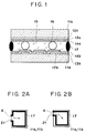
- Fig. 1 is schematic diagram showing an example of a ferroelectric liquid crystal cell of the invention.
- Reference numerals 11a and 11b denote glass substrates.
- Transparent electrodes 12a and 12b made of In2O3, ITO (Indium Tin Oxide), etc. are formed on the glass substrates.
- Insulative films (SiO2, film, TiO2 film, Ta2O5 film, etc.) 13a and 13b having thicknesses within a range from 200 to 3000 ⁇ and rubbing processed orientation control films 14a and 14b such as polyimide films or the like having thicknesses within a range from 50 to 1000 ⁇ are laminated on the transparent electrodes, respectively.
- a ferroelectric chiral smectic liquid crystal 15 is filled between the substrates 11a and 11b.
- a distance between the substrates 11a and 11b is set to a value within a range from 0.1 to 3 ⁇ m and is held by a beads spacer 16 (silica beads, alumina beads, etc.) arranged between both of the substrates.
- a beads spacer 16 silicon beads, alumina beads, etc.
- the substrates 11a and 11b are adhered by a sealing adhesive agent 17.
- the adhesive agent 17 is provided around the substrates and a part of the adhesive agent 17 is opened as an injection port 21 to inject liquid crystal.
- the inside of a panel is set into a vacuum, the liquid crystal is coated to the injection port, the injection port is sealed by the liquid crystal, a temperature of the liquid crystal panel is raised after that, and the liquid crystal is progressed into the panel, thereby injecting the liquid crystal.
- the orientation of the liquid crystal is largely influenced by the injecting state.
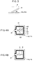
- the injection is influenced by the relation between an injecting direction A shown in Fig. 2 and a rubbing direction (not shown).
- the rubbing process is executed to the orientation control films 14a and 14b.
- a rubbing direction B denotes a direction in which a liquid crystal molecule is floating from the orientation surface by a pretilt angle ⁇ (5° or more).
- the rubbing direction B there are shown the injecting direction (processing direction) A, a -45° axis 41 corresponding to an axis which is inclined counterclockwise by 45° from the injecting direction A of the liquid crystal and a 45° axis 42 corresponding to an axis which is inclined clockwise by 45° from the injecting direction.
- the injecting direction A and the rubbing direction B intersect at an acute angle (intersection angle at this time lies within a range from 10° to 80°, preferably, 20° to 70°).
- the injecting direction A and the rubbing direction B are parallel to each other and are set in the same direction.
- the rubbing processing directions A used in cells of Figs. 4A and 4B are given to both of the substrates 11a and 11b and are parallel to each other and are set to the same direction.
- the rubbing directions given to the substrates 11a and 11b can be intersected at an acute angle, for instance, 3° to 30°, preferably, 3° to 10°. In this instance, it is desirable to decide the injecting direction for a central axis of the intersection angle as mentioned above.
- Two glass plates each having a thickness of 1.1 mm are prepared. Stripe-shaped electrodes made of ITO are formed on the glass substrates, respectively. Further, SiO2 films each having a thickness of 1000 ⁇ are formed as insulative films for prevention of short-circuits of the upper and lower electrodes by a sputtering method. A polyimide forming liquid LQ1802 (made by Hitachi Chemical co., Ltd.) is coated onto the SiO2 films by a spinner and is subjected to a heat burning process, thereby forming polyimide orientation films. The rubbing process is executed to the polyimide coating films after completion of the burning of the two substrates. The rubbing direction will be explained hereinlater.
- alumina beads whose average grain diameter is equal to about 1.5 ⁇ m are dispersed onto one of the substrates.
- an adhesive agent of an epoxy resin is formed onto the other substrate by a shape as shown in Fig. 2 by a screen printer. Two glass substrates are adhered and a panel is formed. A diagnosis size of the panel is equal to 14 inches.
- Figs. 5A to 5D show the relations between the rubbing direction B and the injecting direction A.
- the mixed ferroelectric liquid crystal containing phenylpyrimidine as a main component is injected into each of the above panels from the injection port.
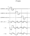
- Voltages of driving waveforms shown in Fig. 6 are applied to those matrix panels and the orientation uniformity of the whole panel is observed under cross nicols with respect to each of the panels. The results are shown below.
- the layer structures of the Sm*C phase are examined by an X-ray diffracting method by using an X-ray analyzing apparatus RAD-11B (45 kV, 30 mA).
- the cell has a chevron structure as shown in Fig. 7.
- An inclination angle ⁇ of the layer is equal to 10.5°.
- reference numerals 701 to 704 denote schematic diagrams showing arrangements of directions at respective positions between the substrates and show states in the cases where the directors are projected to the bottom surface of a cone and are seen from the direction of the bottom surface.
- Reference numerals 701 and 702 denote arrangements of the directors showing white and black two states of the spray orientation and 703 and 704 denote arrangements of the directors showing white and black two states of the uniform orientation.
- the orientations of the panels formed in the embodiments correspond to the uniform orientations shown by reference numerals 703 and 704.
- the domains of different contrasts occurring in the comparison examples correspond to a state in which the uniform orientation and the spray orientations shown by reference numerals 701 and 702 mixedly exist.
- the orientation uniformity in the panels E, F, and G, by setting the angle formed by the injecting direction and the rubbing direction to a value within a range from -45° to +45°, the orientation which is uniform as a whole can be obtained.
- the ferroelectric liquid crystal device of the orienting state which is uniform on the whole panel is derived.
- a ferroelectric liquid crystal device in which a pair of substrates and having electrodes are arranged so that the electrode surfaces face each other, a sealing agent is provided in the peripheral edge portions of the substrates, a liquid crystal injection port is opened in a part of the sealing agent, and a liquid crystal is injected from the injection port into a gap between both of the substrates.
- An intersection angle which is formed by the rubbing direction to orient the liquid crystal and the direction to inject the liquid crystal from the injection port lies within a range from -45° to +45°.
Landscapes
- Physics & Mathematics (AREA)
- Nonlinear Science (AREA)
- Mathematical Physics (AREA)
- Chemical & Material Sciences (AREA)
- Crystallography & Structural Chemistry (AREA)
- General Physics & Mathematics (AREA)
- Optics & Photonics (AREA)
- Liquid Crystal (AREA)
Applications Claiming Priority (2)
| Application Number | Priority Date | Filing Date | Title |
|---|---|---|---|
| JP81105/91 | 1991-03-22 | ||
| JP3081105A JP2835787B2 (ja) | 1991-03-22 | 1991-03-22 | 強誘電性液晶素子 |
Publications (3)
| Publication Number | Publication Date |
|---|---|
| EP0504911A2 true EP0504911A2 (de) | 1992-09-23 |
| EP0504911A3 EP0504911A3 (en) | 1993-01-20 |
| EP0504911B1 EP0504911B1 (de) | 1998-12-02 |
Family
ID=13737107
Family Applications (1)
| Application Number | Title | Priority Date | Filing Date |
|---|---|---|---|
| EP92104850A Expired - Lifetime EP0504911B1 (de) | 1991-03-22 | 1992-03-20 | Flüssigkristallvorrichtung |
Country Status (5)
| Country | Link |
|---|---|
| US (1) | US5657103A (de) |
| EP (1) | EP0504911B1 (de) |
| JP (1) | JP2835787B2 (de) |
| AT (1) | ATE174132T1 (de) |
| DE (1) | DE69227714T2 (de) |
Cited By (2)
| Publication number | Priority date | Publication date | Assignee | Title |
|---|---|---|---|---|
| CN1069976C (zh) * | 1994-02-14 | 2001-08-22 | 株式会社日立制作所 | 有源矩阵型液晶显示装置 |
| WO2010095758A1 (en) * | 2009-02-19 | 2010-08-26 | Nano Loa, Inc. | Process for filling a liquid crystal display device |
Families Citing this family (6)
| Publication number | Priority date | Publication date | Assignee | Title |
|---|---|---|---|---|
| JP2769060B2 (ja) * | 1991-11-20 | 1998-06-25 | アルプス電気株式会社 | 液晶表示素子の製造方法 |
| US5986736A (en) * | 1995-04-26 | 1999-11-16 | Canon Kabushiki Kaisha | Liquid crystal device, image display apparatus and image forming apparatus |
| TWI350397B (en) * | 2005-07-28 | 2011-10-11 | Sony Corp | Semi-transmissive liquid crystal display device |
| EP2947151A1 (de) | 2010-08-02 | 2015-11-25 | Regeneron Pharmaceuticals, Inc. | Bindeproteine mit vl-domänen |
| JP6900279B2 (ja) | 2016-09-13 | 2021-07-07 | キヤノン株式会社 | トナー及びトナーの製造方法 |
| JP7058534B2 (ja) * | 2018-03-27 | 2022-04-22 | シチズンファインデバイス株式会社 | 液晶パネル |
Family Cites Families (61)
| Publication number | Priority date | Publication date | Assignee | Title |
|---|---|---|---|---|
| US4367924A (en) * | 1980-01-08 | 1983-01-11 | Clark Noel A | Chiral smectic C or H liquid crystal electro-optical device |
| US4907859A (en) * | 1983-11-15 | 1990-03-13 | Canon Kabushiki Kaisha | Liquid crystal device and image forming apparatus utilizing liquid crystal device |
| JPS60107023A (ja) * | 1983-11-15 | 1985-06-12 | Canon Inc | 液晶装置 |
| JPS60156043A (ja) * | 1984-01-23 | 1985-08-16 | Canon Inc | カイラルスメクティック液晶素子 |
| US4712872A (en) * | 1984-03-26 | 1987-12-15 | Canon Kabushiki Kaisha | Liquid crystal device |
| JPS60220316A (ja) * | 1984-04-16 | 1985-11-05 | Canon Inc | 液晶光学素子 |
| JPS6134134U (ja) * | 1984-07-31 | 1986-03-01 | カシオ計算機株式会社 | 液晶装置 |
| US4682858A (en) * | 1984-08-20 | 1987-07-28 | Canon Kabushiki Kaisha | Liquid crystal device having reduced-pressure region in communication with ferroelectric liquid crystal |
| JPS6167832A (ja) * | 1984-09-12 | 1986-04-08 | Canon Inc | 液晶素子 |
| JPS6186732A (ja) * | 1984-10-04 | 1986-05-02 | Canon Inc | 液晶装置 |
| JPS61147232A (ja) * | 1984-12-20 | 1986-07-04 | Canon Inc | 液晶素子 |
| JPS61156229A (ja) * | 1984-12-28 | 1986-07-15 | Canon Inc | 液晶装置 |
| US4802740A (en) * | 1985-02-13 | 1989-02-07 | Canon Kabushiki Kaisha | Liquid crystal alignment layer containing polyvinyl-alcohol and titanium-alkoxide |
| US4721367A (en) * | 1985-04-01 | 1988-01-26 | Canon Kabushiki Kaisha | Liquid crystal device |
| JPS61231525A (ja) * | 1985-04-08 | 1986-10-15 | Hitachi Ltd | 強誘電性液晶素子とその製造方法 |
| US4898456A (en) * | 1985-04-23 | 1990-02-06 | Canon Kabushiki Kaisha | Liquid crystal optical device |
| JPS61260222A (ja) * | 1985-05-15 | 1986-11-18 | Canon Inc | 液晶素子 |
| US4844590A (en) * | 1985-05-25 | 1989-07-04 | Canon Kabushiki Kaisha | Method and apparatus for driving ferroelectric liquid crystal device |
| US4778259A (en) * | 1985-07-17 | 1988-10-18 | Canon Kabushiki Kaisha | Ferroelectric liquid crystal devices having reverse twist angle and stable states resulting from A.C. excitation |
| JP2647828B2 (ja) * | 1985-07-17 | 1997-08-27 | キヤノン株式会社 | 液晶素子の製造法 |
| DE3630012A1 (de) * | 1985-09-04 | 1987-04-23 | Canon Kk | Ferroelektrische fluessigkristallvorrichtung |
| JPH0685032B2 (ja) * | 1985-10-17 | 1994-10-26 | キヤノン株式会社 | カイラルスメクティック液晶素子 |
| JPS62119521A (ja) * | 1985-11-19 | 1987-05-30 | Canon Inc | 光学変調装置 |
| US4818078A (en) * | 1985-11-26 | 1989-04-04 | Canon Kabushiki Kaisha | Ferroelectric liquid crystal optical modulation device and driving method therefor for gray scale display |
| DE3688700T2 (de) * | 1985-12-18 | 1993-11-11 | Canon Kk | Flüssigkristallvorrichtung. |
| JP2654940B2 (ja) * | 1985-12-24 | 1997-09-17 | キヤノン株式会社 | 電気光学素子の製造方法 |
| US4712874A (en) * | 1985-12-25 | 1987-12-15 | Canon Kabushiki Kaisha | Ferroelectric liquid crystal device having color filters on row or column electrodes |
| GB2185614B (en) * | 1985-12-25 | 1990-04-18 | Canon Kk | Optical modulation device |
| US4820026A (en) * | 1986-03-20 | 1989-04-11 | Canon Kabushiki Kaisha | Ferroelectric liquid crystal device with modified polyvinyl alcohol alignment film |
| US4796979A (en) * | 1986-04-07 | 1989-01-10 | Canon Kabushiki Kaisha | Ferroelectric liquid crystal device having dual laminated alignment films |
| JPS62169325U (de) * | 1986-04-17 | 1987-10-27 | ||
| JPS62247326A (ja) * | 1986-04-21 | 1987-10-28 | Canon Inc | 強誘電性液晶素子の製造方法 |
| US4816178A (en) * | 1986-04-30 | 1989-03-28 | Canon Kabushiki Kaisha | Optically active compound and liquid crystal composition containing same |
| JPS62278540A (ja) * | 1986-05-27 | 1987-12-03 | Canon Inc | 液晶素子、その配向制御法及びその駆動法 |
| JPS62284334A (ja) * | 1986-06-03 | 1987-12-10 | Canon Inc | 液晶装置 |
| JPS62295021A (ja) * | 1986-06-16 | 1987-12-22 | Canon Inc | 液晶素子の製造方法 |
| JP2530432B2 (ja) * | 1986-07-22 | 1996-09-04 | キヤノン株式会社 | 液晶素子 |
| DE3750006T2 (de) * | 1986-08-25 | 1994-10-06 | Canon Kk | Optische Modulationsvorrichtung. |
| US4773738A (en) * | 1986-08-27 | 1988-09-27 | Canon Kabushiki Kaisha | Optical modulation device using ferroelectric liquid crystal and AC and DC driving voltages |
| US4917471A (en) * | 1986-08-30 | 1990-04-17 | Canon Kabushiki Kaisha | Liquid crystal device |
| US4879059A (en) * | 1986-09-02 | 1989-11-07 | Canon Kabushiki Kaisha | Liquid crystal device |
| JP2667816B2 (ja) * | 1986-09-20 | 1997-10-27 | キヤノン株式会社 | 液晶素子 |
| JPS6381324A (ja) * | 1986-09-26 | 1988-04-12 | Toshiba Corp | 液晶電気光学素子 |
| JP2739315B2 (ja) * | 1987-01-23 | 1998-04-15 | キヤノン株式会社 | カラーフィルターおよびカラー液晶素子 |
| JPS63220224A (ja) * | 1987-03-10 | 1988-09-13 | Seiko Epson Corp | 液晶電気光学装置 |
| US5000545A (en) * | 1987-05-28 | 1991-03-19 | Canon Kabushiki Kaisha | Liquid crystal device with metal electrode partially overlying transparent electrode |
| ATE131290T1 (de) * | 1987-06-12 | 1995-12-15 | Canon Kk | Vorrichtung mit einem ferroelektrischen flüssigkristall. |
| JP2770944B2 (ja) * | 1987-08-19 | 1998-07-02 | キヤノン株式会社 | 液晶素子 |
| US5268780A (en) * | 1989-05-11 | 1993-12-07 | Canon Kabushiki Kaisha | Liquid crystal device having a polyimide alignment film substituted with fluorine or a fluorine-containing group |
| AU606456B2 (en) * | 1987-09-17 | 1991-02-07 | Canon Kabushiki Kaisha | Ferroelectric smectic liquid crystal device |
| US4917473A (en) * | 1987-10-13 | 1990-04-17 | Semiconductor Energy Laboratory Co., Ltd. | Method of manufacturing liquid crystal devices |
| JPH01179915A (ja) * | 1988-01-11 | 1989-07-18 | Canon Inc | 液晶素子 |
| DE68928293T2 (de) * | 1988-06-23 | 1998-02-12 | Canon Kk | Vorrichtung mit einem Flüssigkristall |
| JP2728439B2 (ja) * | 1988-07-14 | 1998-03-18 | 毅 池田 | 4端子型ノイズフィルタおよびその製造方法 |
| US5132816A (en) * | 1989-02-02 | 1992-07-21 | Sharp Kabushiki Kaisha | Ferroelectric liquid crystal device and method of manufacturing the same |
| JPH02226115A (ja) * | 1989-02-28 | 1990-09-07 | Citizen Watch Co Ltd | 強誘電性液晶素子の製造方法 |
| JPH073047B2 (ja) * | 1989-06-20 | 1995-01-18 | 川鉄建材工業株式会社 | 矢板の打込方法および楔付き矢板 |
| JP2645754B2 (ja) * | 1989-10-26 | 1997-08-25 | キヤノン株式会社 | 液晶素子 |
| JP2830361B2 (ja) * | 1990-04-28 | 1998-12-02 | ソニー株式会社 | 光学活性化合物及びこれを用いた強誘電性液晶組成物 |
| JPH04258924A (ja) * | 1991-02-13 | 1992-09-14 | Canon Inc | カイラルスメクチック液晶素子およびその製造方法 |
| JPH0534697A (ja) * | 1991-07-25 | 1993-02-12 | Canon Inc | 強誘電性液晶表示素子 |
-
1991
- 1991-03-22 JP JP3081105A patent/JP2835787B2/ja not_active Expired - Fee Related
-
1992
- 1992-03-20 EP EP92104850A patent/EP0504911B1/de not_active Expired - Lifetime
- 1992-03-20 AT AT92104850T patent/ATE174132T1/de not_active IP Right Cessation
- 1992-03-20 DE DE69227714T patent/DE69227714T2/de not_active Expired - Fee Related
-
1995
- 1995-06-07 US US08/478,601 patent/US5657103A/en not_active Expired - Fee Related
Cited By (2)
| Publication number | Priority date | Publication date | Assignee | Title |
|---|---|---|---|---|
| CN1069976C (zh) * | 1994-02-14 | 2001-08-22 | 株式会社日立制作所 | 有源矩阵型液晶显示装置 |
| WO2010095758A1 (en) * | 2009-02-19 | 2010-08-26 | Nano Loa, Inc. | Process for filling a liquid crystal display device |
Also Published As
| Publication number | Publication date |
|---|---|
| JPH04294321A (ja) | 1992-10-19 |
| US5657103A (en) | 1997-08-12 |
| EP0504911A3 (en) | 1993-01-20 |
| ATE174132T1 (de) | 1998-12-15 |
| DE69227714D1 (de) | 1999-01-14 |
| EP0504911B1 (de) | 1998-12-02 |
| DE69227714T2 (de) | 1999-06-10 |
| JP2835787B2 (ja) | 1998-12-14 |
Similar Documents
| Publication | Publication Date | Title |
|---|---|---|
| US4740060A (en) | Electro-optical device having heat-bondable and non-heat-bondable gap controllers | |
| US5381256A (en) | Ferroelectric liquid crystal device with fine particles on insulator, having diameter less than substrate gap | |
| KR0161240B1 (ko) | 액정 배향 방법, 액정 배향 방법을 이용한 액정 소자 제조 방법, 그리고 액정 배향 방법을 이용하여 제조된 액정소자 | |
| JPH04258924A (ja) | カイラルスメクチック液晶素子およびその製造方法 | |
| JP2612503B2 (ja) | 液晶素子 | |
| US5657103A (en) | Liquid crystal device | |
| US5748274A (en) | LCD having a voltage being applied to the LC in the chiral nematic phase prior to the display driving | |
| JP2775527B2 (ja) | カイラルスメクチック液晶素子 | |
| US5568295A (en) | Chiral smetic LCD with small pretilt angle, substrate rubbed in two opposing directions, and no cholesteric phase or tilt angle > the pretilt plus inclination angles | |
| EP0500070B1 (de) | Flüssigkristallvorrichtung | |
| US5594571A (en) | Ferroelectric liquid crystal device and process for production thereof | |
| EP0525673B1 (de) | Flüssigkristallvorrichtung | |
| EP0532210B1 (de) | Flüssigkristallanzeige | |
| EP0775930A2 (de) | Flüssigkristallanzeigevorrichtung | |
| JPH11258613A (ja) | 液晶パネル用基板及び液晶表示素子 | |
| JP3184761B2 (ja) | 液晶素子、それを備えた画像表示装置及び画像形成装置 | |
| JP2645754B2 (ja) | 液晶素子 | |
| JPH06324339A (ja) | 強誘電性液晶素子 | |
| US5726725A (en) | Liquid crystal device and process for production thereof with polyimide alignment film rubbed and then baked | |
| JP2983724B2 (ja) | 強誘電性液晶素子の配向処理法 | |
| JP2775528B2 (ja) | カイラルスメクチック液晶素子 | |
| JP3029179B2 (ja) | 液晶素子 | |
| JP2612504B2 (ja) | 液晶装置 | |
| JPH0829788A (ja) | 液晶表示素子 | |
| JPH03138620A (ja) | 強誘電性液晶素子 |
Legal Events
| Date | Code | Title | Description |
|---|---|---|---|
| PUAI | Public reference made under article 153(3) epc to a published international application that has entered the european phase |
Free format text: ORIGINAL CODE: 0009012 |
|
| AK | Designated contracting states |
Kind code of ref document: A2 Designated state(s): AT BE CH DE DK ES FR GB GR IT LI LU NL PT SE |
|
| PUAL | Search report despatched |
Free format text: ORIGINAL CODE: 0009013 |
|
| AK | Designated contracting states |
Kind code of ref document: A3 Designated state(s): AT BE CH DE DK ES FR GB GR IT LI LU NL PT SE |
|
| 17P | Request for examination filed |
Effective date: 19930607 |
|
| 17Q | First examination report despatched |
Effective date: 19951020 |
|
| GRAG | Despatch of communication of intention to grant |
Free format text: ORIGINAL CODE: EPIDOS AGRA |
|
| GRAG | Despatch of communication of intention to grant |
Free format text: ORIGINAL CODE: EPIDOS AGRA |
|
| GRAH | Despatch of communication of intention to grant a patent |
Free format text: ORIGINAL CODE: EPIDOS IGRA |
|
| GRAH | Despatch of communication of intention to grant a patent |
Free format text: ORIGINAL CODE: EPIDOS IGRA |
|
| GRAA | (expected) grant |
Free format text: ORIGINAL CODE: 0009210 |
|
| AK | Designated contracting states |
Kind code of ref document: B1 Designated state(s): AT BE CH DE DK ES FR GB GR IT LI LU NL PT SE |
|
| PG25 | Lapsed in a contracting state [announced via postgrant information from national office to epo] |
Ref country code: IT Free format text: LAPSE BECAUSE OF FAILURE TO SUBMIT A TRANSLATION OF THE DESCRIPTION OR TO PAY THE FEE WITHIN THE PRE;WARNING: LAPSES OF ITALIAN PATENTS WITH EFFECTIVE DATE BEFORE 2007 MAY HAVE OCCURRED AT ANY TIME BEFORE 2007. THE CORRECT EFFECTIVE DATE MAY BE DIFFERENT FROM THE ONE RECORDED.SCRIBED TIME-LIMIT Effective date: 19981202 Ref country code: AT Free format text: LAPSE BECAUSE OF FAILURE TO SUBMIT A TRANSLATION OF THE DESCRIPTION OR TO PAY THE FEE WITHIN THE PRESCRIBED TIME-LIMIT Effective date: 19981202 Ref country code: GR Free format text: LAPSE BECAUSE OF NON-PAYMENT OF DUE FEES Effective date: 19981202 Ref country code: LI Free format text: LAPSE BECAUSE OF FAILURE TO SUBMIT A TRANSLATION OF THE DESCRIPTION OR TO PAY THE FEE WITHIN THE PRESCRIBED TIME-LIMIT Effective date: 19981202 Ref country code: NL Free format text: LAPSE BECAUSE OF FAILURE TO SUBMIT A TRANSLATION OF THE DESCRIPTION OR TO PAY THE FEE WITHIN THE PRESCRIBED TIME-LIMIT Effective date: 19981202 Ref country code: CH Free format text: LAPSE BECAUSE OF FAILURE TO SUBMIT A TRANSLATION OF THE DESCRIPTION OR TO PAY THE FEE WITHIN THE PRESCRIBED TIME-LIMIT Effective date: 19981202 Ref country code: BE Free format text: LAPSE BECAUSE OF FAILURE TO SUBMIT A TRANSLATION OF THE DESCRIPTION OR TO PAY THE FEE WITHIN THE PRESCRIBED TIME-LIMIT Effective date: 19981202 Ref country code: ES Free format text: THE PATENT HAS BEEN ANNULLED BY A DECISION OF A NATIONAL AUTHORITY Effective date: 19981202 |
|
| REF | Corresponds to: |
Ref document number: 174132 Country of ref document: AT Date of ref document: 19981215 Kind code of ref document: T |
|
| REG | Reference to a national code |
Ref country code: CH Ref legal event code: EP |
|
| REF | Corresponds to: |
Ref document number: 69227714 Country of ref document: DE Date of ref document: 19990114 |
|
| ET | Fr: translation filed | ||
| PG25 | Lapsed in a contracting state [announced via postgrant information from national office to epo] |
Ref country code: DK Free format text: LAPSE BECAUSE OF FAILURE TO SUBMIT A TRANSLATION OF THE DESCRIPTION OR TO PAY THE FEE WITHIN THE PRESCRIBED TIME-LIMIT Effective date: 19990302 Ref country code: SE Free format text: LAPSE BECAUSE OF FAILURE TO SUBMIT A TRANSLATION OF THE DESCRIPTION OR TO PAY THE FEE WITHIN THE PRESCRIBED TIME-LIMIT Effective date: 19990302 Ref country code: PT Free format text: LAPSE BECAUSE OF FAILURE TO SUBMIT A TRANSLATION OF THE DESCRIPTION OR TO PAY THE FEE WITHIN THE PRESCRIBED TIME-LIMIT Effective date: 19990302 |
|
| PG25 | Lapsed in a contracting state [announced via postgrant information from national office to epo] |
Ref country code: LU Free format text: LAPSE BECAUSE OF NON-PAYMENT OF DUE FEES Effective date: 19990320 |
|
| NLV1 | Nl: lapsed or annulled due to failure to fulfill the requirements of art. 29p and 29m of the patents act | ||
| REG | Reference to a national code |
Ref country code: CH Ref legal event code: PL |
|
| PLBE | No opposition filed within time limit |
Free format text: ORIGINAL CODE: 0009261 |
|
| STAA | Information on the status of an ep patent application or granted ep patent |
Free format text: STATUS: NO OPPOSITION FILED WITHIN TIME LIMIT |
|
| 26N | No opposition filed | ||
| REG | Reference to a national code |
Ref country code: GB Ref legal event code: IF02 |
|
| PGFP | Annual fee paid to national office [announced via postgrant information from national office to epo] |
Ref country code: FR Payment date: 20030310 Year of fee payment: 12 |
|
| PGFP | Annual fee paid to national office [announced via postgrant information from national office to epo] |
Ref country code: GB Payment date: 20030319 Year of fee payment: 12 |
|
| PGFP | Annual fee paid to national office [announced via postgrant information from national office to epo] |
Ref country code: DE Payment date: 20030327 Year of fee payment: 12 |
|
| PG25 | Lapsed in a contracting state [announced via postgrant information from national office to epo] |
Ref country code: GB Free format text: LAPSE BECAUSE OF NON-PAYMENT OF DUE FEES Effective date: 20040320 |
|
| PG25 | Lapsed in a contracting state [announced via postgrant information from national office to epo] |
Ref country code: DE Free format text: LAPSE BECAUSE OF NON-PAYMENT OF DUE FEES Effective date: 20041001 |
|
| GBPC | Gb: european patent ceased through non-payment of renewal fee |
Effective date: 20040320 |
|
| PG25 | Lapsed in a contracting state [announced via postgrant information from national office to epo] |
Ref country code: FR Free format text: LAPSE BECAUSE OF NON-PAYMENT OF DUE FEES Effective date: 20041130 |
|
| REG | Reference to a national code |
Ref country code: FR Ref legal event code: ST |