EP0488154A2 - Kontakt für Halbleiteranordnung und Verfahren zur Herstellung - Google Patents
Kontakt für Halbleiteranordnung und Verfahren zur Herstellung Download PDFInfo
- Publication number
- EP0488154A2 EP0488154A2 EP91120159A EP91120159A EP0488154A2 EP 0488154 A2 EP0488154 A2 EP 0488154A2 EP 91120159 A EP91120159 A EP 91120159A EP 91120159 A EP91120159 A EP 91120159A EP 0488154 A2 EP0488154 A2 EP 0488154A2
- Authority
- EP
- European Patent Office
- Prior art keywords
- diffused region
- forming
- region
- semiconductor device
- contact
- Prior art date
- Legal status (The legal status is an assumption and is not a legal conclusion. Google has not performed a legal analysis and makes no representation as to the accuracy of the status listed.)
- Granted
Links
Images


Classifications
-
- H—ELECTRICITY
- H10—SEMICONDUCTOR DEVICES; ELECTRIC SOLID-STATE DEVICES NOT OTHERWISE PROVIDED FOR
- H10D—INORGANIC ELECTRIC SEMICONDUCTOR DEVICES
- H10D62/00—Semiconductor bodies, or regions thereof, of devices having potential barriers
- H10D62/10—Shapes, relative sizes or dispositions of the regions of the semiconductor bodies; Shapes of the semiconductor bodies
- H10D62/13—Semiconductor regions connected to electrodes carrying current to be rectified, amplified or switched, e.g. source or drain regions
- H10D62/149—Source or drain regions of field-effect devices
- H10D62/151—Source or drain regions of field-effect devices of IGFETs
-
- H10W20/021—
-
- H10W20/0698—
-
- H—ELECTRICITY
- H01—ELECTRIC ELEMENTS
- H01L—SEMICONDUCTOR DEVICES NOT COVERED BY CLASS H10
- H01L2924/00—Indexing scheme for arrangements or methods for connecting or disconnecting semiconductor or solid-state bodies as covered by H01L24/00
- H01L2924/0001—Technical content checked by a classifier
- H01L2924/0002—Not covered by any one of groups H01L24/00, H01L24/00 and H01L2224/00
Definitions
- This invention relates to a semiconductor device, and more particularly to a semiconductor device including a MOS element, such as a semi-conductor device (hereinafter called "Bi-MOS element”) in which both a bipolar element and a MOS element are formed on a MOS field effect transistor (hereinafter called "MOSFET”) or a single semiconductor substrate and a method of manufacturing such semiconductor device.
- a MOS element such as a semi-conductor device (hereinafter called "Bi-MOS element”) in which both a bipolar element and a MOS element are formed on a MOS field effect transistor (hereinafter called "MOSFET”) or a single semiconductor substrate and a method of manufacturing such semiconductor device.
- MOSFET MOS field effect transistor
- a gate electrode and a source electrode and/or a drain electrode are formed during the growth and process of one and the same polycrystalline silicon, and a contact with a source diffused region or a drain diffused region (hereinafter called “source/drain diffused region”) is formed via a contact diffused region by impurity diffusion from the source/drain electrode.
- LDD Lightly Doped Drain
- MOSFET is an n-channel MOS transistor having an LDD structure.
- This MOSFET 100 has a buried contact structure on a p-type silicon substrate 10.
- a contact diffused region 28 constituting this buried contact structure is formed of an n+ diffusion layer formed by impurity diffusion from a source/drain electrode 40 formed of an n+-type polycrystalline silicon layer.
- the source/drain electrode 40 is formed together with a wiring portion 44 while the layer of a gate electrode 30 is formed.
- the n+-type contact diffused region 28 is connected to one n+-type ource/drain diffused region 42a via an n ⁇ -type offset region 52 which is located right under a side wall 50 contiguous to the source/drain electrode 40.
- reference numeral 12 designates a field oxide film; 14, a gate oxide film; and 18, a silicon layer hollow formed during etching the polycrystalline silicon layer.
- the semiconductor device of FIG. 2 has the following problems resulting from the buried contact structure:
- connection of the n+-type emitter diffused region should be shallow. Therefore, when forming a contact diffused region of MOSFET simultaneously with the emitter diffused region, the connection of the contact diffused region would be shallow to cause the above problems (1) and (2). Consequently, if in a Bi-MOS element an parasitic resistance resulting from the buried contact structure is to be reduced, the connection of the diffused region should be deep. This would be an obstacle to a high-speed Bi-MOS element.
- Another object of the invention is to provide a method of manufacturing the above-mentioned semi-conductor device.
- a MOS-type semiconductor device comprising:
- a Bi-MOS-type semiconductor device comprising:
- a method of manufacturing a MOS-type semiconductor device comprising the steps of:
- a method of manufacturing a Bi-MOS-type semiconductor device comprising the steps of:
- the diffused region forming the buried contact structure of the MOS element includes the first contact diffused region formed by impurity diffusion from the polycrystalline silicon layer and the second contact diffused region formed by diffusion deeper than the first contact diffused region, it is possible to realize a semiconductor device which hardly receives influence of non-uniform processing such as in the etching step, is stable in characteristic, has a low-resistance buried contact structure and has a low-parastic resistance.
- the MOS element of this invention since the MOS element of this invention has a deep diffusion layer to increase the area of connection of the source/drain, it is suitable for use in, for example, a static random access memory (SRAM).
- SRAM static random access memory
- characteristics such as resistance against noise, leak current and a ray soft error. This problem would be remarkable particularly on the side of the drain.
- the depth of connection and the impurity concentration of the second contact diffused region constituting the buried contact structure can be set independently of the impurity concentration in the polycrystalline silicon layer, it is possible to improve the degree of freedom of device designing.
- this MOS element is combined with a bipolar element, it is possible not only to achieve a high-speed operation of the bipolar element but also to realize a Bi-MOS element having a small parasitic resistance.
- the foregoing semiconductor devices can be manufactured in the same number of steps of production as conventional.
- FIG. 1 shows a semiconductor device schematically according to the first embodiment of this invention.
- This semiconductor device comprises an n-channel MOSFET 100 having an LDD structure.
- a field oxide film 12 and a gate oxide film 14 are formed on a p-type silicon substrate 10.
- a gate electrode 30 is formed, and a source/drain electrode 40 is formed at a position spaced from the gate electrode 30, and a wiring portion 44 is formed contiguously to the source/drain electrode 40.
- side walls 50 each in the form of a silicon oxide film is formed. Under each of the side walls 50, an n ⁇ -type offset region 52 constituting an LDD structure is formed.
- n+-type source/drain diffused regions 42a, 42b are formed on the opposite sides of the gate electrode 30.
- one n+-type source/drain diffused region 42a is connected with the source/drain electrode 40 by a buried contact structure 20.
- the buried contact structure 20 includes a first n+-type contact diffused region 22 formed shallowly on the surface of the silicon substrate 10, and a second n+-type contact diffused region 24 formed on the surface of the silicon substrate 10 more deeply than the first n+-type contact diffused region 22.
- the second n+-type contact diffused region 24 is formed by previous diffusion of phosphorous of a large diffusion constant as an impurity into the silicon substrate 10, with a part of the second n+-type contact diffused region 24 being connected to the source/drain diffused region 42a.
- the first n+-type contact diffused region 22 is formed by impurity diffusion of arsenic of a small diffusion contact from the source/drain electrode 40.
- the depth of the second n+-type contact diffused region 24 should be adequately large so that the contact resistance of the buried contact structure 20 can be reduced lower than a predetermined value.
- the first n+-type contact diffused region 22 may have a depth of diffusion of 0.1 to 0.3 ⁇ m
- the second n+-type contact diffused region 24 may have a depth of diffusion of 0.5 to 0.8 ⁇ m.
- the diffused region forming the buried contact structure 20 includes the first n+-type contact diffused region 22 formed by impurity diffusion of arsenic, and the second n+-type contact diffused region 24 formed by impurity diffusion of phosphorous deeper than the first contact diffused region 22. Because of this double-layer structure, it is possible to reduce the buried contact resistance, which would be a cause for the conventional problems, to an adequately small value, realizing a MOSFET having a small parasitic resistance.
- the MOSFET 100 allows the connecting area of the n+-type source/drain diffused region 42a to increase so that with the connection of the n+-type source/drain diffused resion 42a, 42b near the channel being kept shallow, adequate connection capacitance can be secured. Therefore the MOSFET 100 is suitable for use as a static random acess memory (SRAM).
- SRAM static random acess memory
- connection of the second N+-TYPE contact diffused region 24 is set to be deeper than the connection of the first n+-type contact diffused region 22, it is possible to obtain a low-resistance buried contact structure stably with no influence from the non-uniform processing, such as irregular depth of etching of the silicon substrate 10.
- the depth of connection and the impurity concentration of the second n+-type contact diffused region 24 can be set independently of the impurity concentration in the polycrystalline silicon layer, it is possible to improve the degree of freedom of device designing.
- the buried contact structure is formed only for one source/drain electrode.
- the buried contact structure may be formed for both the source and drain electrodes.
- FIGS. 4A through 4G shows the manufacturing process of the semiconductor device of FIG. 1.
- Like reference numerals designate similar parts or elements throughout FIGS. 1 and 4.
- Another MOSFET 300 according to the first embodiment, as shown in FIG. 3, can have a buried contact structure to which no LDD structure is added.
- This MOSFET 300 is essentially identical in structure with the LDD-type MOSFET 100 of FIG. 1, except that there is no region corresponding to the n ⁇ type offset region 52 of the MOSFET 100.
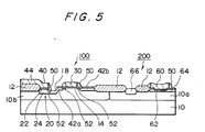
- FIG. 5 shows a semiconductor device according to the second embodiment of this invention.
- a Bi-MOS element includes an n-p-n-type vertical bipolar transistor 200 of washed emitter structure formed in an n-type well 10a on a p-type silicon substrate 10, and an n-channel MOSFET 100 of the LDD structure formed in a p-type well 10b.
- MOSFET 100 of this embodiment is identical in construction with the MOSFET 100 of the first embodiment. Therefore, like reference numerals designate similar parts or elements throughout FIGS. 1 and 5; its detailed description is omitted here for clarity.
- the bipolar transistor 200 includes an n+-type emitter diffused region 62 formed in the n-type well 10a, a p-type base diffused region 64 formed under the n+-type emitter diffused region 62, and an n+-type collector diffused region 66 located on the p-type base diffused region 64 via a field oxide film 12.
- An emitter electrode 60 is formed on the n+-type emitter diffused region 62.
- the n+-type emitter electrode 60 of the bipolar transistor 200, the n+-type gate electrode 30 of MOSFET 100, a source/drain electrode 40 and a wiring portion 44 connected to a buried contact region 20 are formed of the n+-type polycrystalline silicon layer having arsenic by the same layer forming process.
- a first n+-type contact diffused region 22 composing a buried contact structure 20 of MOSFET 100, and the n+-type emitter diffused region 62 of the bipolar transistor 200 are simultaneously formed by impurity diffusion of arsenic from the n+-type polycrystalline silicon layers (40, 60), having substantially the same depth of diffusion and impurity concentration.
- a second n+-type contact diffused region 24 composing the buried contact structure 20 of MOSFET 100 and the n+-type collector diffused region 66 for connecting the collector electrode of the bipolar transistor 200 are simultaneously formed by impurity diffusion of phosphorous, having substantially the same depth of diffusion and impurity concentration.
- the first n+-type contact diffused region 22 of MOSFET 100 has a depth of diffusion of 0.1 to 0.3 ⁇ m
- the second n+-type contact diffused region 24 has a depth of diffusion of 0.5 to 0.8 ⁇ m.
- the buried contact structure 20 of MOSFET 100 since the buried contact structure 20 of MOSFET 100 includes the first n+-type contact diffused region 22 formed by impurity diffusion and the second n+-type contact diffused region 24 formed by impurity diffusion deeper than the first contact diffused region 22, it is possible to reduce the resistance of the buried contact structure. Theretore it is possible to form on one substrate both MOSFET 100 having a small parasitic resistance and the high-speed bipolar transistor 200 with shallow diffusion.
- a buried contact structure having a low resistance can be formed with no influence by non-uniform processing, such as irregular depth of etching on the polycrystalline silicon layer as described in connection with the first embodiment.
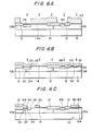
- FIGS. 6A through 6G shows the manufacturing process of the semiconductor device of FIG. 5
- Both the n+-type emitter diffused region 62 and the first n+-type contact diffused region 22 can be formed by the same first step, and the n+-type collector diffused region 66 and the second contact diffused region 24 are formed by the same second step, thus simplifying the manufacturing process of a semiconductor device.
- FIG. 7 shows a modification of the MOSFET of the first embodiment.
- MOSFET 400 of this embodiment is essentially identical in construction with the MOSFET 100 of FIG. 1, except that there is a cover portion 46.
- the cover portion 46 is formed by extending the end of the source/drain electrode 40 of the polycrystalline silicon layer, covering the gate oxide film 14.
- the cover portion 46 prevents the silicon layer of the first embodiment from being formed with a hollow 18, since the silicon substrate 10 is not exposed during etching. Therefore, no leak current is caused on the diffused layer due to the hollow 18.
- a masking film is formed on the silicon layer 16 at a cover portion forming region during etching (FIG. 4C).
- FIG. 8 shows a Bi-MOS element similar to the Bi-MOS element of the second embodiment, to which the structure of MOSFET 400 is used.
- the Bi-MOS element of this embodiment is identical with that of FIG. 5, except that the cover portion 46 is formed.
- MOSFET and Bi-MOS elements of this embodiment can offer an advantage that the cover portion 46 serves to assist in preventing the leak current in the diffused layer which leak current might be caused by etching. Therefore, it is possible not only to prevent the leak current in the buried contact structure but also to prevent the subthreashold characterics of MOSFET from being deteriorated.
- this invention is also applicable to p-n-p bipolar elements and/or p-channel MOS elements as well as the n-channel MOSFET as a MOS element and n-p-n bipolar transistor as the bipolar element.
Landscapes
- Insulated Gate Type Field-Effect Transistor (AREA)
- Metal-Oxide And Bipolar Metal-Oxide Semiconductor Integrated Circuits (AREA)
Applications Claiming Priority (12)
| Application Number | Priority Date | Filing Date | Title |
|---|---|---|---|
| JP328095/90 | 1990-11-28 | ||
| JP32809590 | 1990-11-28 | ||
| JP328096/90 | 1990-11-28 | ||
| JP32809690 | 1990-11-28 | ||
| JP32809690 | 1990-11-28 | ||
| JP32809590 | 1990-11-28 | ||
| JP12095891 | 1991-05-27 | ||
| JP12095891 | 1991-05-27 | ||
| JP12095991 | 1991-05-27 | ||
| JP12095991 | 1991-05-27 | ||
| JP120958/91 | 1991-05-27 | ||
| JP120959/91 | 1991-05-27 |
Publications (3)
| Publication Number | Publication Date |
|---|---|
| EP0488154A2 true EP0488154A2 (de) | 1992-06-03 |
| EP0488154A3 EP0488154A3 (en) | 1993-04-07 |
| EP0488154B1 EP0488154B1 (de) | 2002-04-24 |
Family
ID=27470736
Family Applications (1)
| Application Number | Title | Priority Date | Filing Date |
|---|---|---|---|
| EP91120159A Expired - Lifetime EP0488154B1 (de) | 1990-11-28 | 1991-11-26 | Kontakt für Halbleiteranordnung und Verfahren zur Herstellung |
Country Status (6)
| Country | Link |
|---|---|
| US (1) | US5315150A (de) |
| EP (1) | EP0488154B1 (de) |
| JP (1) | JP3144000B2 (de) |
| KR (1) | KR100232910B1 (de) |
| DE (1) | DE69132995T2 (de) |
| TW (1) | TW438049U (de) |
Families Citing this family (12)
| Publication number | Priority date | Publication date | Assignee | Title |
|---|---|---|---|---|
| EP0598168B1 (de) * | 1992-11-18 | 1997-05-28 | STMicroelectronics S.r.l. | Herstellung von direkte Kontakten in hoher Dichte MOS/CMOS Verfahren |
| US5541137A (en) * | 1994-03-24 | 1996-07-30 | Micron Semiconductor Inc. | Method of forming improved contacts from polysilicon to silicon or other polysilicon layers |
| US5466616A (en) * | 1994-04-06 | 1995-11-14 | United Microelectronics Corp. | Method of producing an LDMOS transistor having reduced dimensions, reduced leakage, and a reduced propensity to latch-up |
| US5525552A (en) * | 1995-06-08 | 1996-06-11 | Taiwan Semiconductor Manufacturing Company | Method for fabricating a MOSFET device with a buried contact |
| US5895766A (en) * | 1995-09-20 | 1999-04-20 | Micron Technology, Inc. | Method of forming a field effect transistor |
| US5652152A (en) * | 1996-04-22 | 1997-07-29 | Chartered Semiconductor Manufacturing Pte, Ltd. | Process having high tolerance to buried contact mask misalignment by using a PSG spacer |
| US5721146A (en) * | 1996-04-29 | 1998-02-24 | Taiwan Semiconductor Manufacturing Company Ltd | Method of forming buried contact architecture within a trench |
| US6211556B1 (en) * | 1998-04-23 | 2001-04-03 | Texas Instruments - Acer Incorporated | Eliminating buried contact trench in MOSFET devices having self-aligned silicide |
| US6153934A (en) * | 1998-07-30 | 2000-11-28 | International Business Machines Corporation | Buried butted contact and method for fabricating |
| JP2002198436A (ja) * | 2000-12-25 | 2002-07-12 | Sanyo Electric Co Ltd | 半導体集積回路装置およびその製造方法 |
| US7135373B2 (en) * | 2003-09-23 | 2006-11-14 | Texas Instruments Incorporated | Reduction of channel hot carrier effects in transistor devices |
| JP2014093739A (ja) * | 2012-11-06 | 2014-05-19 | Nagase Techno-Engineering Co Ltd | 集音装置 |
Family Cites Families (8)
| Publication number | Priority date | Publication date | Assignee | Title |
|---|---|---|---|---|
| NL7611774A (en) * | 1976-10-25 | 1978-02-28 | Philips Nv | FET prodn. from silicon semiconductor body - by forming inlaid oxide region having aperture in which the field effect structure is formed |
| JPS56134757A (en) * | 1980-03-26 | 1981-10-21 | Nec Corp | Complementary type mos semiconductor device and its manufacture |
| JPS60219771A (ja) * | 1984-04-16 | 1985-11-02 | Mitsubishi Electric Corp | Mos形半導体装置の製造方法 |
| JPS6113668A (ja) * | 1984-06-29 | 1986-01-21 | Hitachi Ltd | 半導体装置 |
| CA1258320A (en) * | 1985-04-01 | 1989-08-08 | Madhukar B. Vora | Small contactless ram cell |
| JPH01147829A (ja) * | 1987-12-04 | 1989-06-09 | Toshiba Corp | 半導体装置の製造方法 |
| JP2508818B2 (ja) * | 1988-10-03 | 1996-06-19 | 三菱電機株式会社 | 半導体装置の製造方法 |
| JPH03194974A (ja) * | 1989-12-22 | 1991-08-26 | Fuji Electric Co Ltd | Mos型半導体装置 |
-
1991
- 1991-11-18 JP JP03302126A patent/JP3144000B2/ja not_active Expired - Fee Related
- 1991-11-26 US US07/797,919 patent/US5315150A/en not_active Expired - Lifetime
- 1991-11-26 DE DE69132995T patent/DE69132995T2/de not_active Expired - Fee Related
- 1991-11-26 EP EP91120159A patent/EP0488154B1/de not_active Expired - Lifetime
- 1991-11-27 TW TW087200826U patent/TW438049U/zh not_active IP Right Cessation
- 1991-11-28 KR KR1019910021945A patent/KR100232910B1/ko not_active Expired - Fee Related
Also Published As
| Publication number | Publication date |
|---|---|
| HK1013890A1 (en) | 1999-09-10 |
| JPH0541486A (ja) | 1993-02-19 |
| DE69132995D1 (de) | 2002-05-29 |
| JP3144000B2 (ja) | 2001-03-07 |
| EP0488154A3 (en) | 1993-04-07 |
| KR100232910B1 (ko) | 1999-12-01 |
| DE69132995T2 (de) | 2002-10-31 |
| US5315150A (en) | 1994-05-24 |
| TW438049U (en) | 2001-05-28 |
| EP0488154B1 (de) | 2002-04-24 |
Similar Documents
| Publication | Publication Date | Title |
|---|---|---|
| US4965220A (en) | Method of manufacturing a semiconductor integrated circuit device comprising an MOS transistor and a bipolar transistor | |
| KR930008018B1 (ko) | 바이씨모스장치 및 그 제조방법 | |
| US4950617A (en) | Method of manufacturing semiconductor device | |
| US5082796A (en) | Use of polysilicon layer for local interconnect in a CMOS or BiCMOS technology incorporating sidewall spacers | |
| JPH05129429A (ja) | 半導体装置およびその製造方法 | |
| US5315150A (en) | Semiconductor device and method of manufacturing the same | |
| KR0166052B1 (ko) | 고전압 병합 바이폴라/cmos 및 그 제조 방법 | |
| US5128739A (en) | MIS type semiconductor device formed in a semiconductor substrate having a well region | |
| US5504024A (en) | Method for fabricating MOS transistors | |
| EP0399454B1 (de) | Monolithische Halbleiteranordnung mit CCD-, bipolaren und MOS-Strukturen | |
| JP3114654B2 (ja) | 半導体装置の製造方法 | |
| JPH07142419A (ja) | 半導体装置の製造方法 | |
| KR100292125B1 (ko) | 반도체기억장치및그제조방법 | |
| US6124180A (en) | BiCMOS process for counter doped collector | |
| US6917080B2 (en) | Bipolar transistor and semiconductor device using same | |
| JP3161435B2 (ja) | 半導体装置およびその製造方法 | |
| HK1013890B (en) | Contact for semiconductor device and method of manufacturing the same | |
| JPH0621357A (ja) | 逆電圧に強いバイポーラトランジスタの製造法 | |
| US6316324B1 (en) | Method of manufacturing semiconductor device without forming selective region by lithography | |
| JPH08293558A (ja) | 半導体装置およびその製造方法 | |
| JPH08227936A (ja) | 半導体装置及びその製造方法 | |
| EP0650190A1 (de) | Abhärtung gegen die Auslösung von Einzelereignissen für die VLSI-Technologie ohne die Schaltungen neu zu gestalten | |
| EP0398247A2 (de) | Halbleitervorrichtung und Verfahren zu seiner Herstellung | |
| JPH03184372A (ja) | 半導体装置の製造方法 | |
| JPH05129535A (ja) | 半導体集積回路とその製造方法 |
Legal Events
| Date | Code | Title | Description |
|---|---|---|---|
| PUAI | Public reference made under article 153(3) epc to a published international application that has entered the european phase |
Free format text: ORIGINAL CODE: 0009012 |
|
| AK | Designated contracting states |
Kind code of ref document: A2 Designated state(s): DE FR GB NL |
|
| PUAL | Search report despatched |
Free format text: ORIGINAL CODE: 0009013 |
|
| AK | Designated contracting states |
Kind code of ref document: A3 Designated state(s): DE FR GB NL |
|
| 17P | Request for examination filed |
Effective date: 19930813 |
|
| 17Q | First examination report despatched |
Effective date: 19941222 |
|
| RIC1 | Information provided on ipc code assigned before grant |
Free format text: 7H 01L 29/08 A, 7H 01L 29/772 B, 7H 01L 29/73 B, 7H 01L 29/06 B, 7H 01L 21/225 B |
|
| GRAG | Despatch of communication of intention to grant |
Free format text: ORIGINAL CODE: EPIDOS AGRA |
|
| RIC1 | Information provided on ipc code assigned before grant |
Free format text: 7H 01L 29/08 A, 7H 01L 29/78 B, 7H 01L 27/06 B, 7H 01L 21/336 B, 7H 01L 21/8249 B |
|
| GRAG | Despatch of communication of intention to grant |
Free format text: ORIGINAL CODE: EPIDOS AGRA |
|
| GRAH | Despatch of communication of intention to grant a patent |
Free format text: ORIGINAL CODE: EPIDOS IGRA |
|
| REG | Reference to a national code |
Ref country code: GB Ref legal event code: IF02 |
|
| GRAH | Despatch of communication of intention to grant a patent |
Free format text: ORIGINAL CODE: EPIDOS IGRA |
|
| GRAA | (expected) grant |
Free format text: ORIGINAL CODE: 0009210 |
|
| AK | Designated contracting states |
Kind code of ref document: B1 Designated state(s): DE FR GB NL |
|
| REG | Reference to a national code |
Ref country code: GB Ref legal event code: FG4D |
|
| REF | Corresponds to: |
Ref document number: 69132995 Country of ref document: DE Date of ref document: 20020529 |
|
| ET | Fr: translation filed | ||
| PLBE | No opposition filed within time limit |
Free format text: ORIGINAL CODE: 0009261 |
|
| STAA | Information on the status of an ep patent application or granted ep patent |
Free format text: STATUS: NO OPPOSITION FILED WITHIN TIME LIMIT |
|
| 26N | No opposition filed |
Effective date: 20030127 |
|
| PGFP | Annual fee paid to national office [announced via postgrant information from national office to epo] |
Ref country code: FR Payment date: 20061108 Year of fee payment: 16 |
|
| PGFP | Annual fee paid to national office [announced via postgrant information from national office to epo] |
Ref country code: NL Payment date: 20061115 Year of fee payment: 16 |
|
| PGFP | Annual fee paid to national office [announced via postgrant information from national office to epo] |
Ref country code: GB Payment date: 20061122 Year of fee payment: 16 |
|
| PGFP | Annual fee paid to national office [announced via postgrant information from national office to epo] |
Ref country code: DE Payment date: 20061123 Year of fee payment: 16 |
|
| GBPC | Gb: european patent ceased through non-payment of renewal fee |
Effective date: 20071126 |
|
| NLV4 | Nl: lapsed or anulled due to non-payment of the annual fee |
Effective date: 20080601 |
|
| PG25 | Lapsed in a contracting state [announced via postgrant information from national office to epo] |
Ref country code: DE Free format text: LAPSE BECAUSE OF NON-PAYMENT OF DUE FEES Effective date: 20080603 Ref country code: NL Free format text: LAPSE BECAUSE OF NON-PAYMENT OF DUE FEES Effective date: 20080601 |
|
| REG | Reference to a national code |
Ref country code: FR Ref legal event code: ST Effective date: 20080930 |
|
| PG25 | Lapsed in a contracting state [announced via postgrant information from national office to epo] |
Ref country code: GB Free format text: LAPSE BECAUSE OF NON-PAYMENT OF DUE FEES Effective date: 20071126 |
|
| PG25 | Lapsed in a contracting state [announced via postgrant information from national office to epo] |
Ref country code: FR Free format text: LAPSE BECAUSE OF NON-PAYMENT OF DUE FEES Effective date: 20071130 |