EP0477380B1 - Ausgangsschaltung eines abfühlverstärkers für einen halbleiterspeicher - Google Patents
Ausgangsschaltung eines abfühlverstärkers für einen halbleiterspeicher Download PDFInfo
- Publication number
- EP0477380B1 EP0477380B1 EP91906528A EP91906528A EP0477380B1 EP 0477380 B1 EP0477380 B1 EP 0477380B1 EP 91906528 A EP91906528 A EP 91906528A EP 91906528 A EP91906528 A EP 91906528A EP 0477380 B1 EP0477380 B1 EP 0477380B1
- Authority
- EP
- European Patent Office
- Prior art keywords
- signals
- equalize
- circuits
- output
- amplifiers
- Prior art date
- Legal status (The legal status is an assumption and is not a legal conclusion. Google has not performed a legal analysis and makes no representation as to the accuracy of the status listed.)
- Expired - Lifetime
Links
Images

Classifications
-
- G—PHYSICS
- G11—INFORMATION STORAGE
- G11C—STATIC STORES
- G11C7/00—Arrangements for writing information into, or reading information out from, a digital store
- G11C7/10—Input/output [I/O] data interface arrangements, e.g. I/O data control circuits, I/O data buffers
- G11C7/1051—Data output circuits, e.g. read-out amplifiers, data output buffers, data output registers, data output level conversion circuits
- G11C7/106—Data output latches
-
- G—PHYSICS
- G11—INFORMATION STORAGE
- G11C—STATIC STORES
- G11C7/00—Arrangements for writing information into, or reading information out from, a digital store
- G11C7/06—Sense amplifiers; Associated circuits, e.g. timing or triggering circuits
-
- G—PHYSICS
- G11—INFORMATION STORAGE
- G11C—STATIC STORES
- G11C7/00—Arrangements for writing information into, or reading information out from, a digital store
- G11C7/10—Input/output [I/O] data interface arrangements, e.g. I/O data control circuits, I/O data buffers
- G11C7/1048—Data bus control circuits, e.g. precharging, presetting, equalising
-
- G—PHYSICS
- G11—INFORMATION STORAGE
- G11C—STATIC STORES
- G11C7/00—Arrangements for writing information into, or reading information out from, a digital store
- G11C7/10—Input/output [I/O] data interface arrangements, e.g. I/O data control circuits, I/O data buffers
- G11C7/1051—Data output circuits, e.g. read-out amplifiers, data output buffers, data output registers, data output level conversion circuits
Definitions
- EP-A2-0 408 032 discloses a semiconductor memory device comprising a memory, an equalize circuit connected between first and second data lines to which data from the memory are outputted, for setting the data lines at an equal potential when an equalize pulse signal is applied to the equalize circuit, further comprising latch circuits for latching the potentials at the data lines, and buffer circuits provided on the input side of the latch circuits for cutting off the signals to the latch circuits according to the equalize pulse signals during the equalizing operation at the equalize circuit.
- Prior art document EP-A1-0 235 889 discloses a semiconductor memory device comprising: a first input terminal and a second input terminal for receiving complementary signals; a first and a second current mirror type sense amplifier, each of the current mirror type sense amplifiers including: a reference node; an output terminal; a first transistor connected with the reference node; and a second transistor connected with the output terminal.
- the gates of the first transistor of the first sense amplifier and of the second transistor of the second sense amplifier are connected to the first input terminal, and the gates of the second transistor of the first sense amplifier and of the first transistor of the second sense amplifier are connected to the second input terminal.
- a first short-circuiting transistor is connected between the reference nodes and able to conduct temporarily upon receipt of a clock signal at its gate to speed up the read out operation of a static random access memory.
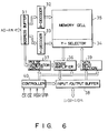
- FIG. 6 illustrates an important part of a conventional semiconductor memory device such as an EPROM.
- This semiconductor memory device comprises: for example, an address buffer 31 that stores the data read address signal temporarily; an X-decoder 32 and a Y-decoder 33 that decode the address signal from the address buffer 31; a Y-selector 34 that receives the output of the Y-decoder 33; a memory cell unit 35 from which a particular cell is selected depending on the outputs of the Y-selector 34 and X-decoder 32; a sense amplifier 36 that amplifies the signal read out of the memory cell unit 35 and supplied from the Y-selector 34 and produces a data signal with a specified level; a pulse generator circuit (ATD) 37 that senses the change of address signal in the address buffer 31, generates a specified pulse signal (hereinafter, referred to as an equalizer pulse signal), and supplies it to the sense amplifier 36; an input/output buffer circuit 38 that outputs the data signal from the sense amplifier 36; a
- the memory cell unit 35 is composed of, for example, a referential EPROM and designed to allow the simultaneous reading of signals of different levels.
- the sense amplifier 36 is designed to produce signals of a specified level by, for example, three-stage amplification of different-level signals from the memory cell unit 35 via the Y-selector 34.
- Each of the first through third stage amplifying sections is made up of a pair of differential amplifiers and a transfer gate circuit that equalizes the outputs of the differential amplifier pair to the same level on the basis of the equalize pulse signal from the pulse generator circuit 37.
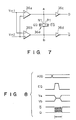
- Figure 7 illustrates the construction of the third-stage amplifying section and output circuit.
- the differential amplifiers 36a and 36b compare the signals from the second-stage amplifying section (not shown) for potential difference and judge whether the signal is at the "1" or "0" level. These differential amplifiers 36a and 36b are supplied with input signals so as to each produce signals of different levels, that is, the output level of the differential amplifier 36b is "0" when the output level of the differential amplifier 36a is "1". Specifically, the input signal V in1 is supplied to both the non-inverted input terminal of the differential amplifier 36a and the inverted terminal of the differential amplifier 36b, while the input signal V in2 is supplied to both the non-inverted input terminal of the differential amplifier 36b and the inverted terminal of the differential amplifier 36a.
- the output terminals of the differential amplifiers 36a and 36b are connected to inverter circuits 36c and 36d, respectively.
- a transfer gate 36e consisting of a p-channel transistor P1 and an n-channel transistor N1 connected in parallel.
- the gates of the n-channel transistor N1 and p-channel transistor P1 are supplied with the equalize pulse signals EQ and /EQ from the pulse generating circuit 37, respectively.
- the pulse generator circuit 37 produces the equalize pulse signals EQ and /EQ. Then, the transistors P1 and N1 receiving the equalize pulses EQ and /EQ turn conductive, thereby equalizing the potentials Va and Vb of both nodes a and b.
- the transistors P1 and N1 become non-conductive, which allows the potentials Va and Vb of the output nodes a and b of the differential amplifiers 36a and 36b to return to the original potentials at which the amplifiers 36a and 36b judged the nodes to be.
- the equalize pulse signals EQ and /EQ make the transistors P1 and N1 conductive, the potentials Va and Vb of the output terminals of the differential amplifiers 36a and 36b are at an intermediate potential. Therefore, the inverter circuits 36c and 36d cannot determine whether the input potentials are at the "0" or "1" level, which makes the output potentials Q and /Q indeterminate, leading to a possibility of producing erroneous outputs.
- the object of the present invention is to provide a semiconductor memory device which can maintain the output signal stably at a specified level even in the presence of equalize pulse signals and achieve high-speed operation by shortening the time from when the equalize pulse signal ceases till a normal signal appears.
- a semiconductor memory device that contains amplifiers for generating equalize pulse signals according to the change of address and based on the equalize pulse signals, separately amplifying a pair of signals read from the memory, and an equalize circuit for equalizing the output signal of the amplifier, and further contains latch circuits for latching the output signals from the amplifiers; and cut-off circuits that are provided on the input side of the latch circuits and during the equalizing operation at the equalize circuit, cut off the signals to the latch circuits according to the equalize pulse signals.
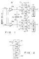
- Figure 1 illustrates the third-stage amplifying section of the sense amplifier 36.
- the same parts as those in Fig. 7 are indicated by the same reference characters, and explanation will be focused mainly on parts different from those of Fig. 7.
- the output terminals of the differential amplifiers 36a and 36b are connected to latch circuits 13 and 14 via clocked (CMOS) inverter circuits 11 and 12, respectively.
- CMOS clocked
- the latch circuits 13 and 14 latch the signals that have been judged at the differential amplifiers 36a and 36b.
- the clocked inverter circuits 11 and 12 have the same configuration, so that only the construction of the inverter circuit 11 will be explained, and for the inverter circuit 12, the same parts as those of the inverter circuit 11 are indicated by the same reference characters and their explanation will be omitted.
- the clocked inverter circuit 11 is composed of a series connection of the current paths of p-channel transistors P2 and P3 and n-channel transistors N2 and N3 between the power supply V and the ground.
- the gates of the p-channel transistor P2 and n-channel transistor N2 are connected to the output terminal of the differential amplifier 36a.
- the drains of the transistor P2 and transistor N2 are connected to the input terminal of the latch circuit 13.
- the source of the transistor P2 is connected to the drain of the p-channel transistor P3 whose gate receives the equalize pulse signal EQ and whose source is connected to the power supply V.
- the source of the transistor N2 is connected to the drain of the n-channel transistor N3 whose gate receives the equalize pulse signal /EQ and whose source is connected to the ground.
- FIG. 1 illustrates the construction of the latch circuits 13 and 14.
- the latch circuits 13 and 14 are each made up of two CMOS inverter circuits IN1 and IN2.
- the inverter circuits IN1 and IN2 consist of p-channel and n-channel transistors P4 and N4, and P5 and N5, respectively.
- the transistors P3 and N3 of the clocked inverter circuits 11 and 12 are in the conducting state. In this state, depending on the potentials Va and Vb of the output terminals of the differential amplifiers 36a and 36b, the output potentials Vc and Vd of the clocked inverter circuits 11 and 12 are at the "0" level and "1" level, respectively, which are latched at the latch circuits 13 and 14. As a result, the output potentials Q and /Q of the latch circuits 13 and 14 are at the "0" level and "1" level, respectively.
- the transistors P1 and N1 Upon termination of the equalize pulse signals EQ and /EQ, the transistors P1 and N1 turn non-conductive, whereas the transistors P3 and N3 turn conductive, capable of supplying subsequent signals.
- the clocked inverter circuits 11 and 12 do not transfer signals and instead, the latch circuits 13 and 14 supply the signals latched before the generation of the equalize pulse signals, as Q and /Q. This eliminates an unstable state found in a conventional equivalent, which ensures the reliable output of a signal of a specified level.
- the output potentials Va and Vb of the differential amplifiers 36a and 36b (referred to as the potentials of nodes a and b) undergo a slight instability temporarily.
- the cause of this is that the nodes a and b are connected to the gates of the transistors P2 and N2 constituting the clocked inverter circuits 11 and 12.
- the latch circuits 13 and 14 each consisting of two inverter circuits IN1 and IN2 as shown in Fig. 2, hold the previous data.
- the transistor P4 making up the inverter circuit IN1, conductive to output a "1" level signal
- the transistor N5 making up the inverter circuit IN2 is on, which allows the latch circuit 13 to remain at the "1" level.
- the transistor P2 in the clocked inverter circuit 11 is partially conductive as stated above, a conducting path from the node K1, connecting the transistors P2 and P3, through the transistor P2 to the transistor N5 is created, reducing the potential of the node K1.
- the potential Va of the node a tends to return to the "1" level, but because the parasitic capacitance C1 (the gate capacitance + the junction capacitance) between the node K1 and the gate of the transistor P2 is at a low level, the potential of the node a begins to fall temporarily.
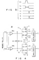
- Figure 4 shows a second embodiment of the present invention, which solves the problem of loss of time in the first embodiment.
- the same parts as those in Fig. 1 are indicated by the same reference characters and the explanation will center on the parts different from the first embodiment.
- the output terminals of the differential amplifiers 36a and 36b are connected to the gates of the transistors P3 and N3 constituting the clocked inverter circuits 11 and 12.
- the gates of transistors P2 and N2 are supplied with the equalize pulse signals EQ and /EQ, respectively.
- the transistors P2 and N2 of the clocked inverter circuits 11 and 12 can be put in a completely non-conductive state.
- the conducting path from the node K1 through the transistor P2 to the transistor P5, making up the latch circuit 13 can be cut off, which prevents the potential of the node K1 from dropping even when the potential of the node a is at an intermediate potential. Therefore, when the equalize pulse signals EQ and /EQ cease and the potential of the node a returns to its original potential, different pieces of data are prevented from temporarily appearing, which makes it possible to transfer data reliably at high speed.
- EPROMs While in the embodiments, the present invention is applied to EPROMs, it is not restricted to this. For example, it may be applicable to SRAMs.
- the present invention can maintain the output signal stably at a specified level even in the presence of the equalize pulse signal, and achieve a high-speed operation by shortening the time from when the equalize signal ceases till a normal signal appears. This feature is useful for sense amplifiers and its industrial applicability is high.
Landscapes
- Static Random-Access Memory (AREA)
- Dram (AREA)
- Read Only Memory (AREA)
Claims (4)
- Halbleiterspeichervorrichtung mit:einem ersten und einen zweiten Verstärker (36a,36b) zum Verstärkern eines Paares komplementärer Signale, die aus dem Speicher (35) ausgelesen werden;einer Ausgleichsschaltung (36e), die über die Ausgangsklemmen des ersten und zweiten Verstärkers (36a,36b) geschaltet ist, und die Potentiale der Ausgangsklemmen der ersten und zweiten Verstärker (36a,36b) auf der Grundlage von Ausgleichsimpulssignalen (EQ,/EQ) ausgleicht, die entsprechend der Änderung einer Adresse zum Zugriff auf Daten in dem Speicher (35) erzeugt werden;Zwischenspeicherschaltungen (13,14) zum Zwischenspeichern der Ausgangssignale von den Verstärkern (36a,36b); undAbschneideschaltungen (11,12), die auf der Eingangsseite der Zwischenspeicherschaltungen (13,14) vorgesehen sind, und während des Ausgleichsvorgangs der Ausgleichsschaltung (36e) die Signale zu den Zwischenspeicherschaltungen (13,14) entsprechend den Ausgleichsimpulssignalen (EQ,/EQ) abschneiden.
- Halbleiterspeichervorrichtung nach Anspruch 1,
dadurch gekennzeichnet, daß
jede der Abschneideschaltungen (11,12) aus einer getakteten Inverterschaltung besteht, die in eine Zustand hoher Impedanz versetzt wird, wenn sie das Ausgleichsimpulssignal (EQ,/EQ) empfängt. - Halbleiterspeichervorrichtung nach Anspruch 2,
dadurch gekennzeichnet, daß
jede der getakteten Inverterschaltungen (11,12) aus ersten MOS-Transistoren (P2,N2) eines ersten und zweiten Leitfähigkeitstyps besteht, deren Gates jeweils die Ausgangssignale der Verstärker (36a,36b) empfangen, und deren eines Ende von deren Strompfaden an die Eingangsklemme jeder der Zwischenspeicherschaltungen (13,15) angeschlossen ist, und aus zweiten MOS-Transistoren (P3,N3) eines ersten und zweiten Leitfähigkeitstyps, bei denen ein Ende jedes ihrer Strompfade an das andere Ende jedes der Strompfade der ersten MOS-Transistoren (P2,N2) angeschlossen ist, und deren Gates die Ausgleichsimpulssignale (EQ, /EQ) empfangen. - Halbleiterspeichervorrichtung nach Anspruch 2,
dadurch gekennzeichnet, daß
jede der getakteten Inverterschaltungen (11,12) aus ersten MOS-Transistoren (P2,N2) eines ersten und zweiten Leitfähigkeitstyps besteht, deren Gates jeweils die Ausgleichsimpulssignale (EQ,/EQ) empfangen, und deren eines Ende ihrer Strompfade an die Eingangsklemme jeder der Zwischenspeicherschaltungen (13,14) angeschlossen ist, und aus zweiten MOS-Transistoren (P3,N3) eines ersten und zweiten Leitfähigkeitstpys, deren eines Ende ihrer Strompfade an das andere Ende jedes der Strompfade der ersten MOS-Transistoren (P2,N2) angeschlossen ist, und deren Gates jeweils die Ausgangssignale von den Verstärkern (36a,36b) erhalten.
Applications Claiming Priority (3)
| Application Number | Priority Date | Filing Date | Title |
|---|---|---|---|
| JP83945/90 | 1990-03-30 | ||
| JP8394590A JP2573392B2 (ja) | 1990-03-30 | 1990-03-30 | 半導体記憶装置 |
| PCT/JP1991/000406 WO1991015856A1 (fr) | 1990-03-30 | 1991-03-28 | Circuit de sortie pour amplificateur de lecture utilise dans une memoire a semiconducteurs |
Publications (3)
| Publication Number | Publication Date |
|---|---|
| EP0477380A1 EP0477380A1 (de) | 1992-04-01 |
| EP0477380A4 EP0477380A4 (en) | 1992-09-16 |
| EP0477380B1 true EP0477380B1 (de) | 1996-05-22 |
Family
ID=13816725
Family Applications (1)
| Application Number | Title | Priority Date | Filing Date |
|---|---|---|---|
| EP91906528A Expired - Lifetime EP0477380B1 (de) | 1990-03-30 | 1991-03-28 | Ausgangsschaltung eines abfühlverstärkers für einen halbleiterspeicher |
Country Status (6)
| Country | Link |
|---|---|
| US (1) | US5325328A (de) |
| EP (1) | EP0477380B1 (de) |
| JP (1) | JP2573392B2 (de) |
| KR (1) | KR940004520B1 (de) |
| DE (1) | DE69119679T2 (de) |
| WO (1) | WO1991015856A1 (de) |
Families Citing this family (19)
| Publication number | Priority date | Publication date | Assignee | Title |
|---|---|---|---|---|
| US5331228A (en) * | 1992-07-31 | 1994-07-19 | Sgs-Thomson Microelectronics, Inc. | Output driver circuit |
| JP2768880B2 (ja) * | 1993-01-19 | 1998-06-25 | 株式会社東芝 | 半導体記憶装置 |
| GB2286072B (en) * | 1994-01-31 | 1998-02-25 | Advanced Risc Mach Ltd | Sense amplification in data memories |
| JP3067094B2 (ja) * | 1995-02-22 | 2000-07-17 | 三洋電機株式会社 | 光再生装置 |
| US5914899A (en) * | 1995-07-05 | 1999-06-22 | Kabushiki Kaisha Toshiba | Semiconductor memory having a page mode in which previous data in an output circuit is reset before new data is supplied |
| JPH0922593A (ja) * | 1995-07-05 | 1997-01-21 | Toshiba Microelectron Corp | 半導体メモリ |
| JP3192077B2 (ja) * | 1996-01-30 | 2001-07-23 | 日本電気株式会社 | 半導体記憶装置 |
| US5644538A (en) * | 1996-03-01 | 1997-07-01 | Micron Technology, Inc. | Circuit and method for controllng the duration of pulses in a control signal from an electronic system |
| US6225888B1 (en) * | 1997-12-08 | 2001-05-01 | Nokia Telecommunications Oy | Authentication between communicating parties in a telecommunications network |
| JP2001118388A (ja) * | 1999-10-18 | 2001-04-27 | Nec Ic Microcomput Syst Ltd | バッファ回路 |
| US6603817B1 (en) * | 2000-03-21 | 2003-08-05 | Mitsubisihi Denki Kabushiki Kaisha | Buffer circuit capable of correctly transferring small amplitude signal in synchronization with high speed clock signal |
| DE10031947B4 (de) * | 2000-06-30 | 2006-06-14 | Infineon Technologies Ag | Schaltungsanordnung zum Ausgleich unterschiedlicher Spannungen auf Leitungszügen in integrierten Halbleiterschaltungen |
| JP4313537B2 (ja) * | 2001-02-02 | 2009-08-12 | 富士通株式会社 | 低振幅電荷再利用型低電力cmos回路装置、加算器回路及び加算器モジュール |
| US20060250162A1 (en) * | 2005-04-18 | 2006-11-09 | Samsung Electronics Co., Ltd. | Signal amplification circuit for high-speed operation and semiconductor memory device having the same |
| JP4901211B2 (ja) * | 2005-12-26 | 2012-03-21 | 株式会社東芝 | センスアンプ及び半導体記憶装置 |
| CN101416230B (zh) * | 2006-05-24 | 2011-12-14 | 夏普株式会社 | 显示装置 |
| KR100824779B1 (ko) * | 2007-01-11 | 2008-04-24 | 삼성전자주식회사 | 반도체 메모리 장치의 데이터 출력 경로 및 데이터 출력방법 |
| CN101118780B (zh) * | 2007-09-18 | 2010-09-08 | 钰创科技股份有限公司 | 一种具有感测放大器的闩锁器 |
| US10204906B2 (en) * | 2016-12-16 | 2019-02-12 | Intel Corporation | Memory with single-event latchup prevention circuitry |
Citations (1)
| Publication number | Priority date | Publication date | Assignee | Title |
|---|---|---|---|---|
| EP0408032A2 (de) * | 1989-07-12 | 1991-01-16 | Kabushiki Kaisha Toshiba | Steuerschaltung für den Datenausgang für eine Halbleiterspeicheranordnung |
Family Cites Families (11)
| Publication number | Priority date | Publication date | Assignee | Title |
|---|---|---|---|---|
| JPS595986B2 (ja) * | 1976-06-21 | 1984-02-08 | 株式会社東芝 | Mosランダムアクセスメモリ |
| JPS5429531A (en) * | 1977-08-09 | 1979-03-05 | Sharp Corp | Sense circuit for cmos static random access memory |
| JPS60164997A (ja) * | 1984-02-08 | 1985-08-28 | Toshiba Corp | 読出し専用半導体記憶回路 |
| JPS62167698A (ja) * | 1986-01-20 | 1987-07-24 | Fujitsu Ltd | 半導体記億装置 |
| JPS6350997A (ja) * | 1986-08-19 | 1988-03-03 | Toshiba Corp | 出力バツフア回路 |
| JPS63209212A (ja) * | 1987-02-25 | 1988-08-30 | Hitachi Ltd | ラツチドライバ回路 |
| US4891792A (en) * | 1987-09-04 | 1990-01-02 | Hitachi, Ltd. | Static type semiconductor memory with multi-stage sense amplifier |
| JPH01290191A (ja) * | 1988-05-17 | 1989-11-22 | Ricoh Co Ltd | センスアンプ回路装置 |
| JP2573335B2 (ja) * | 1988-11-09 | 1997-01-22 | 株式会社東芝 | 不揮発性メモリ |
| US5126974A (en) * | 1989-01-20 | 1992-06-30 | Hitachi, Ltd. | Sense amplifier for a memory device |
| JP2534782B2 (ja) * | 1989-11-10 | 1996-09-18 | 株式会社東芝 | 半導体装置 |
-
1990
- 1990-03-30 JP JP8394590A patent/JP2573392B2/ja not_active Expired - Lifetime
-
1991
- 1991-03-28 EP EP91906528A patent/EP0477380B1/de not_active Expired - Lifetime
- 1991-03-28 US US07/777,335 patent/US5325328A/en not_active Expired - Lifetime
- 1991-03-28 WO PCT/JP1991/000406 patent/WO1991015856A1/ja not_active Ceased
- 1991-03-28 DE DE69119679T patent/DE69119679T2/de not_active Expired - Fee Related
- 1991-03-29 KR KR1019910004962A patent/KR940004520B1/ko not_active Expired - Lifetime
Patent Citations (1)
| Publication number | Priority date | Publication date | Assignee | Title |
|---|---|---|---|---|
| EP0408032A2 (de) * | 1989-07-12 | 1991-01-16 | Kabushiki Kaisha Toshiba | Steuerschaltung für den Datenausgang für eine Halbleiterspeicheranordnung |
Also Published As
| Publication number | Publication date |
|---|---|
| US5325328A (en) | 1994-06-28 |
| JPH03283194A (ja) | 1991-12-13 |
| EP0477380A4 (en) | 1992-09-16 |
| EP0477380A1 (de) | 1992-04-01 |
| KR940004520B1 (ko) | 1994-05-25 |
| DE69119679T2 (de) | 1996-10-31 |
| JP2573392B2 (ja) | 1997-01-22 |
| DE69119679D1 (de) | 1996-06-27 |
| WO1991015856A1 (fr) | 1991-10-17 |
Similar Documents
| Publication | Publication Date | Title |
|---|---|---|
| EP0477380B1 (de) | Ausgangsschaltung eines abfühlverstärkers für einen halbleiterspeicher | |
| KR100194741B1 (ko) | 반도체집적회로 | |
| US5068831A (en) | Data read circuit for semiconductor storage device | |
| KR100394573B1 (ko) | 반도체 메모리장치의 센스앰프회로 | |
| US7038962B2 (en) | Semiconductor integrated circuit | |
| US5798972A (en) | High-speed main amplifier with reduced access and output disable time periods | |
| US4658160A (en) | Common gate MOS differential sense amplifier | |
| US5729499A (en) | Sense amplifier and reading circuit with sense amplifier | |
| KR950005171B1 (ko) | 전류 미러 증폭회로 및 그의 구동 방법 | |
| KR100299522B1 (ko) | 고속 센스 증폭기 | |
| US5646892A (en) | Data reading circuit | |
| EP0443776B1 (de) | Abfühlschaltung für nichtflüchtige Speicheranordnung | |
| KR100321157B1 (ko) | 래치형 센스 앰프 | |
| KR100301604B1 (ko) | 감지 증폭기 회로 | |
| JP3016757B2 (ja) | アドレス遷移検出回路 | |
| KR19990016994A (ko) | 반도체 메모리장치 | |
| JPH05242682A (ja) | 差動増幅回路 | |
| KR0178882B1 (ko) | 증폭회로 | |
| KR100240523B1 (ko) | 반도체 집적 회로 장치 | |
| KR100244433B1 (ko) | 래치 형태의 센스 증폭기 | |
| KR0146171B1 (ko) | 감지 증폭기용 구동전압 발생기 | |
| CN118072789A (zh) | 灵敏放大器电路以及阻变存储器装置 | |
| JPH087575A (ja) | センスアンプ及び半導体記憶装置 | |
| JPH09172334A (ja) | センスアンプ | |
| KR20030023339A (ko) | 반도체 메모리 장치 |
Legal Events
| Date | Code | Title | Description |
|---|---|---|---|
| PUAI | Public reference made under article 153(3) epc to a published international application that has entered the european phase |
Free format text: ORIGINAL CODE: 0009012 |
|
| 17P | Request for examination filed |
Effective date: 19911129 |
|
| AK | Designated contracting states |
Kind code of ref document: A1 Designated state(s): DE FR GB |
|
| A4 | Supplementary search report drawn up and despatched |
Effective date: 19920730 |
|
| AK | Designated contracting states |
Kind code of ref document: A4 Designated state(s): DE FR GB |
|
| 17Q | First examination report despatched |
Effective date: 19940824 |
|
| GRAA | (expected) grant |
Free format text: ORIGINAL CODE: 0009210 |
|
| AK | Designated contracting states |
Kind code of ref document: B1 Designated state(s): DE FR GB |
|
| REF | Corresponds to: |
Ref document number: 69119679 Country of ref document: DE Date of ref document: 19960627 |
|
| ET | Fr: translation filed | ||
| PGFP | Annual fee paid to national office [announced via postgrant information from national office to epo] |
Ref country code: GB Payment date: 19970319 Year of fee payment: 7 |
|
| PLBE | No opposition filed within time limit |
Free format text: ORIGINAL CODE: 0009261 |
|
| STAA | Information on the status of an ep patent application or granted ep patent |
Free format text: STATUS: NO OPPOSITION FILED WITHIN TIME LIMIT |
|
| 26N | No opposition filed | ||
| PGFP | Annual fee paid to national office [announced via postgrant information from national office to epo] |
Ref country code: FR Payment date: 19980310 Year of fee payment: 8 |
|
| PG25 | Lapsed in a contracting state [announced via postgrant information from national office to epo] |
Ref country code: GB Free format text: LAPSE BECAUSE OF NON-PAYMENT OF DUE FEES Effective date: 19980328 |
|
| GBPC | Gb: european patent ceased through non-payment of renewal fee |
Effective date: 19980328 |
|
| PG25 | Lapsed in a contracting state [announced via postgrant information from national office to epo] |
Ref country code: FR Free format text: LAPSE BECAUSE OF NON-PAYMENT OF DUE FEES Effective date: 19991130 |
|
| REG | Reference to a national code |
Ref country code: FR Ref legal event code: ST |
|
| PGFP | Annual fee paid to national office [announced via postgrant information from national office to epo] |
Ref country code: DE Payment date: 20070322 Year of fee payment: 17 |
|
| PG25 | Lapsed in a contracting state [announced via postgrant information from national office to epo] |
Ref country code: DE Free format text: LAPSE BECAUSE OF NON-PAYMENT OF DUE FEES Effective date: 20081001 |