EP0459696A2 - Selbstregulierender Taktgenerator - Google Patents
Selbstregulierender Taktgenerator Download PDFInfo
- Publication number
- EP0459696A2 EP0459696A2 EP91304635A EP91304635A EP0459696A2 EP 0459696 A2 EP0459696 A2 EP 0459696A2 EP 91304635 A EP91304635 A EP 91304635A EP 91304635 A EP91304635 A EP 91304635A EP 0459696 A2 EP0459696 A2 EP 0459696A2
- Authority
- EP
- European Patent Office
- Prior art keywords
- input
- output
- clock signal
- latch
- delay
- Prior art date
- Legal status (The legal status is an assumption and is not a legal conclusion. Google has not performed a legal analysis and makes no representation as to the accuracy of the status listed.)
- Granted
Links
Images

Classifications
-
- G—PHYSICS
- G06—COMPUTING OR CALCULATING; COUNTING
- G06F—ELECTRIC DIGITAL DATA PROCESSING
- G06F1/00—Details not covered by groups G06F3/00 - G06F13/00 and G06F21/00
- G06F1/04—Generating or distributing clock signals or signals derived directly therefrom
- G06F1/08—Clock generators with changeable or programmable clock frequency
Definitions
- the present invention relates generally to clock generators for clocking microprocessor circuits, particularly complimentary metal oxide semiconductor (CMOS) integrated circuits.
- CMOS complementary metal oxide semiconductor
- the present invention more particularly relates to clock generators for clocking CMOS integrated circuit microprocessors which provide a clock signal having first and second phases of sufficient duration to accommodate internal microprocessor delays resulting from microprocessor speed paths.
- CMOS integrated circuit microprocessors for proper operation thereof, generally must be clocked by a clock signal having a first phase and a second phase for each clock cycle period.
- the clock signal first phase is at a high level for a first execution time period and the second phase is at a low level for a second execution time period to complete each clock cycle.
- the reason for this clocking procedure is that CMOS integrated circuits include circuitry wherein a first portion of the circuitry is active during the high level first phase of the clock signal and the other or second portion of the circuitry is active during the low level second phase of the clock signal.
- the first and second phases of each clock signal cycle must be of sufficient duration to enable both portions of the microprocessor circuitry to complete their execution. Each such portion requires some finite minimum execution time because of internal microprocessor delays resulting from internal speed paths.
- the speed paths for each portion need not be, and generally are not, uniform.
- the first circuitry portion may have speed paths which are longer than the speed paths of the second circuitry portion, requiring the first clock signal phase to be longer than the second clock signal phase.
- first and second minimum execution time periods are greatly affected by integrated circuit processing parameters, microprocessor operating temperature, and microprocessor operating supply voltage. For example, microprocessors execute more slowly as operating temperature increases. Microprocessors also execute more slowly as the operating supply voltage decreases. In either or both of these cases, the duration of the first and second clock signal phases must be extended to provide first and second execution times which are sufficient to accommodate the increased first and second minimum execution time periods.
- the microprocessor being clocked will not function properly because it will not have sufficient time during one or both of the first or second phases to complete its executions.
- This condition can occur if the clock signal frequency is too high or if the duty cycle of the clock signal represented by the duration of the first and second phases is expressively skewed resulting in one of the phases being shorter in duration than its corresponding minimum execution time period.
- Clock generators for providing such clock signals are generally provided "on chip" in CMOS microprocessor devices. However, they develop the clock signal or signals in response to input clock signals generated by external clock sources.
- the on chip clock generators must be arranged to provide the clock signal first and second phase durations because the external clock sources cannot always be relied upon to provide such clock signals.
- the external clock sources usually provide input clock signals at a frequency and duty cycle in a wide range and which do not allow for changes in microprocessor operating speed. It is therefore required that the on chip clock generators be able to derive the clock signals for clocking the microprocessor responsive to input clock signals having a wide range of frequencies and duty cycles.
- phase-locked loops While being generally successful in this regard, do suffer from a number of disadvantages. Such circuits are expensive to implement because they require a high number of components and thus occupy a considerable portion of the integrated circuit die area. Also, phase-locked loops do not accommodate as wide a range of input clock signal duty cycles and frequencies which might be desired. Furthermore, phase-locked loops require some degree of start-up time to generate the proper clock signals after power is initially applied to the microprocessors utilizing such circuitry.
- Another method is to employ internal circuity for dividing down an externally applied 2X clock signal to derive a 1X clock having the desired duty cycle.
- the problem with this technique is that 2X clocks are much more expensive and difficult to implement, especially as clock frequencies increase.
- the improved clock generator should incorporate fewer components than phase-locked loops resulting in less die area and hence less implementation cost. Further, the improved clock generator should be able to generate suitable first and second clock signal phases without the need of a 2X clock and from the time in which power is initially applied to such devices without a start-up time. The improved clock generator should also be more tolerant to instantaneous external input clock signal frequency and duty cycle variations, and variations in microprocessor operating speed as a result of changes in temperature or supply voltages, for example.
- a clock generator for providing an output clock signal for clocking a microprocessor having first and second speed paths requiring first and second minimum execution time periods wherein the output clock signal has, during each period, a first phase to establish a first execution time period for the processor sufficient to accommodate a first speed path during the first phase and a second phase to establish a second execution time period for the processor sufficient to accommodate the second speed path during the second phase.
- the output clock signal is provided responsive to an externally applied input clock signal having a frequency and a duty cycle within a wide range of frequencies and duty cycles.
- the clock generator includes latch means having an input arranged to receive the input clock signal and an output, and is also arranged to be set and reset by the input clock signal, when enabled, for providing the output clock signal at the output and enable means coupled to the latch means to enable the setting and resetting of the latch means by the input clock signal after the first and second execution time periods have elapsed.
- the clock generator includes latch means having an output for providing the output clock signal and input conditioning means having a first input coupled to the input clock signal, a second input, and an output coupled to the latch means for setting and resetting the latch means to cause the latch means to provide the output clock signal.
- the clock generator further includes delay means coupled between the latch means output and the input conditioning means second input for delaying the application of the output clock signal to the input conditioning means second input by a time sufficient to accommodate the speed paths of the microprocessor.
- a self-regulating clock generator for providing an output clock signal for clocking a microprocessor having speed paths requiring minimum execution times, wherein the output clock signal has, during each period, a first phase to provide the microprocessor with a first execution time sufficient to accommodate the speed paths during the first phase and a second phase to provide the microprocessor with a second execution time sufficient to accommodate the speed paths during the second phase.
- the output clock signal is provided in response to an input clock signal provided by an external clock source and having a frequency and duty cycle within a wide range of frequencies and duty cycles.
- the clock generator includes first latch means having a set input and a reset input arranged to be coupled to the external clock source and an output for providing the output clock signal including the first phase, second latch means having a set input and a reset input arranged to be coupled to the clock source and an output for providing the output clock signal second phase, and first delay means coupled between the first latch means output and the first latch means reset input and between the first latch means output and the second latch means set input for delaying the application of the output clock signal first phase to the first latch means reset input and the second latch means set input by a time period equal to the first execution time.
- the clock generator further includes second delay means coupled between the second latch means output and the second latch means reset input and between the second latch means output and the first latch means set input for delaying the application of the output clock signal second phase to the second latch means reset input and the first latch means set input by a time period equal to the second execution time.
- the first delay means establishes the first execution time
- the second delay means establishes the second execution time during the first and second phases respectively of the output clock signal.
- the clock generator 10 generally includes a latch 12, a buffering means 14, a delay means 16, and an input conditioning means 18 coupled to an external clock source 20.
- the latch 12 includes a set input 22, a reset input 24, and an output 26.
- the latch 12 When the set input 22 is high and the reset input 24 is low, the latch 12 is set so that the output 26 is at a high level. Conversely, when the set input 22 is low and the reset input 24 is high, the latch is reset so that the output 26 is low.
- Such latches are well known in the art.
- the delay means 16 comprises a plurality of serially coupled inverters 28. Each inverter corresponds to a delay proportional to an average gate delay of the integrated circuit in which the clock generator 10 is employed.
- the delay means 16 is coupled between the output 26 of latch 12 and the reset input 24 of the latch 12 through the input conditioning circuit 18.
- the output clock signal is provided at the output 26 of latch 12 and is buffered by the buffering means 14.
- the buffering means 14 comprises a pair of inverters 30 and 32 which provide at the output 34 of inverter 32 the buffered output clock signal to be applied to the CMOS circuitry employed within the integrated circuit.
- the delay means 16 serves to delay the application of the output clock signal at output 26 of latch 12 to the reset input 24 of the latch 12.
- the input conditioning means 18 comprises an AND gate 36 and a NOR gate 38.
- the NOR gate 38 is in the form of an AND gate having a pair of inverting inputs, a first inverting input 40 and a second inverting input 42.
- the AND gate also includes a first input 44 and a second input 46.
- the first input 40 of NOR gate 38 is coupled to the first input 44 of AND gate 36.
- the second input 42 of NOR gate 38 is coupled to the second input 46 of AND gate 36.
- the first input 44 of AND gate 36 and the first input 40 of NOR gate 38 are coupled to the external clock source 20 which provides at its output 48 an input clock signal having a frequency and a duty cycle within a wide range of frequencies and duty cycles from which the output clock signal is derived at output 34 of inverter 32 and output 26 of latch 12.
- the delay means 16 is coupled to the second input 46 of AND gate 36 and the second input 42 of NOR gate 38 through and inverter 50.
- inverter 50 has an input 52 coupled to the delay means 16.
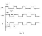
- the applied delayed output clock signal through delay means 16 is applied to the input 52 of inverter 50 and is denoted by a "B", which corresponds to the waveform B of Figure 2 which will be referred to hereinafter.
- AND gate 36 includes an output 37 coupled to set input 22 of latch 12 and NOR gate 38 has an output 39 coupled to the reset input of latch 12.
- the CMOS microprocessor to be clocked by the output clock signal includes a first circuit portion which is active during a first phase of the output clock signal when the output clock signal is at a high level and a second circuit portion which is active during a second phase of the output clock signal when the output clock signal is at a low level.
- Each circuit portion includes a speed path formed by internal gate delays which result in minimum first and second execution times during the first and second phases to enable each circuit portion to complete its execution during its respective output clock signal phase.
- the input clock signal provided by external source 80 sets and resets the latch 62 to cause the latch 62 to provide the output clock signal.
- the input clock signal only sets and resets the latch 62 when the latch is set or reset enabled by the output of the delay means 16.
- the number of inverters 28 selected for delay means 16 should represent a delay time at least equal to the greater of the first and second minimum execution times. By so doing, each phase of the output clock signal will be assumed to provide a sufficient execution time to accommodate the speed paths of both circuit portions.
- the delay time of the delay means 16 assumes a minimum execution time for each phase of the output clock signal.
- the actual duration of each phase may be longer than the minimum execution times required by the processor because the input clock signal may define first or second phases which are longer than the delay time of the delay means 16. If one of the phases defined by the input clock signal is longer than the delay time, the delay means 16 will have no effect because it would have already enabled the latch 62 to be set or reset by the time the input clock signal changes to the next phase.
- the clock generator 10 is also self-regulating.
- the self-regulation comes into play because the delay means is arranged to vary its delay time in direct relation to the delay time represented by the microprocessor speed paths.
- the delay means 16 includes a plurality of serially coupled inverters with each inverter representing a delay proportional to an average gate delay of the microprocessor.
- the same parameters such as processing parameters, temperature, and supply voltage magnitude, for example, which vary the delay time of the speed paths will have the same effect on the delay time of the delay means 16.
- the operation of the clock generator illustrated in Fig. 2 is for a case where the input clock signal 54 results in a 50% duty cycle output clock signal.
- the duty cycle of the input clock signal is skewed so that the first phase, PH1′, is shorter than the second phase, PH2′, and is also shorter than the minimum execution time of the microprocessor during the first phase.
- the delay means 16 provides a delay time D which is sufficient to accommodate the speed paths of both circuit portions. Hence, as will be seen hereinafter, the output clock signal will have first and second phases at least equal D.
- the input clock signal waveform 54 indicates that the input clock signal has a period of T and a duty cycle of thirty-three percent.
- the input clock signal is at a high level and the delayed output clock signal at input 52 of inverter 50 is at a low level to cause the latch 12 to be set and the output to be at a high level.
- the input clock signal goes low but since the output clock signal applied to the input 52 of inverter 50 is delayed by one-half of the period T, the input 52 of inverter 50 is still low so that the output 26 of latch 12 remains unchanged.
- the input 52 of inverter 50 goes high by virtue of the one-half period delay provided by the delay means 16.
- the input clock signal is low and the latch 12 is reset enabled by the input 52 of inverter 50 being high to reset the latch 12 and cause the output 26 to go low.
- the output 26 of latch 12 remains low until time T4 when the input clock signal once again goes high and the input 52 of inverter 50 goes low by virtue of the one-half period delay of the output clock signal.
- the foregoing repeats during each full period of the input clock signal for generating the output clock signal having the first and second phases PH1 and PH2 at the output 26 of latch 12.
- the first and second phases PH1 and PH2 are sufficiently long in duration to accommodate the speed paths of the microprocessor for both phases.
- the output clock signal is buffered by the inverters 30 and 32 for application to the CMOS microprocessor circuitry within which the clock generator 10 is utilized.
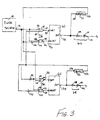
- the clock generator 60 is arranged for providing an output clock signal having a tailored duty cycle with the first phase being unequal to the second phase in duration.
- the clock generator 60 generally includes a first latch 62, a second latch 64, a first buffering means 66, a second buffering means 68, a first delay means 70, a second delay means 72, a first input conditioning circuit 74 and a second input conditioning circuit 76.
- the clock generator 60 is coupled to the output 78 of an external clock source 80 which provides the clock generator 60 with input clock signals.
- the first input conditioning circuit 74 includes an AND gate 82 and a NOR gate 84.
- the AND gate 82 has a first input 86 which is coupled to the output 78 of clock source 80 and a first input 88 of NOR gate 84.
- the output 90 and AND gate 82 is coupled to the set input 92 of latch 62 and the output 94 of NOR gate 84 is coupled to the reset input 96 of latch 62.
- Latch 62 includes an output 98 which is coupled to the input 100 of delay means 70 which in turn has an output 102 coupled to the second input 104 of NOR gate 84 through an-inverter 106.
- the first buffering means 66 which is coupled to the output 98 of latch 62 comprises a pair of serially coupled inverters 108 and 110 which provide at the output 112 of inverter 110 the buffered output clock signal.
- the second input conditioning circuit 76 also includes an AND gate 110 and a NOR gate 112.
- AND gate 110 has a first input 112 which is coupled to the output 78 of the external clock source 80 through an inverter 114.
- AND gate 110 also has a second input 116 which is coupled to the output 102 of the delay means 70.
- NOR gate 112 has a first input 118 which is coupled to the output 78 of the external clock source through the inverter 114. NOR gate 112 also has a second input 120 which is coupled to the output 122 of delay means 72 through an inverter 124.
- AND gate 110 includes an output 126 which is coupled to the set input 128 of the second latch 64.
- NOR gate 112 has an output 130 which is coupled to the reset input 132 of the second latch 64.
- the second latch has an output 134 which is coupled to the input 136 of the delay means 72 and to the second buffering means 68.
- the second buffering means 68 includes a pair of serially coupled inverters 138 and 140 for providing at the output 142 of inverter 140 a buffered second output clock signal which is the inverse of the output clock signal provided at output 112.
- the output 122 of the second delay means 72 is coupled to the second input 87 of AND gate 82.
- the first delay means 70 is coupled between the output 98 of latch 62 and the reset input 96 of the first latch 62 and the set input 78 of the second latch 64.
- the second delay means 72 is coupled between the output 134 of the second latch 64 and the reset input 132 of the second latch 64 and the set input 92 of the first latch 62.
- the delay means 70 and 72 may comprise a different plurality of serially coupled inverters to provided respective different delay times. Hence, each of the delay means 70 and 72 is arranged to delay the first and second phases by a different delay time with the first delay means delaying the first phase and second delay means delaying the second phase.
- the operation of the clock generator 60 is similar to that of the clock generator 10 of Figure 1.
- the main difference is that the second delay means 72 set enables the latch 62 and the first delay means 70 set enables the second latch 64.
- the first latch 62 is reset enabled by the first delay means 70 and the second latch is reset enabled by the second delay means 72.
- each latch once set, is prevented from being cleared until the delay established by its corresponding delay means has passed.
- the resulting output clock signal at output 112 of inverter 110 will thus have a first phase established by the first delay means 70 and a second phase established by the second delay means 72.
- the first and second delay means are preferably a plurality of serially coupled inverters, they will exhibit the same self-regulatory properties previously described. Hence, first and second execution times during the first and second phases of sufficient length to accommodate the first and second speed paths will always be provided.
- the first and second delays 70 and 72 will only be asserted if needed. If the first or second phases of the input clock signal are longer than the first or second delay, the respective delay will already have set enabled the other latch so that the next phase of the input clock signal will pass through. The delays are only asserted if the input clock signal frequency is too high or the duty cycle is skewed to provide a phase which is shorter than one of the delay times.
- phase n is set when both phase n-1 is complete and the input is equal to state n and phase n is reset when both phase n is complete and the input is not equal to state n.
- the present invention provides new and improved clock generators for clocking CMOS microprocessors.
- the clock generators disclosed herein include circuit components which are compatible with CMOS technology and thus, may be readily incorporated into CMOS integrated circuit microprocessor devices.
- the clock generators of Figures 1 and 3 do not require any start-up time and are arranged to provide appropriate cycle clock signals upon being initially powered.
- the clock generators of Figure 1 and 3 do not incorporate phase-locked loops which, as previously mentioned, have required a start-up time and have been relatively expensive to implement in integrated circuit devices, such as, CMOS integrated circuit microprocessor devices.
Landscapes
- Engineering & Computer Science (AREA)
- Theoretical Computer Science (AREA)
- Physics & Mathematics (AREA)
- General Engineering & Computer Science (AREA)
- General Physics & Mathematics (AREA)
- Oscillators With Electromechanical Resonators (AREA)
- Control Of Motors That Do Not Use Commutators (AREA)
- Stabilization Of Oscillater, Synchronisation, Frequency Synthesizers (AREA)
- Manipulation Of Pulses (AREA)
- Pulse Circuits (AREA)
Applications Claiming Priority (2)
| Application Number | Priority Date | Filing Date | Title |
|---|---|---|---|
| US532311 | 1990-06-01 | ||
| US07/532,311 US5059818A (en) | 1990-06-01 | 1990-06-01 | Self-regulating clock generator |
Publications (3)
| Publication Number | Publication Date |
|---|---|
| EP0459696A2 true EP0459696A2 (de) | 1991-12-04 |
| EP0459696A3 EP0459696A3 (en) | 1994-06-15 |
| EP0459696B1 EP0459696B1 (de) | 1998-09-09 |
Family
ID=24121249
Family Applications (1)
| Application Number | Title | Priority Date | Filing Date |
|---|---|---|---|
| EP91304635A Expired - Lifetime EP0459696B1 (de) | 1990-06-01 | 1991-05-22 | Selbstregulierender Taktgenerator |
Country Status (5)
| Country | Link |
|---|---|
| US (1) | US5059818A (de) |
| EP (1) | EP0459696B1 (de) |
| JP (1) | JPH04232519A (de) |
| AT (1) | ATE170994T1 (de) |
| DE (1) | DE69130134T2 (de) |
Cited By (6)
| Publication number | Priority date | Publication date | Assignee | Title |
|---|---|---|---|---|
| EP0602422A1 (de) * | 1992-12-15 | 1994-06-22 | International Business Machines Corporation | Dynamische Frequenzversetzung mit einem durch eins teilenden Taktgenerator |
| EP0608972A1 (de) * | 1993-01-29 | 1994-08-03 | Advanced Micro Devices, Inc. | Digitaler Taktgenerator |
| EP0604126A3 (de) * | 1992-12-22 | 1997-02-05 | Motorola Inc | Konditionsschaltung für ein Taktsignal. |
| DE19924343A1 (de) * | 1999-05-27 | 2000-11-23 | Siemens Ag | Programmgesteuerte Einheit |
| WO2016190956A1 (en) * | 2015-05-22 | 2016-12-01 | Qualcomm Incorporated | Area-efficient metal-programmable pulse latch design |
| US9979394B2 (en) | 2016-02-16 | 2018-05-22 | Qualcomm Incorporated | Pulse-generator |
Families Citing this family (44)
| Publication number | Priority date | Publication date | Assignee | Title |
|---|---|---|---|---|
| EP0429850B1 (de) * | 1989-11-29 | 1995-08-16 | Siemens Aktiengesellschaft | Schaltungsanordnung zur Taktregenerierung in taktgesteuerten Informationsverarbeitungsanlagen |
| JP2639207B2 (ja) * | 1989-12-08 | 1997-08-06 | 日本電気株式会社 | 出力回路 |
| US5291070A (en) * | 1991-01-28 | 1994-03-01 | Advanced Micro Devices, Inc. | Microprocessor synchronous timing system |
| ATE295571T1 (de) * | 1991-03-01 | 2005-05-15 | Advanced Micro Devices Inc | Ausgangspuffer für mikroprozessor |
| US5278456A (en) * | 1991-06-24 | 1994-01-11 | International Business Machines Corporation | Process independent digital clock signal shaping network |
| US5307381A (en) * | 1991-12-27 | 1994-04-26 | Intel Corporation | Skew-free clock signal distribution network in a microprocessor |
| US5566129A (en) * | 1992-02-28 | 1996-10-15 | Sony Corporation | Semiconductor memory device with address transition detector |
| US5319678A (en) * | 1992-03-20 | 1994-06-07 | Digital Equipment Corporation | Clocking system for asynchronous operations |
| US5359232A (en) * | 1992-05-08 | 1994-10-25 | Cyrix Corporation | Clock multiplication circuit and method |
| KR940012823A (ko) * | 1992-11-18 | 1994-06-24 | 사토 후미오 | 클록신호 생성회로 |
| US5450574A (en) * | 1993-03-29 | 1995-09-12 | All Computers Inc. | Apparatus and method for enhancing the performance of personal computers |
| GB9411602D0 (en) * | 1994-06-09 | 1994-08-03 | Inmos Ltd | Pulse generation |
| US5583461A (en) * | 1994-09-19 | 1996-12-10 | Advanced Micro Devices, Inc. | Internal clock signal generation circuit having external clock detection and a selectable internal clock pulse |
| US5721695A (en) * | 1994-10-17 | 1998-02-24 | Advanced Micro Devices, Inc. | Simulation by emulating level sensitive latches with edge trigger latches |
| US5572719A (en) * | 1994-11-22 | 1996-11-05 | Advanced Micro Devices | Clock control system for microprocessors including a delay sensing circuit |
| KR960019978A (ko) * | 1994-11-23 | 1996-06-17 | 문정환 | 펄스 발생기 |
| US5539337A (en) * | 1994-12-30 | 1996-07-23 | Intel Corporation | Clock noise filter for integrated circuits |
| US5557225A (en) * | 1994-12-30 | 1996-09-17 | Intel Corporation | Pulsed flip-flop circuit |
| JPH08195654A (ja) * | 1995-01-17 | 1996-07-30 | Ando Electric Co Ltd | クロック再生回路 |
| US5672991A (en) * | 1995-04-14 | 1997-09-30 | International Business Machines Corporation | Differential delay line circuit for outputting signal with equal pulse widths |
| US5633607A (en) * | 1995-04-28 | 1997-05-27 | Mosaid Technologies Incorporated | Edge triggered set-reset flip-flop (SRFF) |
| DE69530288D1 (de) * | 1995-05-31 | 2003-05-15 | St Microelectronics Srl | Impulsgenerator, Schaltung und Verfahren zur Ansteuerung von elektronischen Vorrichtungen und deren Verwendung |
| US6229861B1 (en) * | 1995-06-07 | 2001-05-08 | Intel Corporation | Clock distribution network utilizing local deskewing clock generator circuitry |
| US5614845A (en) * | 1995-09-08 | 1997-03-25 | International Business Machines Corporation | Independent clock edge regulation |
| JP3375504B2 (ja) * | 1996-12-17 | 2003-02-10 | 富士通株式会社 | パルス発生回路および半導体記憶装置 |
| US5920222A (en) * | 1997-04-22 | 1999-07-06 | International Business Machines Corporation | Tunable pulse generator based on a wave pipeline |
| US6154076A (en) * | 1997-09-19 | 2000-11-28 | Texas Instruments Incorporated | Phase alignment circuit for periodic signals |
| US5977809A (en) * | 1997-11-12 | 1999-11-02 | Taiwan Semiconductor Manufacturing Co., Ltd. | Programmable non-overlap clock generator |
| US6023182A (en) * | 1997-12-31 | 2000-02-08 | Intel Corporation | High gain pulse generator circuit with clock gating |
| JP3678570B2 (ja) * | 1998-01-17 | 2005-08-03 | 日本電気株式会社 | 半導体集積回路 |
| US5929684A (en) * | 1998-03-06 | 1999-07-27 | Siemens Aktiengesellschaft | Feedback pulse generators |
| FR2783649B1 (fr) * | 1998-09-17 | 2000-11-17 | St Microelectronics Sa | Circuit de filtrage d'un signal d'horloge |
| DE10000758C2 (de) * | 2000-01-11 | 2001-11-15 | Infineon Technologies Ag | Impulserzeuger |
| TW531964B (en) * | 2001-12-31 | 2003-05-11 | Winbond Electronics Corp | Frequency signal starting apparatus and its method |
| KR100454126B1 (ko) * | 2002-01-15 | 2004-10-26 | 삼성전자주식회사 | 분리된 클록 라인을 구비한 정보 처리 시스템 |
| US6992517B2 (en) * | 2003-08-11 | 2006-01-31 | Atmel Corporation | Self-limiting pulse width modulation regulator |
| US7408420B2 (en) * | 2005-09-27 | 2008-08-05 | Intel Corporation | Multi mode clock generator |
| US7317343B1 (en) * | 2005-10-25 | 2008-01-08 | Lattice Semiconductor Corporation | Pulse-generation circuit with multi-delay block and set-reset latches |
| KR100829453B1 (ko) | 2006-08-11 | 2008-05-15 | 주식회사 하이닉스반도체 | Dll 회로의 기준 클럭 생성 장치 및 방법 |
| US7667500B1 (en) * | 2006-11-14 | 2010-02-23 | Xilinx, Inc. | Glitch-suppressor circuits and methods |
| CN103297009B (zh) * | 2013-06-24 | 2016-02-17 | 成都鸿芯纪元科技有限公司 | 一种fpga上电复位系统 |
| US10389335B1 (en) * | 2018-05-04 | 2019-08-20 | Apple Inc. | Clock pulse generation circuit |
| GB202306557D0 (en) * | 2023-05-03 | 2023-06-14 | Nordic Semiconductor Asa | Glitch filter |
| CN121586996A (zh) * | 2023-06-14 | 2026-02-27 | 华为技术有限公司 | 时钟发生器系统和方法 |
Family Cites Families (6)
| Publication number | Priority date | Publication date | Assignee | Title |
|---|---|---|---|---|
| US3454884A (en) * | 1966-11-01 | 1969-07-08 | Xerox Corp | Duty cycle control circuit |
| US4794281A (en) * | 1986-01-24 | 1988-12-27 | National Semiconductor Corporation | Speed-up circuit for transistor logic output device |
| US4691124A (en) * | 1986-05-16 | 1987-09-01 | Motorola, Inc. | Self-compensating, maximum speed integrated circuit |
| US4968907A (en) * | 1987-11-19 | 1990-11-06 | Eg&G Instruements, Inc. | Digital delay generator |
| JPH01144719A (ja) * | 1987-11-30 | 1989-06-07 | Toshiba Corp | リトリガブル・マルチバイブレータ |
| US4985639A (en) * | 1989-07-07 | 1991-01-15 | Hewlett-Packard Company | Logic edge timing generation |
-
1990
- 1990-06-01 US US07/532,311 patent/US5059818A/en not_active Expired - Fee Related
-
1991
- 1991-05-22 AT AT91304635T patent/ATE170994T1/de not_active IP Right Cessation
- 1991-05-22 EP EP91304635A patent/EP0459696B1/de not_active Expired - Lifetime
- 1991-05-22 DE DE69130134T patent/DE69130134T2/de not_active Expired - Fee Related
- 1991-05-31 JP JP3129758A patent/JPH04232519A/ja not_active Withdrawn
Cited By (7)
| Publication number | Priority date | Publication date | Assignee | Title |
|---|---|---|---|---|
| EP0602422A1 (de) * | 1992-12-15 | 1994-06-22 | International Business Machines Corporation | Dynamische Frequenzversetzung mit einem durch eins teilenden Taktgenerator |
| EP0604126A3 (de) * | 1992-12-22 | 1997-02-05 | Motorola Inc | Konditionsschaltung für ein Taktsignal. |
| EP0608972A1 (de) * | 1993-01-29 | 1994-08-03 | Advanced Micro Devices, Inc. | Digitaler Taktgenerator |
| DE19924343A1 (de) * | 1999-05-27 | 2000-11-23 | Siemens Ag | Programmgesteuerte Einheit |
| WO2016190956A1 (en) * | 2015-05-22 | 2016-12-01 | Qualcomm Incorporated | Area-efficient metal-programmable pulse latch design |
| US9564881B2 (en) | 2015-05-22 | 2017-02-07 | Qualcomm Incorporated | Area-efficient metal-programmable pulse latch design |
| US9979394B2 (en) | 2016-02-16 | 2018-05-22 | Qualcomm Incorporated | Pulse-generator |
Also Published As
| Publication number | Publication date |
|---|---|
| EP0459696A3 (en) | 1994-06-15 |
| ATE170994T1 (de) | 1998-09-15 |
| US5059818A (en) | 1991-10-22 |
| EP0459696B1 (de) | 1998-09-09 |
| JPH04232519A (ja) | 1992-08-20 |
| DE69130134D1 (de) | 1998-10-15 |
| DE69130134T2 (de) | 1999-05-06 |
Similar Documents
| Publication | Publication Date | Title |
|---|---|---|
| EP0459696B1 (de) | Selbstregulierender Taktgenerator | |
| US5359232A (en) | Clock multiplication circuit and method | |
| JP3560997B2 (ja) | マイクロプロセッサ回路 | |
| US6882196B2 (en) | Duty cycle corrector | |
| US6064247A (en) | Multiple frequency clock generation and synchronization | |
| JPH01149516A (ja) | クロック発生装置 | |
| US20020053931A1 (en) | Phase difference signal generator and multi-phase clock signal generator having phase interpolator | |
| US6049236A (en) | Divide-by-one or divide-by-two qualified clock driver with glitch-free transitions between operating frequencies | |
| US6535048B1 (en) | Secure asynchronous clock multiplexer | |
| JPH04339410A (ja) | 周波数逓倍回路 | |
| GB2273834A (en) | Clock signal conditioning circuit | |
| US6329861B1 (en) | Clock generator circuit | |
| US6271702B1 (en) | Clock circuit for generating a delay | |
| US6661262B1 (en) | Frequency doubling two-phase clock generation circuit | |
| US5617563A (en) | Duty cycle independent tunable clock | |
| JPH11110068A (ja) | 半導体装置 | |
| JPH10215153A (ja) | クロック逓倍回路及び半導体集積回路 | |
| JP3240713B2 (ja) | 多相クロック生成回路 | |
| US6642756B1 (en) | Frequency multiplier design | |
| JPH05100763A (ja) | クロツク制御回路 | |
| JPH0362611A (ja) | クロック発生回路 | |
| JP2705174B2 (ja) | 発振回路 | |
| JP3011047B2 (ja) | 位相比較回路 | |
| KR100457331B1 (ko) | 펄스발생회로 | |
| JPH04183017A (ja) | フリップフロップ回路 |
Legal Events
| Date | Code | Title | Description |
|---|---|---|---|
| PUAI | Public reference made under article 153(3) epc to a published international application that has entered the european phase |
Free format text: ORIGINAL CODE: 0009012 |
|
| AK | Designated contracting states |
Kind code of ref document: A2 Designated state(s): AT BE CH DE DK ES FR GB GR IT LI LU NL SE |
|
| PUAL | Search report despatched |
Free format text: ORIGINAL CODE: 0009013 |
|
| AK | Designated contracting states |
Kind code of ref document: A3 Designated state(s): AT BE CH DE DK ES FR GB GR IT LI LU NL SE |
|
| 17P | Request for examination filed |
Effective date: 19941128 |
|
| 17Q | First examination report despatched |
Effective date: 19970704 |
|
| GRAG | Despatch of communication of intention to grant |
Free format text: ORIGINAL CODE: EPIDOS AGRA |
|
| GRAG | Despatch of communication of intention to grant |
Free format text: ORIGINAL CODE: EPIDOS AGRA |
|
| GRAH | Despatch of communication of intention to grant a patent |
Free format text: ORIGINAL CODE: EPIDOS IGRA |
|
| GRAH | Despatch of communication of intention to grant a patent |
Free format text: ORIGINAL CODE: EPIDOS IGRA |
|
| GRAA | (expected) grant |
Free format text: ORIGINAL CODE: 0009210 |
|
| AK | Designated contracting states |
Kind code of ref document: B1 Designated state(s): AT BE CH DE DK ES FR GB GR IT LI LU NL SE |
|
| PG25 | Lapsed in a contracting state [announced via postgrant information from national office to epo] |
Ref country code: IT Free format text: LAPSE BECAUSE OF FAILURE TO SUBMIT A TRANSLATION OF THE DESCRIPTION OR TO PAY THE FEE WITHIN THE PRE;WARNING: LAPSES OF ITALIAN PATENTS WITH EFFECTIVE DATE BEFORE 2007 MAY HAVE OCCURRED AT ANY TIME BEFORE 2007. THE CORRECT EFFECTIVE DATE MAY BE DIFFERENT FROM THE ONE RECORDED.SCRIBED TIME-LIMIT Effective date: 19980909 Ref country code: NL Free format text: LAPSE BECAUSE OF FAILURE TO SUBMIT A TRANSLATION OF THE DESCRIPTION OR TO PAY THE FEE WITHIN THE PRESCRIBED TIME-LIMIT Effective date: 19980909 Ref country code: LI Free format text: LAPSE BECAUSE OF FAILURE TO SUBMIT A TRANSLATION OF THE DESCRIPTION OR TO PAY THE FEE WITHIN THE PRESCRIBED TIME-LIMIT Effective date: 19980909 Ref country code: GR Free format text: LAPSE BECAUSE OF NON-PAYMENT OF DUE FEES Effective date: 19980909 Ref country code: BE Free format text: LAPSE BECAUSE OF FAILURE TO SUBMIT A TRANSLATION OF THE DESCRIPTION OR TO PAY THE FEE WITHIN THE PRESCRIBED TIME-LIMIT Effective date: 19980909 Ref country code: CH Free format text: LAPSE BECAUSE OF FAILURE TO SUBMIT A TRANSLATION OF THE DESCRIPTION OR TO PAY THE FEE WITHIN THE PRESCRIBED TIME-LIMIT Effective date: 19980909 Ref country code: AT Free format text: LAPSE BECAUSE OF FAILURE TO SUBMIT A TRANSLATION OF THE DESCRIPTION OR TO PAY THE FEE WITHIN THE PRESCRIBED TIME-LIMIT Effective date: 19980909 Ref country code: ES Free format text: THE PATENT HAS BEEN ANNULLED BY A DECISION OF A NATIONAL AUTHORITY Effective date: 19980909 Ref country code: FR Free format text: LAPSE BECAUSE OF FAILURE TO SUBMIT A TRANSLATION OF THE DESCRIPTION OR TO PAY THE FEE WITHIN THE PRESCRIBED TIME-LIMIT Effective date: 19980909 |
|
| REF | Corresponds to: |
Ref document number: 170994 Country of ref document: AT Date of ref document: 19980915 Kind code of ref document: T |
|
| REG | Reference to a national code |
Ref country code: CH Ref legal event code: EP |
|
| REF | Corresponds to: |
Ref document number: 69130134 Country of ref document: DE Date of ref document: 19981015 |
|
| PG25 | Lapsed in a contracting state [announced via postgrant information from national office to epo] |
Ref country code: SE Free format text: LAPSE BECAUSE OF FAILURE TO SUBMIT A TRANSLATION OF THE DESCRIPTION OR TO PAY THE FEE WITHIN THE PRESCRIBED TIME-LIMIT Effective date: 19981209 Ref country code: DK Free format text: LAPSE BECAUSE OF FAILURE TO SUBMIT A TRANSLATION OF THE DESCRIPTION OR TO PAY THE FEE WITHIN THE PRESCRIBED TIME-LIMIT Effective date: 19981209 |
|
| NLV1 | Nl: lapsed or annulled due to failure to fulfill the requirements of art. 29p and 29m of the patents act | ||
| EN | Fr: translation not filed | ||
| REG | Reference to a national code |
Ref country code: CH Ref legal event code: PL |
|
| PG25 | Lapsed in a contracting state [announced via postgrant information from national office to epo] |
Ref country code: LU Free format text: LAPSE BECAUSE OF NON-PAYMENT OF DUE FEES Effective date: 19990522 |
|
| PLBE | No opposition filed within time limit |
Free format text: ORIGINAL CODE: 0009261 |
|
| STAA | Information on the status of an ep patent application or granted ep patent |
Free format text: STATUS: NO OPPOSITION FILED WITHIN TIME LIMIT |
|
| 26N | No opposition filed | ||
| REG | Reference to a national code |
Ref country code: GB Ref legal event code: IF02 |
|
| PGFP | Annual fee paid to national office [announced via postgrant information from national office to epo] |
Ref country code: GB Payment date: 20020404 Year of fee payment: 12 |
|
| PGFP | Annual fee paid to national office [announced via postgrant information from national office to epo] |
Ref country code: DE Payment date: 20020531 Year of fee payment: 12 |
|
| PG25 | Lapsed in a contracting state [announced via postgrant information from national office to epo] |
Ref country code: GB Free format text: LAPSE BECAUSE OF NON-PAYMENT OF DUE FEES Effective date: 20030522 |
|
| PG25 | Lapsed in a contracting state [announced via postgrant information from national office to epo] |
Ref country code: DE Free format text: LAPSE BECAUSE OF NON-PAYMENT OF DUE FEES Effective date: 20031202 |
|
| GBPC | Gb: european patent ceased through non-payment of renewal fee |
Effective date: 20030522 |