EP0459252A2 - Herstellungsverfahren für ein Dünnschichtmuster mit trapezförmigem Querschnitt - Google Patents
Herstellungsverfahren für ein Dünnschichtmuster mit trapezförmigem Querschnitt Download PDFInfo
- Publication number
- EP0459252A2 EP0459252A2 EP91108046A EP91108046A EP0459252A2 EP 0459252 A2 EP0459252 A2 EP 0459252A2 EP 91108046 A EP91108046 A EP 91108046A EP 91108046 A EP91108046 A EP 91108046A EP 0459252 A2 EP0459252 A2 EP 0459252A2
- Authority
- EP
- European Patent Office
- Prior art keywords
- thin film
- pattern
- resist
- photo
- forming
- Prior art date
- Legal status (The legal status is an assumption and is not a legal conclusion. Google has not performed a legal analysis and makes no representation as to the accuracy of the status listed.)
- Granted
Links
Images


Classifications
-
- H—ELECTRICITY
- H10—SEMICONDUCTOR DEVICES; ELECTRIC SOLID-STATE DEVICES NOT OTHERWISE PROVIDED FOR
- H10D—INORGANIC ELECTRIC SEMICONDUCTOR DEVICES
- H10D1/00—Resistors, capacitors or inductors
- H10D1/40—Resistors
- H10D1/47—Resistors having no potential barriers
-
- G—PHYSICS
- G03—PHOTOGRAPHY; CINEMATOGRAPHY; ANALOGOUS TECHNIQUES USING WAVES OTHER THAN OPTICAL WAVES; ELECTROGRAPHY; HOLOGRAPHY
- G03F—PHOTOMECHANICAL PRODUCTION OF TEXTURED OR PATTERNED SURFACES, e.g. FOR PRINTING, FOR PROCESSING OF SEMICONDUCTOR DEVICES; MATERIALS THEREFOR; ORIGINALS THEREFOR; APPARATUS SPECIALLY ADAPTED THEREFOR
- G03F7/00—Photomechanical, e.g. photolithographic, production of textured or patterned surfaces, e.g. printing surfaces; Materials therefor, e.g. comprising photoresists; Apparatus specially adapted therefor
- G03F7/20—Exposure; Apparatus therefor
- G03F7/2022—Multi-step exposure, e.g. hybrid; backside exposure; blanket exposure, e.g. for image reversal; edge exposure, e.g. for edge bead removal; corrective exposure
-
- G—PHYSICS
- G03—PHOTOGRAPHY; CINEMATOGRAPHY; ANALOGOUS TECHNIQUES USING WAVES OTHER THAN OPTICAL WAVES; ELECTROGRAPHY; HOLOGRAPHY
- G03F—PHOTOMECHANICAL PRODUCTION OF TEXTURED OR PATTERNED SURFACES, e.g. FOR PRINTING, FOR PROCESSING OF SEMICONDUCTOR DEVICES; MATERIALS THEREFOR; ORIGINALS THEREFOR; APPARATUS SPECIALLY ADAPTED THEREFOR
- G03F7/00—Photomechanical, e.g. photolithographic, production of textured or patterned surfaces, e.g. printing surfaces; Materials therefor, e.g. comprising photoresists; Apparatus specially adapted therefor
- G03F7/26—Processing photosensitive materials; Apparatus therefor
- G03F7/38—Treatment before imagewise removal, e.g. prebaking
-
- H—ELECTRICITY
- H10—SEMICONDUCTOR DEVICES; ELECTRIC SOLID-STATE DEVICES NOT OTHERWISE PROVIDED FOR
- H10D—INORGANIC ELECTRIC SEMICONDUCTOR DEVICES
- H10D64/00—Electrodes of devices having potential barriers
- H10D64/01—Manufacture or treatment
- H10D64/013—Manufacture or treatment of electrodes having a conductor capacitively coupled to a semiconductor by an insulator
- H10D64/01302—Manufacture or treatment of electrodes having a conductor capacitively coupled to a semiconductor by an insulator the insulator being formed after the semiconductor body, the semiconductor being silicon
- H10D64/01304—Manufacture or treatment of electrodes having a conductor capacitively coupled to a semiconductor by an insulator the insulator being formed after the semiconductor body, the semiconductor being silicon characterised by the conductor
- H10D64/01324—Manufacture or treatment of electrodes having a conductor capacitively coupled to a semiconductor by an insulator the insulator being formed after the semiconductor body, the semiconductor being silicon characterised by the conductor characterised by the sectional shape, e.g. T or inverted-T
-
- H—ELECTRICITY
- H10—SEMICONDUCTOR DEVICES; ELECTRIC SOLID-STATE DEVICES NOT OTHERWISE PROVIDED FOR
- H10P—GENERIC PROCESSES OR APPARATUS FOR THE MANUFACTURE OR TREATMENT OF DEVICES COVERED BY CLASS H10
- H10P50/00—Etching of wafers, substrates or parts of devices
- H10P50/20—Dry etching; Plasma etching; Reactive-ion etching
- H10P50/26—Dry etching; Plasma etching; Reactive-ion etching of conductive or resistive materials
- H10P50/264—Dry etching; Plasma etching; Reactive-ion etching of conductive or resistive materials by chemical means
- H10P50/266—Dry etching; Plasma etching; Reactive-ion etching of conductive or resistive materials by chemical means by vapour etching only
-
- H—ELECTRICITY
- H10—SEMICONDUCTOR DEVICES; ELECTRIC SOLID-STATE DEVICES NOT OTHERWISE PROVIDED FOR
- H10P—GENERIC PROCESSES OR APPARATUS FOR THE MANUFACTURE OR TREATMENT OF DEVICES COVERED BY CLASS H10
- H10P50/00—Etching of wafers, substrates or parts of devices
- H10P50/71—Etching of wafers, substrates or parts of devices using masks for conductive or resistive materials
-
- H—ELECTRICITY
- H10—SEMICONDUCTOR DEVICES; ELECTRIC SOLID-STATE DEVICES NOT OTHERWISE PROVIDED FOR
- H10P—GENERIC PROCESSES OR APPARATUS FOR THE MANUFACTURE OR TREATMENT OF DEVICES COVERED BY CLASS H10
- H10P50/00—Etching of wafers, substrates or parts of devices
- H10P50/73—Etching of wafers, substrates or parts of devices using masks for insulating materials
-
- H—ELECTRICITY
- H10—SEMICONDUCTOR DEVICES; ELECTRIC SOLID-STATE DEVICES NOT OTHERWISE PROVIDED FOR
- H10P—GENERIC PROCESSES OR APPARATUS FOR THE MANUFACTURE OR TREATMENT OF DEVICES COVERED BY CLASS H10
- H10P76/00—Manufacture or treatment of masks on semiconductor bodies, e.g. by lithography or photolithography
- H10P76/20—Manufacture or treatment of masks on semiconductor bodies, e.g. by lithography or photolithography of masks comprising organic materials
- H10P76/204—Manufacture or treatment of masks on semiconductor bodies, e.g. by lithography or photolithography of masks comprising organic materials of organic photoresist masks
- H10P76/2041—Photolithographic processes
-
- H—ELECTRICITY
- H10—SEMICONDUCTOR DEVICES; ELECTRIC SOLID-STATE DEVICES NOT OTHERWISE PROVIDED FOR
- H10P—GENERIC PROCESSES OR APPARATUS FOR THE MANUFACTURE OR TREATMENT OF DEVICES COVERED BY CLASS H10
- H10P76/00—Manufacture or treatment of masks on semiconductor bodies, e.g. by lithography or photolithography
- H10P76/40—Manufacture or treatment of masks on semiconductor bodies, e.g. by lithography or photolithography of masks comprising inorganic materials
Definitions
- the present invention relates generally to a method of forming a semiconductor device, and more particularly to a method of performing a photoetching process selectively on such thin films as a polysilicon film, an insulating film and a metallic film.
- the dry etching technique is generally classified into isotropic etching such as CDE (Chemical Dry Etching) and anisotropic etching such as RIE (Reactive Ion Etching).
- CDE Chemical Dry Etching
- RIE Reactive Ion Etching
- a side face of a thin film pattern is formed substantially vertical to a substrate.
- the new thin film has a difference between film thickness t1 at its flat area and film thickness t2 at its side area.
- the relationship between t1 and t2 is: t1 ⁇ t2
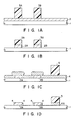
- Figs. 1A to 1D are cross-sectional views illustrating the steps of a process for fabricating a conventional semiconductor device.
- a first polysilicon layer 2 which is undoped or has a low impurity concentration, is formed on a base layer 1 (a silicon substrate or a silicon oxide film).
- a photoresist is coated over the first polysilicon layer 2. The photoresist is selectively etched by means of photoetching, thus obtaining a photoresist pattern 3B.
- the polysilicon layer 2 is selectively etched by means of RIE (one of isotropic etching techniques), using the photoresist pattern 3B as a mask.
- RIE one of isotropic etching techniques
- a second polysilicon layer 4 having a high impurity concentration is formed over the base layer 1 and polysilicon patterns 2A and 2B.
- a photoresist is coated over the second polysilicon layer 4, and the photoresist is selectively etched by means of photoetching, thereby obtaining a photoresist pattern 5.
- the second polysilicon layer 4 is selectively etched by means of RIE and a polysilicon pattern 4A is obtained.
- the second polysilicon 4 is left on the side walls of the polysilicon patterns 2A and 2B.
- the impurity concentration of the polysilicon patterns 2A and 2B varies.
- the resistance values of the resistors vary and the characteristic of the integrated circuit changes.
- the second polysilicon layer 2 on the side walls of the polysilicon patterns 2A and 2B are entirely removed.
- the base layer 1 is over-etched and is damaged by RIE.
- the reliability of the semiconductor device is deteriorated.
- the present invention has been made in consideration of the above circumstances, and an object of the invention is to provide a method of fabricating a semiconductor device wherein no portion of a new thin film is left on the side wall of a thin film pattern formed by isotropic etching.
- Another object of the invention is to provide a method of forming a thin film pattern with a trapezoidal cross section.
- a method of forming a thin film pattern comprising the steps of: forming a thin film on a major surface of a substrate; forming a resist pattern, which has an inverted-trapezoidal cross section, on the thin film; and dry-etching the thin film selectively, with the resist pattern having the inverted-trapezoidal cross section employed as a mask, thereby forming a thin film pattern.
- the thin film pattern has a trapezoidal cross section, it is possible that a new thin film formed on the thin film pattern has a uniform thickness. Thus, even if a new thin film is formed by isotropic etching, no portion of the new thin film is left on the side wall of the thin film pattern.
- Figs. 2A to 2F are cross-sectional views illustrating the steps of a process for fabricating a semiconductor device according to a first embodiment.
- a first polysilicon layer 2 which is undoped or has a low impurity concentration, is formed on a base layer 1 (e.g. silicon oxide film or a silicon substrate).
- a positive type photoresist is coated on the polysilicon layer 2.
- the photoresist is selectively etched by means of photoetching.
- an image reverse method is employed. The image reverse method will be described in detail in connection with the second and third embodiments.
- the angle ⁇ 1 defined by the upper surface of the first polysilicon layer 2 and each side wall of the resist patterns 3A and 3B is acute and less than 90°.
- Each of the resist patterns 3A and 3B has an inverted-trapezoidal cross section.
- the first polysilicon layer 2 is selectively etched by means of dry etching (e.g., RIE).
- dry etching e.g., RIE
- the angle ⁇ 2 defined by the upper surface of the base layer 1 and each side wall of the silicon patterns 2A and 2B is obtuse and more than 90°.
- Each of polysilicon patterns 2A and 2B has a trapezoidal cross section.
- the patterns 2A and 2B constitute, for example, resistors of an integrated circuit.
- a second polysilicon layer 4 having a high impurity concentration is formed over the base layer 1 and polysilicon patterns 2A and 2B.
- the thickness of the second polysilicon layer 4 is uniform.
- each of polysilicon patterns 2A and 2B is trapezoidal and the side wall thereof is inclined.
- a photoresist is coated on the second polysilicon layer 4, and the photoresist is selectively etched by means of conventional photoetching, thereby obtaining a photoresist pattern 5.
- the second polysilicon layer 4 is selectively etched by means of isotropic etching (e.g. RIE). Thus, the second polysilicon layer 4 is completely removed, without being left on the side walls of the polysilicon patterns 2A and 2B, and without over-etching.
- a polysilicon pattern 5 is obtained at the region masked by the photoresist pattern 5.
- the polysilicon pattern 5 constitutes, for example, a wiring layer in an integrated circuit or a gate electrode of a transistor.
- a thin film pattern having a trapezoidal cross section can be formed, and a new thin film having a uniform thickness can be formed on this thin film pattern.
- Figs. 3A to 3F are cross-sectional views illustrating the steps of a process for fabricating a semiconductor device according to the second embodiment.
- a first polysilicon layer 2 is formed on a substrate 1.
- a positive type photoresist 102 with a thickness of about 1.0 ⁇ m to 2.0 ⁇ m is coated on the polysilicon layer 2. Then, a prebaking process is carried out.
- the base polymer is, for example, phenol novolak resin, and diazo naphtho-quinone.
- the photoresist 102 contains, for example, azo dye.
- the positive type photoresist 102 is selectively irradiated with ultraviolet 104, with a reticle employed as a mask, as shown in Fig. 3B.
- the condition for the selective exposure is that, for example, a g-ray (wavelength: 436 nm; g-ray is generally called "ultraviolet") is used and the quantity of ultraviolet is 300 mJ/cm2.
- the photoresist 102 is subjected to selective exposure, and a selectively photo-sensitized region 102a is obtained. Alkali-soluble indene carboxylic acid is produced in the photo-sensitized region 102a.
- the substrate 1 coated with photoresist 102 is put in heat-treatment furnace 105.
- the substrate 1 is heated in an ammonia gas atmosphere 106.
- the heat treatment is performed at a temperature of 95 to 120°C for 75 minutes.
- the indene carboxylic acid is crosslinked and alkali-insoluble indene is produced.
- This step is called an image reverse heat treatment step.
- the entire surface of the photoresist 102 is irradiated with ultraviolet 107, thus effecting total surface exposure.
- ultraviolet wavelength: 200 to 450 nm
- Non-sensitized region 102b of the photoresist 102 is newly sensitized by the total surface exposure, and alkali-soluble indene carboxylic acid is produced.
- the substrate 1 is immersed in an alkali water solution, and the photoresist 102 is developed. Consequently, the region 102b where indene carboxylic acid is produced is removed and the region 102a where indene is produced remains.
- the region 102a sensitized in the selective exposure step (first exposure) described with reference to Fig. 2B is left, and the image is reversed, compared to the normal positive type resist. This type of photoetching is called an image reverse method.
- an acute angle ⁇ 1 is defined by the side wall of the pattern 102a and the upper surface of the polysilicon layer 2.
- the photoresist pattern 102a has an inverted-trapezoidal cross section.
- isotropic etching e.g. RIE
- RIE isotropic etching
- an azo dye is contained in the photoresist 102. Since the photoresist 102 contains the azo dye, the ultraviolet transmissivity decreases, and the quantity of ultraviolet reaching the deepest part of the photoresist 102 decreases. Where the quantity of light reaching the deepest part decreases, the sensitized part 102 is tapered. By changing the quantity of dye in the photoresist 102, the degree of tapering of the sensitized part 102a varies. In other words, the angle ⁇ 1 of the inclined side wall of the photoresist pattern 102a varies. For example, if a large quantity of dye is contained in the resist 102 and the image reverse method is carried out, the angle ⁇ 1 is shifted from 90° towards 0°. If the quantity of dye is small, the angle ⁇ 1 approaches 90°.
- the angle ⁇ 2 of the side wall of the polysilicon pattern 2a obtained by the method of the present invention also varies. Taking advantage of this phenomenon, the angle ⁇ 2 of the side wall of the polysilicon pattern 2a can be controlled. For example, if the angle ⁇ 1 approaches 90°, the angle ⁇ 2 also approaches 90°. If the angle ⁇ 1 approaches 0°, the angle ⁇ 2 also approaches 180°.
- the inclination angle ⁇ 2 of the side wall of the polysilicon pattern 2a can be varied by altering the quantity of dye contained in the photoresist 102.
- the thin film pattern 2a can have a wide margin.
- the method of controlling the cross sectional shape of the resist pattern is not limited to the changing of dye quantity in the photoresist 102; the quantity of ultraviolet 104 may be altered in the selective exposure process illustrated in Fig. 3B.
- the inclination angle ⁇ 1 is controlled, as stated above; thus, the inclination angle ⁇ 2 of the side wall of the thin film pattern can be controlled.
- Figs. 4A to 4F are cross-sectional views illustrating the steps of a process for fabricating a semiconductor device according to the third embodiment.
- a polysilicon layer 2 is formed on a substrate 1.
- An image reverse resist 202 is coated on the polysilicon layer 2.
- An example of the image reverse resist 202 is AZ5214E (HOECHST JAPAN Corp.). After the image reverse resist 202 is coated, prebaking is carried out.
- the photoresist 202 is selectively exposed by a method similar to that illustrated in Fig. 3B, thus obtaining a photosensitized region 202a.
- the condition for selective exposure is the use of g-rays in a quantity of 500 mJ/cm2.
- the substrate 1 is placed on the hot plate 205, and the substrate 1 is heated to reverse an image.
- the heat treatment is performed under the condition that the temperature is 95 to 120°C and the time is 1 to 5 minutes. By the heat treatment, alkali insoluble indene is produced in the sensitized region 202a.
- the image reverse resist is used as photoresist; thus, the heat treatment may not be carried out, for example, in an ammonia atmosphere.
- Fig. 4D the total surface of the photoresist 202 is exposed in the same method as described with reference to Fig. 3D, thus forming a new sensitized region 202b.
- the condition for the total surface exposure is the use of ultraviolet (200 to 450 nm) in a quantity of 0.36 mJ/cm2.
- the photoresist 202 is developed in the same method as described by referring to Fig. 3E, thereby obtaining a photoresist pattern 202a.
- the polysilicon layer 2 is etched by isotropic etching (e.g. RIE), in a manner similar to that illustrated in Fig. 3F, thus obtaining a polysilicon pattern 2a with a trapezoidal cross section.
- isotropic etching e.g. RIE
- the image reverse resist 202 is used as photoresist, and therefore the time required for heat treatment illustrated, for example, in Fig 3C, can be reduced.
- the third embodiment it is possible to add a dye to the image reverse photoresist 202 and adjust the quantity of added dye, thereby controlling the inclination angle ⁇ 1 of the side wall of the photoresist pattern 202a.
- the angle ⁇ 1 By controlling the angle ⁇ 1, the inclination angle ⁇ 2 of the side wall of the thin film pattern 2a can be controlled.
- the inclination angle ⁇ 1 of the side wall of resist pattern 202a can be controlled and accordingly the angle ⁇ 2 of the side wall of the thin film pattern can also be controlled.
- a fourth embodiment of the invention wherein a second method of controlling the inclination angle of the side wall of a thin film pattern with a trapezoidal cross section is employed, will now be described.
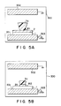
- Figs. 5A to 5F are cross-sectional views illustrating the steps of a process for fabricating a semiconductor device according to the fourth embodiment.
- a parallel plate type RIE apparatus 300 has a lower electrode 301, to which an AC source 303 is connected, and an upper electrode 302 serving as an ion generating source facing the lower electrode 301.
- a substrate 1 having a photoresist pattern 3a is placed on the lower electrode 301.
- the frequency of the RF generator 303 is about 200 KHz
- the thickness of the resist pattern 3a is about 1.5 ⁇ m.
- ions are emitted from the upper electrode 302 to etch a polysilicon layer 2 selectively, using the resist pattern 3a as mask.
- Fig. 5B shows the state in which the etching has been completed.
- the temperature of the upper electrode 302 is made to differ from that of the lower electrode 301, thus providing a temperature gradient therebetween.
- the inclination angle ⁇ 2 of the side wall of the polysilicon pattern 2a can be controlled.
- the inclination angle ⁇ 1 was 108° and the temperature of both the upper and lower electrodes 302 and 301 was set at 50°C
- the inclination angle ⁇ 2 was 113°.
- the inclination angle ⁇ 1 was 108° and the temperature of the upper electrode 302 was set at 60°C and that of the lower electrode 301 was set at 20°C, the inclination angle ⁇ 2 was 118°.
- the inclination angle ⁇ 1 was 112°C and the temperature of both the upper and lower electrodes 302 and 301 was set at 50°C
- the inclination angle ⁇ 2 was 127°C.
- the inclination angle ⁇ 1 was 112°C and the temperature of the upper electrode 302 was set at 60°C and that of the lower electrode 301 was set at 20°C, the inclination angle ⁇ 2 was 130°.
- the inclination angle ⁇ 2 of the side wall of the thin film pattern 2a can be controlled.
- the temperature gradient be provided such that the temperature of the lower electrode 301 be lower than that of the upper electrode 302.
- the thin film pattern was formed of an undoped or low-impurity-concentration polysilicon; however, any type of thin film capable of being subjected to isotropic etching may be employed (e.g. a high-impurity-concentration polysilicon, a silicon oxide film, a metallic film of aluminum, etc.).
- thin film formed over the thin film pattern is not limited to the high-impurity concentration polysilicon; for example, any type of thin film capable of being subjected to isotropic etching may be employed (e.g. an undoped polysilicon, a silicon oxide film, a metallic film of aluminum, etc.).
- the thin film can be etched by means of dry etching as much as possible, without lowering the reliability of the semiconductor device. Accordingly, semiconductor devices having fine element structure can be fabricated with a high yield, and this contributes to the development in miniaturization of element structure.
- a minimum rule of a resist pattern obtained by an image reverse method is about 0.8 ⁇ m. It is thought, however, that the minimum rule decreases to less than 0.8 ⁇ m, for example, a half micron or a quarter micron. Needless to say, the present invention is applicable, even if the minimum rule of a resist pattern having an inverted-trapezoidal cross section becomes a half micron or a quarter micron.
Landscapes
- Physics & Mathematics (AREA)
- General Physics & Mathematics (AREA)
- Drying Of Semiconductors (AREA)
- Exposure Of Semiconductors, Excluding Electron Or Ion Beam Exposure (AREA)
- Exposure And Positioning Against Photoresist Photosensitive Materials (AREA)
- Semiconductor Integrated Circuits (AREA)
Applications Claiming Priority (2)
| Application Number | Priority Date | Filing Date | Title |
|---|---|---|---|
| JP130042/90 | 1990-05-18 | ||
| JP2130042A JP2577488B2 (ja) | 1990-05-18 | 1990-05-18 | 半導体装置の製造方法 |
Publications (3)
| Publication Number | Publication Date |
|---|---|
| EP0459252A2 true EP0459252A2 (de) | 1991-12-04 |
| EP0459252A3 EP0459252A3 (en) | 1992-03-18 |
| EP0459252B1 EP0459252B1 (de) | 1996-07-10 |
Family
ID=15024690
Family Applications (1)
| Application Number | Title | Priority Date | Filing Date |
|---|---|---|---|
| EP91108046A Expired - Lifetime EP0459252B1 (de) | 1990-05-18 | 1991-05-17 | Herstellungsverfahren für ein Dünnschichtmuster mit trapezförmigem Querschnitt |
Country Status (5)
| Country | Link |
|---|---|
| US (1) | US5127989A (de) |
| EP (1) | EP0459252B1 (de) |
| JP (1) | JP2577488B2 (de) |
| KR (1) | KR940004409B1 (de) |
| DE (1) | DE69120729T2 (de) |
Cited By (1)
| Publication number | Priority date | Publication date | Assignee | Title |
|---|---|---|---|---|
| WO1995013567A1 (en) * | 1993-11-08 | 1995-05-18 | Alliedsignal Inc. | Process for making an array of tapered photopolymerized waveguides |
Families Citing this family (18)
| Publication number | Priority date | Publication date | Assignee | Title |
|---|---|---|---|---|
| US5234633A (en) * | 1987-12-28 | 1993-08-10 | Canon Kabushiki Kaisha | Cast molding die and process for producing information recording medium using the same |
| JP2759582B2 (ja) * | 1991-09-05 | 1998-05-28 | 三菱電機株式会社 | フォトマスクおよびその製造方法 |
| US5948232A (en) * | 1995-06-19 | 1999-09-07 | Lynntech, Inc. | Method of manufacturing passive elements using conductive polypyrrole formulations |
| US5722162A (en) * | 1995-10-12 | 1998-03-03 | Fujitsu Limited | Fabrication procedure for a stable post |
| US6117345A (en) * | 1997-04-02 | 2000-09-12 | United Microelectronics Corp. | High density plasma chemical vapor deposition process |
| US6232229B1 (en) | 1999-11-19 | 2001-05-15 | Micron Technology, Inc. | Microelectronic device fabricating method, integrated circuit, and intermediate construction |
| US20060199111A1 (en) * | 2005-03-01 | 2006-09-07 | Taiwan Semiconductor Manufacturing Company, Ltd. | Method for manufacturing semiconductor devices using a photo acid generator |
| CN100477327C (zh) * | 2005-10-09 | 2009-04-08 | 胜华科技股份有限公司 | 电极隔离壁 |
| KR101674208B1 (ko) * | 2009-12-29 | 2016-11-23 | 엘지디스플레이 주식회사 | 배선 형성 방법 및 이를 이용한 액정표시장치 제조방법 |
| CN106024982A (zh) * | 2016-07-11 | 2016-10-12 | 中国科学院上海技术物理研究所 | 一种红外焦平面芯片的铟柱制备方法 |
| US10731210B2 (en) | 2017-02-01 | 2020-08-04 | Seagate Technology Llc | Fabrication of nanochannel with integrated electrodes for DNA sequencing using tunneling current |
| US10640827B2 (en) | 2017-02-01 | 2020-05-05 | Seagate Technology Llc | Fabrication of wedge shaped electrode for enhanced DNA sequencing using tunneling current |
| US10641726B2 (en) | 2017-02-01 | 2020-05-05 | Seagate Technology Llc | Fabrication of a nanochannel for DNA sequencing using electrical plating to achieve tunneling electrode gap |
| US10889857B2 (en) | 2017-02-01 | 2021-01-12 | Seagate Technology Llc | Method to fabricate a nanochannel for DNA sequencing based on narrow trench patterning process |
| US10761058B2 (en) | 2017-02-01 | 2020-09-01 | Seagate Technology Llc | Nanostructures to control DNA strand orientation and position location for transverse DNA sequencing |
| US10752947B2 (en) | 2017-03-09 | 2020-08-25 | Seagate Technology Llc | Method to amplify transverse tunneling current discrimination of DNA nucleotides via nucleotide site specific attachment of dye-peptide |
| US20180259475A1 (en) | 2017-03-09 | 2018-09-13 | Seagate Technology Llc | Vertical nanopore coupled with a pair of transverse electrodes having a uniform ultrasmall nanogap for dna sequencing |
| CN112882343A (zh) * | 2021-01-15 | 2021-06-01 | 广州爱思威科技股份有限公司 | 光刻胶倒梯形结构的形成方法 |
Family Cites Families (7)
| Publication number | Priority date | Publication date | Assignee | Title |
|---|---|---|---|---|
| DE3175488D1 (en) * | 1981-02-07 | 1986-11-20 | Ibm Deutschland | Process for the formation and the filling of holes in a layer applied to a substrate |
| JPS60263964A (ja) * | 1984-06-13 | 1985-12-27 | Konishiroku Photo Ind Co Ltd | 画像記録装置 |
| JPS61227059A (ja) * | 1985-03-30 | 1986-10-09 | Ricoh Co Ltd | 偏向制御インクジエツト記録装置 |
| JPS62176873A (ja) * | 1986-01-31 | 1987-08-03 | Mita Ind Co Ltd | 粉体トナ−を用いた記録方法及び装置 |
| DE3615519A1 (de) * | 1986-05-07 | 1987-11-12 | Siemens Ag | Verfahren zum erzeugen von kontaktloechern mit abgeschraegten flanken in zwischenoxidschichten |
| US5007984A (en) * | 1987-09-28 | 1991-04-16 | Mitsubishi Denki Kabushiki Kaisha | Method for etching chromium film formed on substrate |
| US5007982A (en) * | 1988-07-11 | 1991-04-16 | North American Philips Corporation | Reactive ion etching of silicon with hydrogen bromide |
-
1990
- 1990-05-18 JP JP2130042A patent/JP2577488B2/ja not_active Expired - Fee Related
-
1991
- 1991-05-13 US US07/699,327 patent/US5127989A/en not_active Expired - Lifetime
- 1991-05-17 KR KR1019910008072A patent/KR940004409B1/ko not_active Expired - Fee Related
- 1991-05-17 EP EP91108046A patent/EP0459252B1/de not_active Expired - Lifetime
- 1991-05-17 DE DE69120729T patent/DE69120729T2/de not_active Expired - Fee Related
Cited By (2)
| Publication number | Priority date | Publication date | Assignee | Title |
|---|---|---|---|---|
| WO1995013567A1 (en) * | 1993-11-08 | 1995-05-18 | Alliedsignal Inc. | Process for making an array of tapered photopolymerized waveguides |
| US5462700A (en) * | 1993-11-08 | 1995-10-31 | Alliedsignal Inc. | Process for making an array of tapered photopolymerized waveguides |
Also Published As
| Publication number | Publication date |
|---|---|
| EP0459252B1 (de) | 1996-07-10 |
| EP0459252A3 (en) | 1992-03-18 |
| KR910020838A (ko) | 1991-12-20 |
| JPH0425126A (ja) | 1992-01-28 |
| DE69120729D1 (de) | 1996-08-14 |
| KR940004409B1 (ko) | 1994-05-25 |
| DE69120729T2 (de) | 1996-12-05 |
| JP2577488B2 (ja) | 1997-01-29 |
| US5127989A (en) | 1992-07-07 |
Similar Documents
| Publication | Publication Date | Title |
|---|---|---|
| EP0459252B1 (de) | Herstellungsverfahren für ein Dünnschichtmuster mit trapezförmigem Querschnitt | |
| US4523976A (en) | Method for forming semiconductor devices | |
| EP0069854B1 (de) | Verfahren zur Herstellung von Löchern in isolierenden Schichten | |
| US4295924A (en) | Method for providing self-aligned conductor in a V-groove device | |
| US4985374A (en) | Making a semiconductor device with ammonia treatment of photoresist | |
| JP3218814B2 (ja) | 半導体装置の製造方法 | |
| JP2004247399A (ja) | 半導体装置の製造方法 | |
| EP0895656B1 (de) | Eine bildumkehrtechnik zu ausbildung kleiner strukturen in integrierten schaltkreisen | |
| KR960012259B1 (ko) | 반도체 장치의 제조방법 | |
| JP3119021B2 (ja) | 半導体装置のコンタクトホール形成方法 | |
| JP2000173996A (ja) | 半導体装置およびその製造方法 | |
| US5514625A (en) | Method of forming a wiring layer | |
| JPH0669153A (ja) | 微細コンタクト孔の形成方法 | |
| KR100396689B1 (ko) | 반도체소자의게이트제조방법 | |
| US6583037B2 (en) | Method for fabricating gate of semiconductor device | |
| KR100275934B1 (ko) | 반도체장치의 미세도전라인 형성방법 | |
| JPH06163482A (ja) | 半導体装置のコンタクトホール形成方法 | |
| JPH05283358A (ja) | 半導体装置のコンタクトホール形成方法 | |
| KR950000090B1 (ko) | 반도체장치의 제조방법 | |
| KR0165417B1 (ko) | 반도체 장치의 미세 패턴 제조방법 | |
| KR100218727B1 (ko) | 반도체 소자의 콘택홀 형성방법 | |
| CA1260627A (en) | Lithographic image size reduction photomask | |
| JP3149601B2 (ja) | 半導体装置のコンタクトホール形成方法 | |
| US6596591B1 (en) | Methods to form reduced dimension bit-line isolation in the manufacture of non-volatile memory devices | |
| KR930012119B1 (ko) | 소자분리 산화막 제조방법 |
Legal Events
| Date | Code | Title | Description |
|---|---|---|---|
| PUAI | Public reference made under article 153(3) epc to a published international application that has entered the european phase |
Free format text: ORIGINAL CODE: 0009012 |
|
| 17P | Request for examination filed |
Effective date: 19910517 |
|
| AK | Designated contracting states |
Kind code of ref document: A2 Designated state(s): DE FR GB |
|
| PUAL | Search report despatched |
Free format text: ORIGINAL CODE: 0009013 |
|
| AK | Designated contracting states |
Kind code of ref document: A3 Designated state(s): DE FR GB |
|
| 17Q | First examination report despatched |
Effective date: 19930910 |
|
| GRAH | Despatch of communication of intention to grant a patent |
Free format text: ORIGINAL CODE: EPIDOS IGRA |
|
| GRAA | (expected) grant |
Free format text: ORIGINAL CODE: 0009210 |
|
| AK | Designated contracting states |
Kind code of ref document: B1 Designated state(s): DE FR GB |
|
| GRAH | Despatch of communication of intention to grant a patent |
Free format text: ORIGINAL CODE: EPIDOS IGRA |
|
| REF | Corresponds to: |
Ref document number: 69120729 Country of ref document: DE Date of ref document: 19960814 |
|
| ET | Fr: translation filed | ||
| PLBE | No opposition filed within time limit |
Free format text: ORIGINAL CODE: 0009261 |
|
| STAA | Information on the status of an ep patent application or granted ep patent |
Free format text: STATUS: NO OPPOSITION FILED WITHIN TIME LIMIT |
|
| 26N | No opposition filed | ||
| REG | Reference to a national code |
Ref country code: GB Ref legal event code: 746 Effective date: 19981012 |
|
| REG | Reference to a national code |
Ref country code: FR Ref legal event code: D6 |
|
| REG | Reference to a national code |
Ref country code: GB Ref legal event code: IF02 |
|
| PGFP | Annual fee paid to national office [announced via postgrant information from national office to epo] |
Ref country code: FR Payment date: 20020508 Year of fee payment: 12 |
|
| PGFP | Annual fee paid to national office [announced via postgrant information from national office to epo] |
Ref country code: GB Payment date: 20020515 Year of fee payment: 12 |
|
| PGFP | Annual fee paid to national office [announced via postgrant information from national office to epo] |
Ref country code: DE Payment date: 20020522 Year of fee payment: 12 |
|
| PG25 | Lapsed in a contracting state [announced via postgrant information from national office to epo] |
Ref country code: GB Free format text: LAPSE BECAUSE OF NON-PAYMENT OF DUE FEES Effective date: 20030517 |
|
| PG25 | Lapsed in a contracting state [announced via postgrant information from national office to epo] |
Ref country code: DE Free format text: LAPSE BECAUSE OF NON-PAYMENT OF DUE FEES Effective date: 20031202 |
|
| GBPC | Gb: european patent ceased through non-payment of renewal fee |
Effective date: 20030517 |
|
| PG25 | Lapsed in a contracting state [announced via postgrant information from national office to epo] |
Ref country code: FR Free format text: LAPSE BECAUSE OF NON-PAYMENT OF DUE FEES Effective date: 20040130 |
|
| REG | Reference to a national code |
Ref country code: FR Ref legal event code: ST |