EP0454590B1 - Guide d'onde optique à partir de polyimide - Google Patents
Guide d'onde optique à partir de polyimide Download PDFInfo
- Publication number
- EP0454590B1 EP0454590B1 EP91401120A EP91401120A EP0454590B1 EP 0454590 B1 EP0454590 B1 EP 0454590B1 EP 91401120 A EP91401120 A EP 91401120A EP 91401120 A EP91401120 A EP 91401120A EP 0454590 B1 EP0454590 B1 EP 0454590B1
- Authority
- EP
- European Patent Office
- Prior art keywords
- layer
- polyimide
- solution
- optical waveguide
- bis
- Prior art date
- Legal status (The legal status is an assumption and is not a legal conclusion. Google has not performed a legal analysis and makes no representation as to the accuracy of the status listed.)
- Expired - Lifetime
Links
- 239000004642 Polyimide Substances 0.000 title claims description 189
- 229920001721 polyimide Polymers 0.000 title claims description 189
- 230000003287 optical effect Effects 0.000 title claims description 120
- 238000000034 method Methods 0.000 claims description 57
- 229920001519 homopolymer Polymers 0.000 claims description 55
- 229920005575 poly(amic acid) Polymers 0.000 claims description 51
- 238000010438 heat treatment Methods 0.000 claims description 43
- 239000002243 precursor Substances 0.000 claims description 42
- 239000000758 substrate Substances 0.000 claims description 25
- 150000004985 diamines Chemical class 0.000 claims description 21
- 239000000203 mixture Substances 0.000 claims description 14
- 230000005540 biological transmission Effects 0.000 claims description 8
- -1 tetracarboxylic acid dianhydride Chemical class 0.000 claims description 8
- 125000000962 organic group Chemical group 0.000 claims description 4
- 239000010410 layer Substances 0.000 description 135
- 238000005253 cladding Methods 0.000 description 60
- 239000012792 core layer Substances 0.000 description 46
- GTDPSWPPOUPBNX-UHFFFAOYSA-N ac1mqpva Chemical compound CC12C(=O)OC(=O)C1(C)C1(C)C2(C)C(=O)OC1=O GTDPSWPPOUPBNX-UHFFFAOYSA-N 0.000 description 34
- FXHOOIRPVKKKFG-UHFFFAOYSA-N N,N-Dimethylacetamide Chemical compound CN(C)C(C)=O FXHOOIRPVKKKFG-UHFFFAOYSA-N 0.000 description 25
- 238000004519 manufacturing process Methods 0.000 description 24
- 235000012431 wafers Nutrition 0.000 description 22
- VYPSYNLAJGMNEJ-UHFFFAOYSA-N Silicium dioxide Chemical compound O=[Si]=O VYPSYNLAJGMNEJ-UHFFFAOYSA-N 0.000 description 15
- XAGFODPZIPBFFR-UHFFFAOYSA-N aluminium Chemical compound [Al] XAGFODPZIPBFFR-UHFFFAOYSA-N 0.000 description 14
- 229910052782 aluminium Inorganic materials 0.000 description 14
- 238000005259 measurement Methods 0.000 description 13
- XUIMIQQOPSSXEZ-UHFFFAOYSA-N Silicon Chemical compound [Si] XUIMIQQOPSSXEZ-UHFFFAOYSA-N 0.000 description 9
- 229910052710 silicon Inorganic materials 0.000 description 9
- 239000010703 silicon Substances 0.000 description 9
- ZSIAUFGUXNUGDI-UHFFFAOYSA-N hexan-1-ol Chemical compound CCCCCCO ZSIAUFGUXNUGDI-UHFFFAOYSA-N 0.000 description 8
- 229910052814 silicon oxide Inorganic materials 0.000 description 8
- NVKGJHAQGWCWDI-UHFFFAOYSA-N 4-[4-amino-2-(trifluoromethyl)phenyl]-3-(trifluoromethyl)aniline Chemical group FC(F)(F)C1=CC(N)=CC=C1C1=CC=C(N)C=C1C(F)(F)F NVKGJHAQGWCWDI-UHFFFAOYSA-N 0.000 description 7
- 239000000463 material Substances 0.000 description 7
- 239000002904 solvent Substances 0.000 description 7
- RTZKZFJDLAIYFH-UHFFFAOYSA-N Diethyl ether Chemical compound CCOCC RTZKZFJDLAIYFH-UHFFFAOYSA-N 0.000 description 6
- KZTYYGOKRVBIMI-UHFFFAOYSA-N diphenyl sulfone Chemical compound C=1C=CC=CC=1S(=O)(=O)C1=CC=CC=C1 KZTYYGOKRVBIMI-UHFFFAOYSA-N 0.000 description 6
- 239000003960 organic solvent Substances 0.000 description 6
- 238000012545 processing Methods 0.000 description 6
- 125000002023 trifluoromethyl group Chemical group FC(F)(F)* 0.000 description 6
- 239000004033 plastic Substances 0.000 description 5
- 229920003023 plastic Polymers 0.000 description 5
- 239000002344 surface layer Substances 0.000 description 5
- 238000001039 wet etching Methods 0.000 description 5
- 238000000149 argon plasma sintering Methods 0.000 description 4
- 239000003795 chemical substances by application Substances 0.000 description 4
- 238000004891 communication Methods 0.000 description 4
- 238000011161 development Methods 0.000 description 4
- UHOVQNZJYSORNB-UHFFFAOYSA-N monobenzene Natural products C1=CC=CC=C1 UHOVQNZJYSORNB-UHFFFAOYSA-N 0.000 description 4
- 238000001020 plasma etching Methods 0.000 description 4
- 125000006158 tetracarboxylic acid group Chemical group 0.000 description 4
- 150000000000 tetracarboxylic acids Chemical class 0.000 description 4
- VLDPXPPHXDGHEW-UHFFFAOYSA-N 1-chloro-2-dichlorophosphoryloxybenzene Chemical compound ClC1=CC=CC=C1OP(Cl)(Cl)=O VLDPXPPHXDGHEW-UHFFFAOYSA-N 0.000 description 3
- ZMXDDKWLCZADIW-UHFFFAOYSA-N N,N-Dimethylformamide Chemical compound CN(C)C=O ZMXDDKWLCZADIW-UHFFFAOYSA-N 0.000 description 3
- AZDRQVAHHNSJOQ-UHFFFAOYSA-N alumane Chemical group [AlH3] AZDRQVAHHNSJOQ-UHFFFAOYSA-N 0.000 description 3
- 230000015572 biosynthetic process Effects 0.000 description 3
- 238000000354 decomposition reaction Methods 0.000 description 3
- 125000006159 dianhydride group Chemical group 0.000 description 3
- 238000001035 drying Methods 0.000 description 3
- 238000000313 electron-beam-induced deposition Methods 0.000 description 3
- 238000005516 engineering process Methods 0.000 description 3
- 239000003822 epoxy resin Substances 0.000 description 3
- 238000005530 etching Methods 0.000 description 3
- LNEPOXFFQSENCJ-UHFFFAOYSA-N haloperidol Chemical compound C1CC(O)(C=2C=CC(Cl)=CC=2)CCN1CCCC(=O)C1=CC=C(F)C=C1 LNEPOXFFQSENCJ-UHFFFAOYSA-N 0.000 description 3
- QSHDDOUJBYECFT-UHFFFAOYSA-N mercury Chemical compound [Hg] QSHDDOUJBYECFT-UHFFFAOYSA-N 0.000 description 3
- 229920000647 polyepoxide Polymers 0.000 description 3
- 230000005855 radiation Effects 0.000 description 3
- 238000005406 washing Methods 0.000 description 3
- APXJLYIVOFARRM-UHFFFAOYSA-N 4-[2-(3,4-dicarboxyphenyl)-1,1,1,3,3,3-hexafluoropropan-2-yl]phthalic acid Chemical compound C1=C(C(O)=O)C(C(=O)O)=CC=C1C(C(F)(F)F)(C(F)(F)F)C1=CC=C(C(O)=O)C(C(O)=O)=C1 APXJLYIVOFARRM-UHFFFAOYSA-N 0.000 description 2
- VQVIHDPBMFABCQ-UHFFFAOYSA-N 5-(1,3-dioxo-2-benzofuran-5-carbonyl)-2-benzofuran-1,3-dione Chemical compound C1=C2C(=O)OC(=O)C2=CC(C(C=2C=C3C(=O)OC(=O)C3=CC=2)=O)=C1 VQVIHDPBMFABCQ-UHFFFAOYSA-N 0.000 description 2
- YCKRFDGAMUMZLT-UHFFFAOYSA-N Fluorine atom Chemical compound [F] YCKRFDGAMUMZLT-UHFFFAOYSA-N 0.000 description 2
- SECXISVLQFMRJM-UHFFFAOYSA-N N-Methylpyrrolidone Chemical compound CN1CCCC1=O SECXISVLQFMRJM-UHFFFAOYSA-N 0.000 description 2
- 239000002253 acid Substances 0.000 description 2
- 229940076134 benzene Drugs 0.000 description 2
- 235000010290 biphenyl Nutrition 0.000 description 2
- 239000004305 biphenyl Substances 0.000 description 2
- 229920001577 copolymer Polymers 0.000 description 2
- 230000000694 effects Effects 0.000 description 2
- 150000002148 esters Chemical class 0.000 description 2
- 229910052731 fluorine Inorganic materials 0.000 description 2
- 239000011737 fluorine Substances 0.000 description 2
- 239000000178 monomer Substances 0.000 description 2
- 229910052757 nitrogen Inorganic materials 0.000 description 2
- 125000001997 phenyl group Chemical group [H]C1=C([H])C([H])=C(*)C([H])=C1[H] 0.000 description 2
- ZUOUZKKEUPVFJK-UHFFFAOYSA-N phenylbenzene Natural products C1=CC=CC=C1C1=CC=CC=C1 ZUOUZKKEUPVFJK-UHFFFAOYSA-N 0.000 description 2
- 229920003229 poly(methyl methacrylate) Polymers 0.000 description 2
- 229920000642 polymer Polymers 0.000 description 2
- 239000004926 polymethyl methacrylate Substances 0.000 description 2
- CYIDZMCFTVVTJO-UHFFFAOYSA-N pyromellitic acid Chemical compound OC(=O)C1=CC(C(O)=O)=C(C(O)=O)C=C1C(O)=O CYIDZMCFTVVTJO-UHFFFAOYSA-N 0.000 description 2
- 238000005476 soldering Methods 0.000 description 2
- 125000001424 substituent group Chemical group 0.000 description 2
- XLYOFNOQVPJJNP-UHFFFAOYSA-N water Substances O XLYOFNOQVPJJNP-UHFFFAOYSA-N 0.000 description 2
- OFXSBTTVJAFNSJ-UHFFFAOYSA-N 1,1,2,2,3,3,4,4,5,5,6,6,7,7-tetradecafluoro-n,n'-diphenylheptane-1,7-diamine Chemical compound C=1C=CC=CC=1NC(F)(F)C(F)(F)C(F)(F)C(F)(F)C(F)(F)C(F)(F)C(F)(F)NC1=CC=CC=C1 OFXSBTTVJAFNSJ-UHFFFAOYSA-N 0.000 description 1
- VITYLMJSEZETGU-UHFFFAOYSA-N 1,1,2,2,3,3,4,4,5,5-decafluoro-n,n'-diphenylpentane-1,5-diamine Chemical compound C=1C=CC=CC=1NC(F)(F)C(F)(F)C(F)(F)C(F)(F)C(F)(F)NC1=CC=CC=C1 VITYLMJSEZETGU-UHFFFAOYSA-N 0.000 description 1
- JLTHXLWCVUJTFW-UHFFFAOYSA-N 1,1,2,2,3,3,4,4-octafluoro-n,n'-diphenylbutane-1,4-diamine Chemical compound C=1C=CC=CC=1NC(F)(F)C(F)(F)C(F)(F)C(F)(F)NC1=CC=CC=C1 JLTHXLWCVUJTFW-UHFFFAOYSA-N 0.000 description 1
- UMMYYBOQOTWQTD-UHFFFAOYSA-N 1,1,2,2,3,3-hexafluoro-n,n'-diphenylpropane-1,3-diamine Chemical compound C=1C=CC=CC=1NC(F)(F)C(F)(F)C(F)(F)NC1=CC=CC=C1 UMMYYBOQOTWQTD-UHFFFAOYSA-N 0.000 description 1
- LRMDXTVKVHKWEK-UHFFFAOYSA-N 1,2-diaminoanthracene-9,10-dione Chemical compound C1=CC=C2C(=O)C3=C(N)C(N)=CC=C3C(=O)C2=C1 LRMDXTVKVHKWEK-UHFFFAOYSA-N 0.000 description 1
- WZCQRUWWHSTZEM-UHFFFAOYSA-N 1,3-phenylenediamine Chemical compound NC1=CC=CC(N)=C1 WZCQRUWWHSTZEM-UHFFFAOYSA-N 0.000 description 1
- CBCKQZAAMUWICA-UHFFFAOYSA-N 1,4-phenylenediamine Chemical compound NC1=CC=C(N)C=C1 CBCKQZAAMUWICA-UHFFFAOYSA-N 0.000 description 1
- WCZNKVPCIFMXEQ-UHFFFAOYSA-N 2,3,5,6-tetramethylbenzene-1,4-diamine Chemical compound CC1=C(C)C(N)=C(C)C(C)=C1N WCZNKVPCIFMXEQ-UHFFFAOYSA-N 0.000 description 1
- VOZKAJLKRJDJLL-UHFFFAOYSA-N 2,4-diaminotoluene Chemical compound CC1=CC=C(N)C=C1N VOZKAJLKRJDJLL-UHFFFAOYSA-N 0.000 description 1
- 229940075142 2,5-diaminotoluene Drugs 0.000 description 1
- LWKVCPHDFUTUGP-UHFFFAOYSA-N 2-(1,1,2,2,3,3,4,4,4-nonafluorobutyl)benzene-1,4-diamine Chemical compound NC1=CC=C(N)C(C(F)(F)C(F)(F)C(F)(F)C(F)(F)F)=C1 LWKVCPHDFUTUGP-UHFFFAOYSA-N 0.000 description 1
- POEYBOBCTDQWLL-UHFFFAOYSA-N 2-(1,1,2,2,3,3,4,4,5,5,6,6,6-tridecafluorohexyl)benzene-1,4-diamine Chemical compound NC1=CC=C(N)C(C(F)(F)C(F)(F)C(F)(F)C(F)(F)C(F)(F)C(F)(F)F)=C1 POEYBOBCTDQWLL-UHFFFAOYSA-N 0.000 description 1
- ZQQOGBKIFPCFMJ-UHFFFAOYSA-N 2-(trifluoromethyl)benzene-1,4-diamine Chemical compound NC1=CC=C(N)C(C(F)(F)F)=C1 ZQQOGBKIFPCFMJ-UHFFFAOYSA-N 0.000 description 1
- IOHPPIBXAKZWGA-UHFFFAOYSA-N 2-[2-(2-aminophenoxy)-3,4,5,6-tetrakis(trifluoromethyl)phenoxy]aniline Chemical compound NC1=CC=CC=C1OC(C(=C(C(=C1C(F)(F)F)C(F)(F)F)C(F)(F)F)C(F)(F)F)=C1OC1=CC=CC=C1N IOHPPIBXAKZWGA-UHFFFAOYSA-N 0.000 description 1
- KDGNBLYSSKCVAN-UHFFFAOYSA-N 2-[2-(2-aminophenoxy)-3,4-bis(trifluoromethyl)phenoxy]aniline Chemical compound NC1=CC=CC=C1OC1=CC=C(C(F)(F)F)C(C(F)(F)F)=C1OC1=CC=CC=C1N KDGNBLYSSKCVAN-UHFFFAOYSA-N 0.000 description 1
- YUZSJKBFHATJHV-UHFFFAOYSA-N 2-[4-[2-[4-(2-aminophenoxy)phenyl]-1,1,1,3,3,3-hexafluoropropan-2-yl]phenoxy]aniline Chemical compound NC1=CC=CC=C1OC1=CC=C(C(C=2C=CC(OC=3C(=CC=CC=3)N)=CC=2)(C(F)(F)F)C(F)(F)F)C=C1 YUZSJKBFHATJHV-UHFFFAOYSA-N 0.000 description 1
- OBCSAIDCZQSFQH-UHFFFAOYSA-N 2-methyl-1,4-phenylenediamine Chemical compound CC1=CC(N)=CC=C1N OBCSAIDCZQSFQH-UHFFFAOYSA-N 0.000 description 1
- UAIUNKRWKOVEES-UHFFFAOYSA-N 3,3',5,5'-tetramethylbenzidine Chemical compound CC1=C(N)C(C)=CC(C=2C=C(C)C(N)=C(C)C=2)=C1 UAIUNKRWKOVEES-UHFFFAOYSA-N 0.000 description 1
- JRBJSXQPQWSCCF-UHFFFAOYSA-N 3,3'-Dimethoxybenzidine Chemical compound C1=C(N)C(OC)=CC(C=2C=C(OC)C(N)=CC=2)=C1 JRBJSXQPQWSCCF-UHFFFAOYSA-N 0.000 description 1
- NUIURNJTPRWVAP-UHFFFAOYSA-N 3,3'-Dimethylbenzidine Chemical compound C1=C(N)C(C)=CC(C=2C=C(C)C(N)=CC=2)=C1 NUIURNJTPRWVAP-UHFFFAOYSA-N 0.000 description 1
- PWTKZYBDXDXRMR-UHFFFAOYSA-N 3,4,5,6-tetrakis(trifluoromethyl)benzene-1,2-diamine Chemical compound NC1=C(N)C(C(F)(F)F)=C(C(F)(F)F)C(C(F)(F)F)=C1C(F)(F)F PWTKZYBDXDXRMR-UHFFFAOYSA-N 0.000 description 1
- BDSPLIQKGRTNCG-UHFFFAOYSA-N 3,4-dimethylcyclohexa-1,5-diene-1,3-diamine Chemical group CC1C=CC(N)=CC1(C)N BDSPLIQKGRTNCG-UHFFFAOYSA-N 0.000 description 1
- WRTHJTIPFDXAGH-UHFFFAOYSA-N 3-(1,1,2,2,2-pentafluoroethyl)benzene-1,2-diamine Chemical compound NC1=CC=CC(C(F)(F)C(F)(F)F)=C1N WRTHJTIPFDXAGH-UHFFFAOYSA-N 0.000 description 1
- OLQWMCSSZKNOLQ-UHFFFAOYSA-N 3-(2,5-dioxooxolan-3-yl)oxolane-2,5-dione Chemical compound O=C1OC(=O)CC1C1C(=O)OC(=O)C1 OLQWMCSSZKNOLQ-UHFFFAOYSA-N 0.000 description 1
- JAUWPCNIJHYPGO-UHFFFAOYSA-N 3-[2-(2,3-dicarboxyphenoxy)-3,4,5,6-tetrakis(trifluoromethyl)phenoxy]phthalic acid Chemical compound OC(=O)C1=CC=CC(OC=2C(=C(C(=C(C=2OC=2C(=C(C(O)=O)C=CC=2)C(O)=O)C(F)(F)F)C(F)(F)F)C(F)(F)F)C(F)(F)F)=C1C(O)=O JAUWPCNIJHYPGO-UHFFFAOYSA-N 0.000 description 1
- GIDZGEJVGCDPLV-UHFFFAOYSA-N 3-[2-(2,3-dicarboxyphenoxy)-3,4-bis(trifluoromethyl)phenoxy]phthalic acid Chemical compound OC(=O)C1=CC=CC(OC=2C(=C(C(=CC=2)C(F)(F)F)C(F)(F)F)OC=2C(=C(C(O)=O)C=CC=2)C(O)=O)=C1C(O)=O GIDZGEJVGCDPLV-UHFFFAOYSA-N 0.000 description 1
- QBQWCUVAROAAQA-UHFFFAOYSA-N 3-[2-(2,3-dicarboxyphenoxy)-3-(trifluoromethyl)phenoxy]phthalic acid Chemical compound OC(=O)C1=CC=CC(OC=2C(=C(C=CC=2)C(F)(F)F)OC=2C(=C(C(O)=O)C=CC=2)C(O)=O)=C1C(O)=O QBQWCUVAROAAQA-UHFFFAOYSA-N 0.000 description 1
- MFTFTIALAXXIMU-UHFFFAOYSA-N 3-[4-[2-[4-(3-aminophenoxy)phenyl]-1,1,1,3,3,3-hexafluoropropan-2-yl]phenoxy]aniline Chemical compound NC1=CC=CC(OC=2C=CC(=CC=2)C(C=2C=CC(OC=3C=C(N)C=CC=3)=CC=2)(C(F)(F)F)C(F)(F)F)=C1 MFTFTIALAXXIMU-UHFFFAOYSA-N 0.000 description 1
- WECDUOXQLAIPQW-UHFFFAOYSA-N 4,4'-Methylene bis(2-methylaniline) Chemical compound C1=C(N)C(C)=CC(CC=2C=C(C)C(N)=CC=2)=C1 WECDUOXQLAIPQW-UHFFFAOYSA-N 0.000 description 1
- YBRVSVVVWCFQMG-UHFFFAOYSA-N 4,4'-diaminodiphenylmethane Chemical compound C1=CC(N)=CC=C1CC1=CC=C(N)C=C1 YBRVSVVVWCFQMG-UHFFFAOYSA-N 0.000 description 1
- FYYYKXFEKMGYLZ-UHFFFAOYSA-N 4-(1,3-dioxo-2-benzofuran-5-yl)-2-benzofuran-1,3-dione Chemical compound C=1C=C2C(=O)OC(=O)C2=CC=1C1=CC=CC2=C1C(=O)OC2=O FYYYKXFEKMGYLZ-UHFFFAOYSA-N 0.000 description 1
- QHZDSYDKTZORNZ-UHFFFAOYSA-N 4-(2,3,5,6-tetrafluorophenoxy)benzene-1,3-diamine Chemical compound NC1=CC(N)=CC=C1OC1=C(F)C(F)=CC(F)=C1F QHZDSYDKTZORNZ-UHFFFAOYSA-N 0.000 description 1
- FWOLORXQTIGHFX-UHFFFAOYSA-N 4-(4-amino-2,3,5,6-tetrafluorophenyl)-2,3,5,6-tetrafluoroaniline Chemical compound FC1=C(F)C(N)=C(F)C(F)=C1C1=C(F)C(F)=C(N)C(F)=C1F FWOLORXQTIGHFX-UHFFFAOYSA-N 0.000 description 1
- YJOAIOIVLVUPST-UHFFFAOYSA-N 4-(4-amino-2-methoxyphenyl)-3-methoxyaniline Chemical compound COC1=CC(N)=CC=C1C1=CC=C(N)C=C1OC YJOAIOIVLVUPST-UHFFFAOYSA-N 0.000 description 1
- QYIMZXITLDTULQ-UHFFFAOYSA-N 4-(4-amino-2-methylphenyl)-3-methylaniline Chemical compound CC1=CC(N)=CC=C1C1=CC=C(N)C=C1C QYIMZXITLDTULQ-UHFFFAOYSA-N 0.000 description 1
- OSOMJBMUSWZQME-UHFFFAOYSA-N 4-(4-fluorophenoxy)benzene-1,3-diamine Chemical compound NC1=CC(N)=CC=C1OC1=CC=C(F)C=C1 OSOMJBMUSWZQME-UHFFFAOYSA-N 0.000 description 1
- HLBLWEWZXPIGSM-UHFFFAOYSA-N 4-Aminophenyl ether Chemical compound C1=CC(N)=CC=C1OC1=CC=C(N)C=C1 HLBLWEWZXPIGSM-UHFFFAOYSA-N 0.000 description 1
- GEYAGBVEAJGCFB-UHFFFAOYSA-N 4-[2-(3,4-dicarboxyphenyl)propan-2-yl]phthalic acid Chemical compound C=1C=C(C(O)=O)C(C(O)=O)=CC=1C(C)(C)C1=CC=C(C(O)=O)C(C(O)=O)=C1 GEYAGBVEAJGCFB-UHFFFAOYSA-N 0.000 description 1
- BEKFRNOZJSYWKZ-UHFFFAOYSA-N 4-[2-(4-aminophenyl)-1,1,1,3,3,3-hexafluoropropan-2-yl]aniline Chemical compound C1=CC(N)=CC=C1C(C(F)(F)F)(C(F)(F)F)C1=CC=C(N)C=C1 BEKFRNOZJSYWKZ-UHFFFAOYSA-N 0.000 description 1
- ZYEDGEXYGKWJPB-UHFFFAOYSA-N 4-[2-(4-aminophenyl)propan-2-yl]aniline Chemical compound C=1C=C(N)C=CC=1C(C)(C)C1=CC=C(N)C=C1 ZYEDGEXYGKWJPB-UHFFFAOYSA-N 0.000 description 1
- QBSMHWVGUPQNJJ-UHFFFAOYSA-N 4-[4-(4-aminophenyl)phenyl]aniline Chemical compound C1=CC(N)=CC=C1C1=CC=C(C=2C=CC(N)=CC=2)C=C1 QBSMHWVGUPQNJJ-UHFFFAOYSA-N 0.000 description 1
- IOUVQFAYPGDXFG-UHFFFAOYSA-N 4-[4-[2-[4-(3,4-dicarboxyphenoxy)phenyl]-1,1,1,3,3,3-hexafluoropropan-2-yl]phenoxy]phthalic acid Chemical compound C1=C(C(O)=O)C(C(=O)O)=CC=C1OC1=CC=C(C(C=2C=CC(OC=3C=C(C(C(O)=O)=CC=3)C(O)=O)=CC=2)(C(F)(F)F)C(F)(F)F)C=C1 IOUVQFAYPGDXFG-UHFFFAOYSA-N 0.000 description 1
- HBLYIUPUXAWDMA-UHFFFAOYSA-N 4-[4-[2-[4-(4-aminophenoxy)-3,5-bis(trifluoromethyl)phenyl]-1,1,1,3,3,3-hexafluoropropan-2-yl]-2,6-bis(trifluoromethyl)phenoxy]aniline Chemical compound C1=CC(N)=CC=C1OC1=C(C(F)(F)F)C=C(C(C=2C=C(C(OC=3C=CC(N)=CC=3)=C(C=2)C(F)(F)F)C(F)(F)F)(C(F)(F)F)C(F)(F)F)C=C1C(F)(F)F HBLYIUPUXAWDMA-UHFFFAOYSA-N 0.000 description 1
- VCFYKCXKADGLPS-UHFFFAOYSA-N 4-[4-[2-[4-(4-aminophenoxy)-3,5-dimethylphenyl]-1,1,1,3,3,3-hexafluoropropan-2-yl]-2,6-dimethylphenoxy]aniline Chemical compound CC1=CC(C(C=2C=C(C)C(OC=3C=CC(N)=CC=3)=C(C)C=2)(C(F)(F)F)C(F)(F)F)=CC(C)=C1OC1=CC=C(N)C=C1 VCFYKCXKADGLPS-UHFFFAOYSA-N 0.000 description 1
- HHLMWQDRYZAENA-UHFFFAOYSA-N 4-[4-[2-[4-(4-aminophenoxy)phenyl]-1,1,1,3,3,3-hexafluoropropan-2-yl]phenoxy]aniline Chemical compound C1=CC(N)=CC=C1OC1=CC=C(C(C=2C=CC(OC=3C=CC(N)=CC=3)=CC=2)(C(F)(F)F)C(F)(F)F)C=C1 HHLMWQDRYZAENA-UHFFFAOYSA-N 0.000 description 1
- KMKWGXGSGPYISJ-UHFFFAOYSA-N 4-[4-[2-[4-(4-aminophenoxy)phenyl]propan-2-yl]phenoxy]aniline Chemical compound C=1C=C(OC=2C=CC(N)=CC=2)C=CC=1C(C)(C)C(C=C1)=CC=C1OC1=CC=C(N)C=C1 KMKWGXGSGPYISJ-UHFFFAOYSA-N 0.000 description 1
- PDYQWKUIJVOAON-UHFFFAOYSA-N 4-[4-[2-[4-[4-amino-3-(trifluoromethyl)phenoxy]phenyl]-1,1,1,3,3,3-hexafluoropropan-2-yl]phenoxy]-2-(trifluoromethyl)aniline Chemical compound C1=C(C(F)(F)F)C(N)=CC=C1OC1=CC=C(C(C=2C=CC(OC=3C=C(C(N)=CC=3)C(F)(F)F)=CC=2)(C(F)(F)F)C(F)(F)F)C=C1 PDYQWKUIJVOAON-UHFFFAOYSA-N 0.000 description 1
- HYDATEKARGDBKU-UHFFFAOYSA-N 4-[4-[4-(4-aminophenoxy)phenyl]phenoxy]aniline Chemical group C1=CC(N)=CC=C1OC1=CC=C(C=2C=CC(OC=3C=CC(N)=CC=3)=CC=2)C=C1 HYDATEKARGDBKU-UHFFFAOYSA-N 0.000 description 1
- JZIAOTUERDUSJC-UHFFFAOYSA-N 4-[4-[4-(4-aminophenyl)phenyl]phenyl]aniline Chemical group C1=CC(N)=CC=C1C1=CC=C(C=2C=CC(=CC=2)C=2C=CC(N)=CC=2)C=C1 JZIAOTUERDUSJC-UHFFFAOYSA-N 0.000 description 1
- IWFSADBGACLBMH-UHFFFAOYSA-N 4-[4-[4-[4-amino-2-(trifluoromethyl)phenoxy]phenyl]phenoxy]-3-(trifluoromethyl)aniline Chemical group FC(F)(F)C1=CC(N)=CC=C1OC1=CC=C(C=2C=CC(OC=3C(=CC(N)=CC=3)C(F)(F)F)=CC=2)C=C1 IWFSADBGACLBMH-UHFFFAOYSA-N 0.000 description 1
- DPCDFSDBIWVMJC-UHFFFAOYSA-N 4-[4-[4-[4-amino-3-(trifluoromethyl)phenoxy]phenyl]phenoxy]-2-(trifluoromethyl)aniline Chemical group C1=C(C(F)(F)F)C(N)=CC=C1OC1=CC=C(C=2C=CC(OC=3C=C(C(N)=CC=3)C(F)(F)F)=CC=2)C=C1 DPCDFSDBIWVMJC-UHFFFAOYSA-N 0.000 description 1
- LACZRKUWKHQVKS-UHFFFAOYSA-N 4-[4-[4-amino-2-(trifluoromethyl)phenoxy]phenoxy]-3-(trifluoromethyl)aniline Chemical compound FC(F)(F)C1=CC(N)=CC=C1OC(C=C1)=CC=C1OC1=CC=C(N)C=C1C(F)(F)F LACZRKUWKHQVKS-UHFFFAOYSA-N 0.000 description 1
- NKYXYJFTTIPZDE-UHFFFAOYSA-N 4-[4-amino-2-(trifluoromethyl)phenoxy]-3-(trifluoromethyl)aniline Chemical compound FC(F)(F)C1=CC(N)=CC=C1OC1=CC=C(N)C=C1C(F)(F)F NKYXYJFTTIPZDE-UHFFFAOYSA-N 0.000 description 1
- PJWQLRKRVISYPL-UHFFFAOYSA-N 4-[4-amino-3-(trifluoromethyl)phenyl]-2-(trifluoromethyl)aniline Chemical group C1=C(C(F)(F)F)C(N)=CC=C1C1=CC=C(N)C(C(F)(F)F)=C1 PJWQLRKRVISYPL-UHFFFAOYSA-N 0.000 description 1
- DNQIDXZMLCPYPU-UHFFFAOYSA-N 5-[3,4-dicarboxy-5-(trifluoromethyl)benzoyl]-3-(trifluoromethyl)phthalic acid Chemical compound FC(F)(F)C1=C(C(O)=O)C(C(=O)O)=CC(C(=O)C=2C=C(C(C(O)=O)=C(C(O)=O)C=2)C(F)(F)F)=C1 DNQIDXZMLCPYPU-UHFFFAOYSA-N 0.000 description 1
- MQAHXEQUBNDFGI-UHFFFAOYSA-N 5-[4-[2-[4-[(1,3-dioxo-2-benzofuran-5-yl)oxy]phenyl]propan-2-yl]phenoxy]-2-benzofuran-1,3-dione Chemical compound C1=C2C(=O)OC(=O)C2=CC(OC2=CC=C(C=C2)C(C)(C=2C=CC(OC=3C=C4C(=O)OC(=O)C4=CC=3)=CC=2)C)=C1 MQAHXEQUBNDFGI-UHFFFAOYSA-N 0.000 description 1
- JTYBYCLEGGNJKI-UHFFFAOYSA-N Cc1c(C(F)(F)F)c(C)c(C)c(C(F)(F)F)c1C Chemical compound Cc1c(C(F)(F)F)c(C)c(C)c(C(F)(F)F)c1C JTYBYCLEGGNJKI-UHFFFAOYSA-N 0.000 description 1
- GLFKFHJEFMLTOB-UHFFFAOYSA-N Cc1c(C)cc(C(C(F)(F)F)(C(F)(F)F)c2cc(C)c(C)cc2)cc1 Chemical compound Cc1c(C)cc(C(C(F)(F)F)(C(F)(F)F)c2cc(C)c(C)cc2)cc1 GLFKFHJEFMLTOB-UHFFFAOYSA-N 0.000 description 1
- JNFNQQBFUUZQRM-UHFFFAOYSA-N Cc1cc(I)c(C)c(C(F)(F)F)c1C Chemical compound Cc1cc(I)c(C)c(C(F)(F)F)c1C JNFNQQBFUUZQRM-UHFFFAOYSA-N 0.000 description 1
- MQJKPEGWNLWLTK-UHFFFAOYSA-N Dapsone Chemical compound C1=CC(N)=CC=C1S(=O)(=O)C1=CC=C(N)C=C1 MQJKPEGWNLWLTK-UHFFFAOYSA-N 0.000 description 1
- LFQSCWFLJHTTHZ-UHFFFAOYSA-N Ethanol Chemical compound CCO LFQSCWFLJHTTHZ-UHFFFAOYSA-N 0.000 description 1
- ZEGLXFHIJNPVNE-UHFFFAOYSA-N FC(F)(F)NC1=C(C=CC=C1)NC(F)(F)F Chemical compound FC(F)(F)NC1=C(C=CC=C1)NC(F)(F)F ZEGLXFHIJNPVNE-UHFFFAOYSA-N 0.000 description 1
- HQHZDNOKSOTOHQ-UHFFFAOYSA-N FC(F)(F)NC1=C(OC2=C(C=CC=C2)C(C(F)(F)F)(C(F)(F)F)C2=C(C=CC=C2)OC2=C(C=CC=C2)NC(F)(F)F)C=CC=C1 Chemical compound FC(F)(F)NC1=C(OC2=C(C=CC=C2)C(C(F)(F)F)(C(F)(F)F)C2=C(C=CC=C2)OC2=C(C=CC=C2)NC(F)(F)F)C=CC=C1 HQHZDNOKSOTOHQ-UHFFFAOYSA-N 0.000 description 1
- NTIZESTWPVYFNL-UHFFFAOYSA-N Methyl isobutyl ketone Chemical compound CC(C)CC(C)=O NTIZESTWPVYFNL-UHFFFAOYSA-N 0.000 description 1
- UIHCLUNTQKBZGK-UHFFFAOYSA-N Methyl isobutyl ketone Natural products CCC(C)C(C)=O UIHCLUNTQKBZGK-UHFFFAOYSA-N 0.000 description 1
- 239000004952 Polyamide Substances 0.000 description 1
- 238000010521 absorption reaction Methods 0.000 description 1
- 150000008064 anhydrides Chemical class 0.000 description 1
- HFACYLZERDEVSX-UHFFFAOYSA-N benzidine Chemical compound C1=CC(N)=CC=C1C1=CC=C(N)C=C1 HFACYLZERDEVSX-UHFFFAOYSA-N 0.000 description 1
- DGZXRBRWCYWFCI-UHFFFAOYSA-N bis[4-amino-3-(trifluoromethyl)phenyl]methanone Chemical compound C1=C(C(F)(F)F)C(N)=CC=C1C(=O)C1=CC=C(N)C(C(F)(F)F)=C1 DGZXRBRWCYWFCI-UHFFFAOYSA-N 0.000 description 1
- 238000006243 chemical reaction Methods 0.000 description 1
- 150000001805 chlorine compounds Chemical class 0.000 description 1
- 230000000052 comparative effect Effects 0.000 description 1
- 150000001875 compounds Chemical class 0.000 description 1
- 238000007796 conventional method Methods 0.000 description 1
- 238000001723 curing Methods 0.000 description 1
- STZIXLPVKZUAMV-UHFFFAOYSA-N cyclopentane-1,1,2,2-tetracarboxylic acid Chemical compound OC(=O)C1(C(O)=O)CCCC1(C(O)=O)C(O)=O STZIXLPVKZUAMV-UHFFFAOYSA-N 0.000 description 1
- 230000001419 dependent effect Effects 0.000 description 1
- 239000003989 dielectric material Substances 0.000 description 1
- USIUVYZYUHIAEV-UHFFFAOYSA-N diphenyl ether Natural products C=1C=CC=CC=1OC1=CC=CC=C1 USIUVYZYUHIAEV-UHFFFAOYSA-N 0.000 description 1
- 238000001312 dry etching Methods 0.000 description 1
- 239000000835 fiber Substances 0.000 description 1
- 125000003709 fluoroalkyl group Chemical group 0.000 description 1
- 238000013007 heat curing Methods 0.000 description 1
- 239000011229 interlayer Substances 0.000 description 1
- 229940018564 m-phenylenediamine Drugs 0.000 description 1
- 229940043265 methyl isobutyl ketone Drugs 0.000 description 1
- NOUUUQMKVOUUNR-UHFFFAOYSA-N n,n'-diphenylethane-1,2-diamine Chemical compound C=1C=CC=CC=1NCCNC1=CC=CC=C1 NOUUUQMKVOUUNR-UHFFFAOYSA-N 0.000 description 1
- HDLRSIQOZFLEPK-UHFFFAOYSA-N naphthalene-1,2,5,8-tetracarboxylic acid Chemical compound OC(=O)C1=CC=C(C(O)=O)C2=C(C(O)=O)C(C(=O)O)=CC=C21 HDLRSIQOZFLEPK-UHFFFAOYSA-N 0.000 description 1
- DSCIZKMHZPGBNI-UHFFFAOYSA-N naphthalene-1,3,5,8-tetracarboxylic acid Chemical compound OC(=O)C1=CC=C(C(O)=O)C2=CC(C(=O)O)=CC(C(O)=O)=C21 DSCIZKMHZPGBNI-UHFFFAOYSA-N 0.000 description 1
- KQSABULTKYLFEV-UHFFFAOYSA-N naphthalene-1,5-diamine Chemical compound C1=CC=C2C(N)=CC=CC2=C1N KQSABULTKYLFEV-UHFFFAOYSA-N 0.000 description 1
- DOBFTMLCEYUAQC-UHFFFAOYSA-N naphthalene-2,3,6,7-tetracarboxylic acid Chemical compound OC(=O)C1=C(C(O)=O)C=C2C=C(C(O)=O)C(C(=O)O)=CC2=C1 DOBFTMLCEYUAQC-UHFFFAOYSA-N 0.000 description 1
- GOGZBMRXLADNEV-UHFFFAOYSA-N naphthalene-2,6-diamine Chemical compound C1=C(N)C=CC2=CC(N)=CC=C21 GOGZBMRXLADNEV-UHFFFAOYSA-N 0.000 description 1
- 239000012299 nitrogen atmosphere Substances 0.000 description 1
- 239000013307 optical fiber Substances 0.000 description 1
- 229920000620 organic polymer Polymers 0.000 description 1
- 230000035699 permeability Effects 0.000 description 1
- 125000000951 phenoxy group Chemical group [H]C1=C([H])C([H])=C(O*)C([H])=C1[H] 0.000 description 1
- 239000003495 polar organic solvent Substances 0.000 description 1
- 229920002647 polyamide Polymers 0.000 description 1
- 238000011160 research Methods 0.000 description 1
- 239000000126 substance Substances 0.000 description 1
- 238000003786 synthesis reaction Methods 0.000 description 1
- 238000005979 thermal decomposition reaction Methods 0.000 description 1
- 238000007740 vapor deposition Methods 0.000 description 1
Images
Classifications
-
- G—PHYSICS
- G02—OPTICS
- G02B—OPTICAL ELEMENTS, SYSTEMS OR APPARATUS
- G02B6/00—Light guides; Structural details of arrangements comprising light guides and other optical elements, e.g. couplings
- G02B6/10—Light guides; Structural details of arrangements comprising light guides and other optical elements, e.g. couplings of the optical waveguide type
- G02B6/12—Light guides; Structural details of arrangements comprising light guides and other optical elements, e.g. couplings of the optical waveguide type of the integrated circuit kind
- G02B6/122—Basic optical elements, e.g. light-guiding paths
- G02B6/1221—Basic optical elements, e.g. light-guiding paths made from organic materials
-
- C—CHEMISTRY; METALLURGY
- C08—ORGANIC MACROMOLECULAR COMPOUNDS; THEIR PREPARATION OR CHEMICAL WORKING-UP; COMPOSITIONS BASED THEREON
- C08G—MACROMOLECULAR COMPOUNDS OBTAINED OTHERWISE THAN BY REACTIONS ONLY INVOLVING UNSATURATED CARBON-TO-CARBON BONDS
- C08G73/00—Macromolecular compounds obtained by reactions forming a linkage containing nitrogen with or without oxygen or carbon in the main chain of the macromolecule, not provided for in groups C08G12/00 - C08G71/00
- C08G73/06—Polycondensates having nitrogen-containing heterocyclic rings in the main chain of the macromolecule
- C08G73/10—Polyimides; Polyester-imides; Polyamide-imides; Polyamide acids or similar polyimide precursors
- C08G73/1039—Polyimides; Polyester-imides; Polyamide-imides; Polyamide acids or similar polyimide precursors comprising halogen-containing substituents
-
- C—CHEMISTRY; METALLURGY
- C08—ORGANIC MACROMOLECULAR COMPOUNDS; THEIR PREPARATION OR CHEMICAL WORKING-UP; COMPOSITIONS BASED THEREON
- C08G—MACROMOLECULAR COMPOUNDS OBTAINED OTHERWISE THAN BY REACTIONS ONLY INVOLVING UNSATURATED CARBON-TO-CARBON BONDS
- C08G73/00—Macromolecular compounds obtained by reactions forming a linkage containing nitrogen with or without oxygen or carbon in the main chain of the macromolecule, not provided for in groups C08G12/00 - C08G71/00
- C08G73/06—Polycondensates having nitrogen-containing heterocyclic rings in the main chain of the macromolecule
- C08G73/10—Polyimides; Polyester-imides; Polyamide-imides; Polyamide acids or similar polyimide precursors
- C08G73/1067—Wholly aromatic polyimides, i.e. having both tetracarboxylic and diamino moieties aromatically bound
-
- C—CHEMISTRY; METALLURGY
- C08—ORGANIC MACROMOLECULAR COMPOUNDS; THEIR PREPARATION OR CHEMICAL WORKING-UP; COMPOSITIONS BASED THEREON
- C08L—COMPOSITIONS OF MACROMOLECULAR COMPOUNDS
- C08L79/00—Compositions of macromolecular compounds obtained by reactions forming in the main chain of the macromolecule a linkage containing nitrogen with or without oxygen or carbon only, not provided for in groups C08L61/00 - C08L77/00
- C08L79/04—Polycondensates having nitrogen-containing heterocyclic rings in the main chain; Polyhydrazides; Polyamide acids or similar polyimide precursors
- C08L79/08—Polyimides; Polyester-imides; Polyamide-imides; Polyamide acids or similar polyimide precursors
-
- G—PHYSICS
- G02—OPTICS
- G02B—OPTICAL ELEMENTS, SYSTEMS OR APPARATUS
- G02B6/00—Light guides; Structural details of arrangements comprising light guides and other optical elements, e.g. couplings
- G02B6/10—Light guides; Structural details of arrangements comprising light guides and other optical elements, e.g. couplings of the optical waveguide type
- G02B6/12—Light guides; Structural details of arrangements comprising light guides and other optical elements, e.g. couplings of the optical waveguide type of the integrated circuit kind
- G02B2006/12035—Materials
- G02B2006/12069—Organic material
- G02B2006/12076—Polyamide
Definitions
- the present invention relates to optical waveguides, and more particularly, to plastic optical waveguides of which the refractive index can be freely controlled and which have improved resistance to heat.
- properties considered to be requisite for optical waveguides include: 1) low optical losses; 2) facile fabrication; 3) controllable core-cladding refractive index ratio; and 4) high heat resistance.
- polyimide provides very good resistance to heat, for which reason these materials has been widely employed in fields of avionics, satellite technology and so on.
- polyimide materials would offer a variety of useful properties above and beyond resistance to heat, and come to be employed in an even wider range of applications.
- polyimides having a low coefficient of thermal expansion and low dielectric constant could be developed for use in circuit boards, LSI chips and the like as an interlayer dielectrics therefor.
- Polyimides having a low refractive index would be useful in optical communication applications, particularly so as cladding for optical waveguides. Additionally, there is a need for polyimides with a low water absorption.
- polyimides which adequately fulfill the above described needs have yet to be developed. It is believed that a polyimide of which the main chain is sufficiently rigid should provide a material having a suitably low coefficient of thermal expansion, and that monomers such as tetracarboxylic dianhydrides or diamines should have substituents which provide a suitably low dielectric constant and refractive index.
- a polyimide of which the main chain is sufficiently rigid should provide a material having a suitably low coefficient of thermal expansion
- monomers such as tetracarboxylic dianhydrides or diamines should have substituents which provide a suitably low dielectric constant and refractive index.
- epoxy resins as reported in the Journal of Polymer Science , Part C, and in Polymer Letters , Vol. 24, No. 249 (1986), by using a polyfluorinated substituent for the curing agent, epoxy resins having a lowest dielectric constant.
- epoxy resins having a lowest refractive index using a polyfluorinated substituted base
- fluorinated polyimide prepared using 2, 2′-bis-(trifluoromethyl)-4,4′-diaminobiphenyl have an extremely low dielectric constant and refractive index, and furthermore, have excellent transparency characteristics. Additionally, some of these highly transparent fluorinated polyimides can be dissolved in suitable solvents.
- One possible application for which the disclosed fluorinated polyimides could be employed is the manufacture of optical waveguides.
- the manufacture of optical waveguides it is necessary to be able to freely control the core - cladding refractive index ratio, and when using the disclosed fluorinated polyimides, the refractive index can be coarsely varied over the range of from 1.49 to 1.71.
- a multilayer structure is necessary with such fluorinated polyimide optical waveguides. Because the disclosed highly transparent fluorinated polyimides are soluble in solvents of polyimide precursor, however, forming such a multilayer structure is difficult. As a result, optical waveguides formed from transparent polyimides which are soluble in organic solvents have not as yet been achieved.
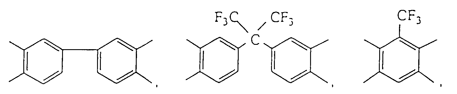
- One aspect of the present invention concerns a waveguide for light transmission therethrough having a core, wherein the core is made of a polyimide obtained from at least one tetracarboxylic dianhydride and at least one diamine, the polyimide being selected from the group consisting of
- the second aspect of the present invention concerns a waveguide having a core for light transmission therethrough, wherein the core is made of a polyimide copolymer including at least two units represented by the formulae [II] and [III] as follows: wherein each of R 1 and R 2 is a tetravalent organic group selected from the group consisting of and with the proviso that R 1 and R 2 are different from each other.
- the third aspect of the present invention concerns a method for making an optical waveguide for light transmission, the optical waveguide having a substrate and at least two stacked layers, first and second layers, formed to cover the substrate, the method comprising the steps of:
- the fourth aspect of the present invention concerns a method for making an optical waveguide for light transmission, the optical waveguide having a substrate and at least two stacked layers, first and second layers, formed to cover the substrate, the method comprising the steps of:
- the optical waveguides thereof are characterized in that the polyimides used to form the core layer and/or the cladding layer are those polyimides having the highest heat resistance.
- These highly heat resistant polyimides can withstand temperatures of 300° C and higher. Accordingly, they are adequately resistant to temperatures generated during soldering of adjacent or nearby electronic components.
- manufacture of long optical waveguides can be easily carried out by use of spin cast methods, thereby permitting manufacture of such optical waveguides at low cost. Because polyimide optical waveguides are generally manufactured at temperatures of 400° C and less, rather than using quartz glass or silicon, prewired multi-use circuit boards made using such polyimides and the like.
- fluorinated polyimide copolymers have been developed, the refractive indices of which are freely controllable, and which can be suitably employed for the manufacture of high quality optical waveguides.
- polyimides which are used to form essential components of the present invention are soluble in certain solvents, they can not be used in conventional methods for the formation of multilayer optical waveguides.
- the present inventors have carried out extensive research concerning the effect of heat treatment at various temperatures on the solubility characteristics of polyimides. As a result, it has been found that upon heat treating suitable polyimides at a predetermined temperature and above, the solubility of the resulting material becomes negligible, thus permitting the fabrication of multilayer polyimide optical waveguides.
- polyimides can be obtained by subjecting poly(amic acid)s which are precursors of the polyimides to heat-treatment up to approximately 300 °C to 350 °C.
- Such the polyimides which are soluble in some solvents can be changed to be insoluble in the solvents by subjecting poly(amic acid)s to heat-treatment at a temperature in the range of 350°C - 380°C.
- the obtained optical waveguide has high optical loss due to thermal decomposition of the polyimides. Therefore, the heat-treatment is carried out at a maximum temperature of 380 °C in order to obtain an optical waveguide having a low optical loss.
- the present inventors have developed a manufacturing method for polyimide optical waveguides, wherein over a layer of organic solvent soluble polyimide, another layer is formed by applying a solution of a poly(amic acid) dissolved in an organic solvent in which the polyimide of the underlying layer is not soluble, thus further facilitating the manufacture of multilayer optical waveguides.
- the employed polyimides include polyimide homopolymers derived from 2,2′-bis(trifluoromethyl)-4,4′-diaminobiphenyl, polyimide copolymers derived from at least one diamine including 2,2′-bis(trifluoromethyl)-4,4′-diaminobiphenyl, and a mixture of the polyimide homopolymers, as described above.
- 2,2′-bis(trifluoromethyl)-4,4′-diaminobiphenyl which is a necessary component of the present invention, is prepared, for example, by the process disclosed in the Journal of Japanese Chemical Society, vol 3, 675 - 676 (1972).
- a tetracarboxylic dianhydride used in the present invention includes pyromellitic dianhydride; 3,3′,4,4′-benzophenonetetracarboxylic dianhydride; 3,3′,4,4′-biphenyletetracarboxylic dianhydride; 2,2-bis(3,4-dicarboxyphenyl)hexafluoropropane dianhydride; trifluoromethylpyromellic dianhydride; 1,4-di(trifluoromethyl)pyromellic dianhydride; 1,4-di(pentafluoroethyl)pyromellic dianhydride; heptafluoropropylpyromellic dianhydride; or the like.
- Japanese Patent Application No. 63-165056 discloses a method for preparing a fluorine-containing anhydride of pyromellitic acid, which has a benzene ring having at least one fluoro-alkyl group, such as trifluoromethylpyromellic dianhydride; 1,4-di(trifluoromethyl)pyromellic dianhydride; 1,4-di(pentafluoroethyl)pyromellic dianhydride; heptafluoropropylpyromellic dianhydride; or the like.
- a copolymer of poly(amic acid) is synthesized by reacting the diamine mentioned above with two kinds of tetracarboxylic dianhydrides.
- the tetracarboxylic dianhydrides used in the synthesis of the poly(amic acid)s may be replaced with the tetracarboxylic acids, the tetracarboxylic acid chlorides, or esters of the tetracarboxylic acids.
- a polyimide copolymer may be prepared by reacting the diamines with at least three kinds of tetracarboxylic anhydrides in order to control easily and precisely the refractive index of a waveguide.
- a polyimide is derived from only one poly(amic acid) and a mixture of polyimides may be derived from a mixture of at least two poly(amic acid)s.
- the polyimides used in the present invention include not only a polyimide homopolymer derived from 2,2′-bis(trifluoromethyl)-4,4′-diaminobiphenyl and a tetracarboxylic dianhidride but also a polyimide copolymer derived from 2,2′-bis(trifluoromethyl)-4,4′-diaminobiphenyl and a mixture including the polyimide homopolymers.
- the monomers (diamines or dianhidrides) listed below may be used with 2,2′-bis(trifluoromethyl)-4,4′-diaminobiphenyl and the tetracarboxylic dianhidride.
- Such compatible diamines include m-phenylenediamine
- Such the compatible dianhydrides include
- optical waveguides of the present invention many of the well known different types of optical waveguides can be fabricated, including fiber type, parallel surface type, ridge type, lens type, and embedded type optical waveguides.
- the core - cladding refractive index ratio of these optical waveguides can be freely controlled so as to achieve wavelength dependent properties thereof which best suit the conditions and requirements under which they will be used.
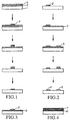
- FIG. 1 illustrates one example of a manufacturing method for ridge type optical waveguides in accordance with the present invention, wherein a substrate 1, core layer 2, aluminum layer 3 and resist layer 4 can be seen.
- a substrate 1 which can be fabricated from silicon and the like.
- a layer of a poly(amic acid) which can be a precursor of a polyimide of the present invention is applied at a specified thickness.
- the previously applied poly(amic acid) is transformed into the above mentioned core layer 2.
- the above mentioned aluminum layer 3 is formed over the core layer 2 using a vapor deposition method, after which resist is applied thereover.
- the ridge type optical waveguide thus obtained therefore is made up of a lower cladding layer consisting of the above mentioned substrate 1 made of silicon or the like, a core layer derived from core layer 2 which is formed from one of the polyimides which characterize the present invention, and an overlying air layer which acts as an upper cladding layer.
- Fig. 2 illustrates another example of a manufacturing method for ridge type optical waveguides in accordance with the present invention, wherein over an optical waveguide of the type prepared by the example shown in Fig. 1, a core layer 5 is formed which consists of a different polyimide of the present invention from that which forms the core layer 2.
- Fig. 3 illustrates another example of a manufacturing method for ridge type optical waveguides in accordance with the present invention, wherein the polyimide layer having an index of refraction lower than the of the above described core layer 2 is first applied over substrate 1, after which steps identical to those of the example shown in Fig. 1 are carried out, starting with formation of the core layer 2 over the polyamide layer first applied over the substrate 1.
- a ridge type optical waveguide is fabricated having a lower cladding layer 6 consisting of the polyimide layer first applied over substrate 1, a core layer derived from the core layer 2, and an overlying air layer which acts as an upper cladding layer.
- Fig. 4 illustrates yet another example of a manufacturing method for embedded type optical waveguides in accordance with the present invention, wherein starting with an optical,waveguide of the type prepared by the example shown in Fig. 3, an upper cladding layer 7 is formed thereover which consists of a polyimide layer which has a lower index of refraction than that of the core layer 2.
- the decomposition temperature and refractive index are shown in Tables 1-1 and 1-2 for a number of polyimide homopolymers, polyimide copolymers, and mixtures of polyimide homopolymers used in the present invention.
- the listed values for decomposition temperature were obtained under a flowing nitrogen atmosphere with the temperature of the sample raising at a rate of 10°C/min., and represent the temperature resulting in a 10 wt % loss in the amount of polyimides studied under the above conditions.
- Refractive indices were measured using an abbe type refractometer at 20°C at a wavelength of 589 nm.
- Optical waveguides were prepared using the polyimide homopolymers, polyimide copolymers, and mixtures of the polyimide homopolymers shown in Tables 1-1 and 1-2. Optical losses in each were measured at wavelengths of 0.63 ⁇ m and 1.3 ⁇ m by means of the streak light scattering method and cutback method.
- heat treatment was carried out at 70°C for 2 hours; at 160°C for 1 hour; at 250°C for 30 minutes, and at 350°C for 1 hour.
- the result measurement of the photopropagation loss of the obtained waveguide using a streak light scattering method with light having a wavelength of 0.63 ⁇ m was 0.9 dB/cm.
- a parallel-surface-type optical waveguide having a lower cladding layer of a silicon oxide layer, a core layer of polyimide copolymer 11 in Table 1-1, and an upper cladding layer of an overlying air layer was obtained by repeating the same procedures as described in Example 1 except that a solution of a poly(amic acid), which is a precursor of polyimide copolymer 11 in Table 1-1, in an amount of 10 % by weight in DMA was used instead of a solution of the poly(amic acid), which is the precursor of polyimide homopolymer 1 in Table 1-1, in an amount of 10 % by weight in DMA.
- the result measurement of the photopropagation loss of the obtained optical waveguide using a streak light scattering method with light having a wavelength of 0.63 ⁇ m was 0.7 dB/cm.
- a parallel-surface-type optical waveguide having a lower cladding layer of a silicon oxide layer; a core layer of polyimide homopolymer 4 in Table 1-1, and an upper cladding layer of an overlying air layer was obtained by repeating the same procedures as described in Example 1 except that a solution of a poly(amic acid), which is a precursor of polyimide homopolymer 4 in Table 1-1, in an amount of 10 % by weight in DMA was used instead of the solution of the poly(amic acid), which is the precursor of polyimide homopolymer 1 in Table 1-1, in an amount of 10 % by weight in DMA.
- the result measurement of the photopropagation loss of the obtained optical waveguide measured by a streak light scattering method with light having a wavelength of 0.63 ⁇ m was 0.5 dB/cm.
- a solution of a poly(amic acid), which is a precursor of polyimide copolymer 16 in Table 1-1, in an amount of 10 a by weight in DMA was cast on a silicon wafer 3 inches in diameter having an silicon oxide surface layer by a spin cast method and was subjected to heat-treatment up to a maximum temperature of 350°C (in detail, heat treatment was carried out at 70°C for 2 hours; at 160°C for 1 hour; at 250°C for 30 minutes, and at 350°C for 1 hour) so that the heat-treated wafer had a 30 ⁇ m thick layer of polyimide copolymer 16, thus forming a lower cladding layer.
- a solution of a poly(amic acid), which is a precursor of polyimide homopolymer 1 in Table 1-1, in an amount of 10 % by weight in DMA was cast on the lower cladding layer by a spin cast method and the coated lower cladding layer was subjected to heat-treatment up to a maximum temperature of 350°C (in detail, heat treatment was carried out at 70°C for 2 hours; at 160°C for 1 hour; at 250°C for 30 minutes, and at 350°C for 1 hour) so that the heat-treated lower cladding layer had a 10 ⁇ m thick layer of polyimide homopolymer 1, thus forming a core layer on the lower cladding layer.
- the core layer cast by the aluminum was subjected to resist processing.
- a usual positive-type resist was formed on the processed layer of the wafer by a spin cast method and subsequently prebaked at approximately 95°C.
- the resist layer was then exposed to ultraviolet radiation through a mask for forming a pattern having a line width of 10 ⁇ m and a length of 60 mm by the use of an ultra-high pressure mercury vapor lamp, and subsequently developed with a developer for a positive-type resist.
- the developed layer was after-baked at 135 °C.
- the aluminum parts which were not coated by the resist were subjected to wet etching.
- the polyimide of the wafer was subjected to reactive ion etching (RIE) processing.
- RIE reactive ion etching
- the aluminum layer formed on the polyimide layer was removed by the etching agent mentioned above, thus obtaining a ridge-type optical waveguide having a lower cladding layer of polyimide copolymer 16 in Table 1-1, a core layer of polyimide homopolymer 1 in Table 1-1, and an upper cladding of an overlying air layer.
- the result measurement of the photopropagation loss of the obtained optical waveguide using a cutback method with light having a wavelength of 1.3 ⁇ m was 0.3 dB/cm.
- a ridge-type waveguide having a lower cladding layer of polyimide homopolymer 4 in Table 1-1, a core layer of polyimide copolymer 7 in Table 1-1, and an upper cladding layer of an overlying air layer was obtained by repeating the same procedures as described in Example 4 except that a solution of a poly(amic acid), which is a precursor of polyimide homopolymer 4 in Table 1-1, in an amount of 10 % by weight in DMA was used in the cladding layer instead of the solution of the poly(amic acid), which is the precursor of polyimide copolymer 16 in Table 1-1, in an amount of 10 % by weight in DMA; that a solution of a poly(amic acid), which is a precursor of polyimide copolymer 7 in Table 1-1, in an amount of 10 % by weight in DMA was used in the core layer instead of the solution of the poly(amic acid), which is the precursor of polyimide homopolymer 1 in Table 1-1, in an amount of
- the heat-treatment was carried out at 70°C for 2 hours; at 160°C for 1 hour; at 250°C for 30 minutes, and at 380°C for 1 hour.
- the result measurement of the photopropagation loss of the obtained optical waveguide using a cutback method with light having a wavelength of 1.3 ⁇ m was 0.3 dB/cm.
- a ridge-type waveguide having a lower cladding layer of polyimide homopolymer 4 in Table 1-1, a core layer of polyimide copolymer 7 in Table 1-1, and an upper cladding layer of an overlying air layer was obtained by repeating the same procedures as described in Example 5 except that a solution of a poly(amic acid), which is a precursor of polyimide copolymer 7 in Table 1-1, in an amount of 10 a by weight in n-hexanol, was used in the core layer instead of the solution of the poly(amic acid), which is the precursor of polyimide copolymer 7 in Table 1-1, in an amount of 10 % by weight in DMA; and that the maximum temperature of heat-treatment to the poly(amic acid), being the precursor of polyimide homopolymer 4 in Table 1-1 to be the lower cladding was 350°C instead of 380°C.
- the heat-treatment was carried out at 70°C for 2 hours; at 160°C for 1 hour; at 250°C for 30 minutes, and at 350°C for 1 hour.
- the result measurement of the photopropagation loss of the obtained optical waveguide using a cutback method with light having a wavelength of 1.3 ⁇ m was 0.3 dB/cm.
- a ridge-type waveguide having a lower cladding layer of polyimide copolymer 10 in Table 1-1, a core layer of polyimide copolymer 11 in Table 1-1, and an upper cladding layer of an overlying air layer was obtained by repeating the same procedures as described in Example 5 except that a solution of a poly(amic acid), which is a precursor of polyimide copolymer 10 in Table 1-1, in an amount of 10 % by weight in DMA, was used in the lower cladding layer instead of the solution of the poly(amic acid), which is the precursor of polyimide homopolymer 4 in Table 1-1, in an amount of 10 % by weight in DMA; and that a solution of a poly(amic acid), which is a precursor of polyimide copolymer 11 in Table 1-1, in an amount of 10 % by weight in DMA, was used in the core layer instead of the solution of the poly(amic acid), which is the precursor of polyimide copolymer 7 in Table 1-1,
- the maximum temperature of heat-treatment to the poly(amic acid), being the precursor of polyimide copolymer 10 in Table 1-1 to be the lower cladding layer was 380°C.
- the heat-treatment was carried out at 70°C for 2 hours; at 160°C for 1 hour; at 250°C for 30 minutes, and at 380°C for 1 hour.
- the result measurement of the photopropagation loss of the obtained waveguide using a cutback method with light having a wavelength of 1.3 ⁇ m was 0.3 dB/cm.
- a ridge-type waveguide having a lower cladding layer of polyimide copolymer 10 in Table 1-1, a core layer of polyimide copolymer 11 in Table 1-1, and an upper cladding layer of an overlying air layer was obtained by repeating the same procedures as described in Example 7 except that a solution of a poly(amic acid), which is a precursor of polyimide copolymer 10 in Table 1-1, in an amount of 10 % by weight in n-hexanol, was used in the lower cladding layer instead of the solution of the poly(amic acid), which is the precursor of polyimide copolymer 10 in Table 1-1, in an amount of 10 % by weight in DMA; and that the maximum temperature of heat-treatment to the poly(amic acid), being the precursor of polyimide copolymer 10 in Table 1-1 to be the lower cladding was 350°C instead of 380°C.
- the heat-treatment was carried out at 70°C for 2 hours; at 160°C for 1 hour; at 250°C for 30 minutes, and at 350°C for 1 hour.
- the result measurement of the photopropagation loss of the obtained optical waveguide using a cutback method with light having a wavelength of 1.3 ⁇ m was 0.3 dB/cm.
- Each layer of the obtained optical waveguide was composed of the polyimide according to the present invention.
- the result measurement of the photopropagation loss of the obtained optical waveguide using a cutback method with light having a wavelength of 1.3 ⁇ m was 0.1 dB/cm.
- Each layer of the obtained waveguide was composed of the polyimide according to the present invention.
- the result measurement of the photopropagation loss of the obtained optical waveguide using a cutback method with light having a wavelength of 1.3 ⁇ m was 0.1 dB/cm.
- Each layer of the obtained optical waveguide was composed of the polyimide according to the present invention.
- the result measurement of the photopropagation loss of the obtained optical waveguide using a cutback method with light having a wavelength of 1.3 ⁇ m was 0.1 dB/cm.
- the core layer coated by the aluminum was subjected to resist processing.
- a usual positive-type resist was formed on the processed layer of the wafer by a spin-coat method and subsequently prebaked at approximately 95 °C.
- the resist layer was then exposed to ultraviolet radiation through a mask for forming a pattern having a line width of 10 ⁇ m and a length of 60 mm by the use of an ultra-high pressure mercury vapor lamp, and subsequently developed with a developer for a positive-type resist.
- the developed layer was after-baked at 135 °C.
- the aluminum parts which were not coated by the resist were subjected to wet etching.
- the polyimide (polyimide copolymer 11 in Table 1-1) of the wafer was subjected to RIE processing.
- the aluminum layer formed on the polyimide layer was removed by the etching agent mentioned above, thus obtaining a first ridge-type waveguide having a core layer of polyimide copolymer 11 in Table 1-1, and an upper cladding layer of an overlying air layer.
- a solution of a poly(amic acid), which is a precursor of polyimide homopolymer 4 in Table 1-1, in an amount of 10 % by weight in DMA was cast on the first ridge-type optical waveguide obtained above by a spin cast method and was subjected to heat-treatment up to a maximum temperature of 380 °C (in detail, the heat treatment was carried out at 70 °C for 2 hours; at 160 °C for 1 hour; at 250 °C for 30 minutes, and at 380 °C for 1 hour) so that the heat-treated wafer had a 10 ⁇ m thick layer of polyimide copolymer 4, thus forming another core layer.
- a second ridge type optical waveguide was formed by repeating the same procedures as described in the method for preparing the first ridge-type optical waveguide mentioned above, thus obtaining two kinds of optical waveguides, having different refractive index each other, formed on the same substrate, wherein one optical waveguide had the core layer of polyimide 11 in Table 1-1 and the other optical waveguide had the core layer of polyimide homopolymer 4 in Table 1-1.
- the result measurements of the photopropagation loss of the obtained two kinds of optical waveguides, the first optical waveguide and the second optical waveguide, using a cutback method with light having a wavelength of 1.3 ⁇ m were 0.3 dB/cm and 0.3 dB/cm.
- a solution of a poly(amic acid), which is a precursor of polyimide copolymer 11 in Table 1-1, in an amount of 10 % by weight in DMA was cast on a silicon wafer 3 inches in diameter having an silicon oxide surface layer by a spin-cast method and the cast wafer was subjected to heat-treatment up to a maximum temperature of 350 °C (in detail, the heat treatment was carried out at 70 °C for 2 hours; at 160 °C for 1 hour; at 250 °C for 30 minutes, and at 350 °C for 1 hour) so that the heat-treated wafer had a 10 ⁇ m thick layer of polyimide copolymer 11, thus forming a core layer.
- the core layer cast by the aluminum was subjected to resist processing.
- a usual positive-type resist was formed on the processed layer of the wafer by a spin cast method and subsequently prebaked at approximately 95 °C.
- the resist layer was then exposed to ultraviolet radiation through a mask for forming a pattern having a line width of 10 ⁇ m and a length of 60 mm by the use of an extra-high pressure mercury vapor lamp, and subsequently developed with a developer for a positive-type resist.
- the developed layer was after-baked at 135 °C.
- the aluminum parts which were not coated by the resist were subjected to a wet etching.
- the polyimide (polyimide copolymer 11 in Table 1-1) of the wafer was subjected to a RIE processing.
- the aluminum layer formed on the polyimide layer was removed by the etching agent mentioned above, thus obtaining a first ridge-type waveguide having a core layer of polyimide copolymer 11 in Table 1, and an upper cladding part of an overlying air layer.
- a solution of a poly(amic acid), which is a precursor of polyimide homopolymer 4 in Table 1-1, in an amount of 10 % by weight in n-hexanol was cast on the first ridge-type optical waveguide obtained above by a spin cast method and was subjected to heat-treatment up to a maximum temperature of 350 °C (in detail, the heat treatment was carried out at 70 °C for 2 hours; at 160 °C for 1 hour; at 250 °C for 30 minutes, and at 350 °C for 1 hour) so that the heat-treated wafer had a 10 ⁇ m thick layer of polyimide homopolymer 4, thus forming another core layer.
- a second ridge type optical waveguide was formed by repeating the same procedures as described in the method for preparing the first ridge-type optical waveguide mentioned above, thus obtaining two kinds of optical waveguides, having different refractive index each other, formed on the same substrate, wherein one optical waveguide had the core layer of polyimide 11 in Table 1-1 and the other optical waveguide had the core layer of polyimide homopolymer 4 in Table 1-1.
- the result measurements of the photopropagation loss of the obtained two kinds of optical waveguides, the first optical waveguide and the second optical waveguide, using a cutback method with light having a wavelength of 1.3 ⁇ m were 0.3 dB/cm and 0.3 dB/cm.
- a ridge-type optical waveguide having a lower cladding layer of polyimide homopolymer 4 in Table 1-1, a core layer of polyimide copolymer 7 in Table 1-1, and an upper cladding layer of an overlying air layer obtained by repeating the same procedures as described in Example 5 except that the maximum temperature of heat-treatment to the poly(amic acid), being the precursor of polyimide homopolymer 4 in Table 1-1 to be the lower cladding was 350 °C.
- the heat-treatment was carried out at 70 °C for 2 hours; at 160 °C for 1 hour; at 250 °C for 30 minutes, and at 350 °C for 1 hour.
- an optical waveguide which has properties including low optical losses, facile fabrication, controllrable core - cladding refractive index, and high heat resistance can be provided.
- the core - cladding refractive index ratio which has not been obtained in conventional quartz glass optical waveguides and plastic optical waveguides can be freely controlled according to the present invention.
Landscapes
- Chemical & Material Sciences (AREA)
- Chemical Kinetics & Catalysis (AREA)
- Medicinal Chemistry (AREA)
- Polymers & Plastics (AREA)
- Organic Chemistry (AREA)
- Health & Medical Sciences (AREA)
- Physics & Mathematics (AREA)
- Engineering & Computer Science (AREA)
- Microelectronics & Electronic Packaging (AREA)
- General Physics & Mathematics (AREA)
- Optics & Photonics (AREA)
- Optical Integrated Circuits (AREA)
- Macromolecular Compounds Obtained By Forming Nitrogen-Containing Linkages In General (AREA)
Claims (4)
- Guide d'onde optique pour la transmission de lumière à travers celui-ci, comportant un noyau, le noyau étant fait en un polyimide obtenu à partir d'au moins un dianhydride d'acide tétracarboxylique et d'au moins une diamine, le polyimide étant choisi dans le groupe constitué de :(a) un homopolymère polyimide dérivé d'une diamine représentée par la formule [I] suivante :
 (b) un copolymère polyimide dérivé d'au moins une diamine comprenant la diamine représentée par la formule [I] ;(c) un mélange des homopolymères polyimide.
 - Guide d'onde optique comportant un noyau pour la transmission de lumière à travers celui-ci, le noyau étant fait en un copolymère polyimide comprenant au moins deux motifs représentés par les formules [II] et [III] suivantes :


à la condition que R1 et R2 soient différents l'un de l'autre. - Procédé de fabrication d'un guide d'onde optique pour la transmission de lumière, le guide d'onde optique comportant un substrat et au moins deux couches superposées, première et deuxième couches, formées de façon à recouvrir le substrat, le procédé comprenant les étapes consistant :(a) à préparer un substrat et au moins deux types de solutions, au moins l'une de celles-ci étant une solution d'un acide polyamique qui est un précurseur d'un polyimide, le polyimide étant choisi dans le groupe constitué par :(1) un homopolymère polyimide dérivé d'une diamine représentée par la formule [I] suivante :
 (2) un copolymère polyimide dérivé d'au moins une diamine comprenant la diamine représentée par la formule [I] ;(3) un mélange des homopolymères polyimide ;(b) à former une couche d'une solution parmi lesdits au moins deux types de solutions sur le substrat ;(c) à soumettre la couche de la solution à un traitement thermique à une température dans l'intervalle de 350 °C à 380 °C afin de solidifier la couche de la solution pour former une première couche ;(d) à former une couche de l'autre solution choisie parmi lesdits au moins deux types de solutions sur la première couche, la première couche étant insoluble dans l'autre solution ;(e) à soumettre la couche de l'autre solution à un traitement thermique à une température dans l'intervalle de 350 °C à 380 °C afin de solidifier la couche de l'autre solution pour former une deuxième couche.
 - Procédé de fabrication d'un guide d'onde optique pour la transmission de lumière, le guide d'onde optique comportant un substrat et au moins deux couches superposées, première et deuxième couches formées de façon à recouvrir le substrat, le procédé comprenant les étapes consistant :(a) à préparer un substrat et au moins deux types de solutions, au moins l'une de celles-ci étant une solution d'un acide polyamique qui est un précurseur d'un copolymère polyimide comprenant au moins deux motifs représentés par les formules [II] et [III] suivantes :


à la condition que R1 et R2 soient différents l'un de l'autre ;(b) à former une couche d'une solution choisie parmi lesdits au moins deux types de solutions sur le substrat ;(c) à soumettre la couche de la solution à un traitement thermique à une température dans l'intervalle de 350 °C à 380 °C afin de solidifier la couche de la solution pour former une première couche ;(d) à former une couche de l'autre solution choisie parmi lesdits au moins deux types de solutions sur la première couche, la première couche étant insoluble dans l'autre solution ;(e) à soumettre la couche de l'autre solution à un traitement thermique à une température dans l'intervalle de 350 °C à 380 °C afin de solidifier la couche de l'autre solution et former une deuxième couche.
Applications Claiming Priority (8)
| Application Number | Priority Date | Filing Date | Title |
|---|---|---|---|
| JP11050090A JP2813713B2 (ja) | 1990-04-27 | 1990-04-27 | ポリイミド系光導波路 |
| JP110500/90 | 1990-04-27 | ||
| JP110498/90 | 1990-04-27 | ||
| JP11049890A JP2640553B2 (ja) | 1990-04-27 | 1990-04-27 | フッ素化ポリイミド共重合体及びその製造方法 |
| JP12572/91 | 1991-01-11 | ||
| JP1257191A JP2816770B2 (ja) | 1991-01-11 | 1991-01-11 | ポリイミド光導波路の製造方法 |
| JP12571/91 | 1991-01-11 | ||
| JP1257291A JP2816771B2 (ja) | 1991-01-11 | 1991-01-11 | ポリイミド光導波路及びその製造方法 |
Publications (3)
| Publication Number | Publication Date |
|---|---|
| EP0454590A2 EP0454590A2 (fr) | 1991-10-30 |
| EP0454590A3 EP0454590A3 (en) | 1993-02-24 |
| EP0454590B1 true EP0454590B1 (fr) | 1996-06-26 |
Family
ID=27455837
Family Applications (1)
| Application Number | Title | Priority Date | Filing Date |
|---|---|---|---|
| EP91401120A Expired - Lifetime EP0454590B1 (fr) | 1990-04-27 | 1991-04-26 | Guide d'onde optique à partir de polyimide |
Country Status (4)
| Country | Link |
|---|---|
| US (1) | US5108201A (fr) |
| EP (1) | EP0454590B1 (fr) |
| CA (1) | CA2041133C (fr) |
| DE (1) | DE69120464T2 (fr) |
Cited By (1)
| Publication number | Priority date | Publication date | Assignee | Title |
|---|---|---|---|---|
| US7058249B2 (en) | 2001-10-16 | 2006-06-06 | Lightwave Microsystems Corporation | Waveplate and optical circuit formed using mesogen-containing polymer |
Families Citing this family (50)
| Publication number | Priority date | Publication date | Assignee | Title |
|---|---|---|---|---|
| DE3927498C2 (de) * | 1989-08-21 | 2002-01-17 | Merck Patent Gmbh | Polyamidester, Verfahren zu ihrer Herstellung und ihre Verwendung zur Herstellung von Polyimiden |
| US5234772A (en) * | 1990-02-13 | 1993-08-10 | Nippon Telegraph And Telephone Corporation | Dielectric multilayer, filter, manufacturing method therefor, and optical element incorporating the same |
| JPH0641305A (ja) * | 1991-10-25 | 1994-02-15 | Internatl Business Mach Corp <Ibm> | フッ素化された反応体からのポリアミド酸およびポリイミド |
| US5917980A (en) * | 1992-03-06 | 1999-06-29 | Fujitsu Limited | Optical circuit device, its manufacturing process and a multilayer optical circuit using said optical circuit device |
| US5818983A (en) * | 1992-03-06 | 1998-10-06 | Fujitsu Limited | Optical integrated circuit, optical circuit waveguide device and process for oriented, selective growth and formation of organic film |
| SE470147B (sv) * | 1992-04-16 | 1993-11-15 | Ericsson Telefon Ab L M | Inkapsling för optisk vågledare |
| US5265177A (en) * | 1992-05-08 | 1993-11-23 | At&T Bell Laboratories | Integrated optical package for coupling optical fibers to devices with asymmetric light beams |
| US5324813A (en) * | 1992-07-22 | 1994-06-28 | International Business Machines Corporation | Low dielectric constant fluorinated polymers and methods of fabrication thereof |
| US5317657A (en) * | 1992-07-30 | 1994-05-31 | International Business Machines Corporation | Extrusion of polymer waveguides onto surfaces |
| US5317082A (en) * | 1992-12-22 | 1994-05-31 | Amoco Corporation | Photodefinable optical waveguides |
| DE69434548T2 (de) * | 1993-03-18 | 2006-08-03 | Nippon Telegraph And Telephone Corp. | Herstellungsverfahren eines polyimiden optischen wellenleiters |
| US5609797A (en) * | 1993-05-03 | 1997-03-11 | The Boeing Company | Method for recording refractive index patterns in polyimide films |
| JP3501235B2 (ja) * | 1993-05-07 | 2004-03-02 | 日本電信電話株式会社 | 導波型光デバイス |
| JPH08184718A (ja) * | 1994-12-28 | 1996-07-16 | Hoechst Japan Ltd | 光導波路素子およびその製造方法 |
| US5649045A (en) * | 1995-12-13 | 1997-07-15 | Amoco Corporation | Polymide optical waveguide structures |
| US5793046A (en) * | 1996-10-23 | 1998-08-11 | Mcdermott Technology, Inc. | Active cladding scintillating-fiber radiation detector |
| JPH10221549A (ja) * | 1997-02-07 | 1998-08-21 | Hitachi Ltd | プラスチック製光導波路およびそれを用いた光スイッチ |
| US6229949B1 (en) * | 1997-02-19 | 2001-05-08 | Hitachi, Ltd. | Polymer optical waveguide, optical integrated circuit, optical module and optical communication apparatus |
| US6599631B2 (en) * | 2001-01-26 | 2003-07-29 | Nanogram Corporation | Polymer-inorganic particle composites |
| US7226966B2 (en) * | 2001-08-03 | 2007-06-05 | Nanogram Corporation | Structures incorporating polymer-inorganic particle blends |
| KR100248055B1 (ko) * | 1997-08-26 | 2000-03-15 | 윤종용 | 하이브리드 광도파로 및 그 제작 공정 |
| CN1122186C (zh) * | 1997-11-05 | 2003-09-24 | 三星电子株式会社 | 聚合物光波导器件及其制造方法 |
| KR100310092B1 (ko) * | 1998-11-18 | 2001-11-07 | 윤종용 | 광통신용 폴리이미드, 그 제조방법 및 그것을 이용한 다층 폴리이미드막의 형성방법 |
| JP2000162460A (ja) * | 1998-11-27 | 2000-06-16 | Sharp Corp | 有機光導波路およびその製造方法並びにそれを用いた光学部品 |
| JP2000347054A (ja) * | 1999-03-31 | 2000-12-15 | Sharp Corp | 光デバイス及びその製造方法、並びに、ポリイミド膜の製造方法 |
| KR100319299B1 (ko) * | 1999-04-14 | 2002-01-05 | 윤종용 | 광통신용 폴리이미드 |
| JP2002060490A (ja) * | 1999-12-10 | 2002-02-26 | Nitto Denko Corp | ポリアミド酸とそれより得られるポリイミド樹脂とそれらの回路基板への利用 |
| US6690852B2 (en) | 2000-06-22 | 2004-02-10 | Fujikura Ltd. | Optical multiplexer/demultiplexer |
| US20030064235A1 (en) * | 2000-08-09 | 2003-04-03 | Yuichi Okawa | Optical members made of polymide resins |
| JP2002090559A (ja) * | 2000-09-13 | 2002-03-27 | Minolta Co Ltd | ポリイミド光導波路 |
| DE60008121T2 (de) * | 2000-11-28 | 2004-09-16 | National University Of Ireland, Cork | Herstellung von Materialien für Wellenleiter mit Stufenbrechungsindex |
| JP2004514941A (ja) | 2000-11-28 | 2004-05-20 | フォトン−エックス インコーポレイテッド | 薄膜光ウエーブガイド |
| JP3762677B2 (ja) * | 2001-01-29 | 2006-04-05 | 株式会社 堀場アドバンスドテクノ | 流体分析用セルおよびこれを用いた分析装置 |
| US7026634B2 (en) * | 2001-06-28 | 2006-04-11 | E-Beam & Light, Inc. | Method and apparatus for forming optical materials and devices |
| US6751396B2 (en) * | 2001-12-26 | 2004-06-15 | Lucent Technologies Inc. | Integrated optical devices and method of fabrication therefor |
| US7274854B2 (en) | 2002-06-27 | 2007-09-25 | Pirelli & C. S.P.A. | Polyimide optical waveguides and method for the preparation thereof |
| US7280731B2 (en) * | 2002-07-05 | 2007-10-09 | Silecs Oy | Stable organic-inorganic materials for waveguides, optical devices, and other applications |
| JP4181921B2 (ja) * | 2003-05-19 | 2008-11-19 | 日東電工株式会社 | ポリマー光導波路 |
| US7206480B2 (en) * | 2003-08-01 | 2007-04-17 | Bae Systems Information And Electronic Systems Integration Inc. | Method of forming interlayer connections in integrated optical circuits, and devices formed using same |
| US7324723B2 (en) * | 2003-10-06 | 2008-01-29 | Mitsui Chemicals, Inc. | Optical waveguide having specular surface formed by laser beam machining |
| CN1957019A (zh) * | 2004-05-21 | 2007-05-02 | 和光纯药工业株式会社 | 重氢化聚酰亚胺化合物及其衍生物 |
| EP1760114A3 (fr) * | 2005-08-22 | 2008-05-14 | Nippon Shokubai Co., Ltd. | Composition de polyamide-acide et ses applications. |
| JP4679582B2 (ja) * | 2005-08-29 | 2011-04-27 | 三井化学株式会社 | 光導波路フィルムとその製造方法、それを含む光電気混載フィルムおよび電子機器 |
| US7972691B2 (en) * | 2006-12-22 | 2011-07-05 | Nanogram Corporation | Composites of polymers and metal/metalloid oxide nanoparticles and methods for forming these composites |
| WO2008100568A1 (fr) * | 2007-02-17 | 2008-08-21 | Nanogram Corporation | Composites fonctionnels, encres fonctionnelles et applications associées |
| US8314176B2 (en) * | 2009-01-08 | 2012-11-20 | Nanogram Corporation | Composites of polysiloxane polymers and inorganic nanoparticles |
| US8668992B2 (en) | 2011-06-01 | 2014-03-11 | Brewer Science Inc. | Fluorinated polyimides with fluorene cardo structure as optical materials that have low absolute thermo-optic coefficients |
| KR20150023728A (ko) | 2012-06-19 | 2015-03-05 | 신닛테츠 수미킨 가가쿠 가부시키가이샤 | 표시장치 및 그 제조방법, 그리고 표시장치 지지기재용 폴리이미드 필름 및 그 제조방법 |
| KR102433790B1 (ko) * | 2015-07-07 | 2022-08-18 | 삼성디스플레이 주식회사 | 전극, 그 제조 방법 및 이를 포함하는 유기 발광 표시 장치 |
| CN109690373B (zh) * | 2016-07-15 | 2022-06-10 | 康宁股份有限公司 | 具有层叠结构的光波导制品及其形成方法 |
Family Cites Families (9)
| Publication number | Priority date | Publication date | Assignee | Title |
|---|---|---|---|---|
| JP2657700B2 (ja) * | 1988-08-08 | 1997-09-24 | 日本電信電話株式会社 | 含フッ素ポリイミド光学材料 |
| JP2744969B2 (ja) * | 1988-08-26 | 1998-04-28 | 日本電信電話株式会社 | 含フッ素ポリイミド及びその製造方法 |
| US5024506A (en) * | 1989-01-27 | 1991-06-18 | At&T Bell Laboratories | Plenum cables which include non-halogenated plastic materials |
| US4941729A (en) * | 1989-01-27 | 1990-07-17 | At&T Bell Laboratories | Building cables which include non-halogenated plastic materials |
| US5175242A (en) * | 1989-02-24 | 1992-12-29 | The University Of Akron | Phenylated polyimides prepared from 3,6-diarylpyromellitic dianhydride and aromatic diamines |
| JPH0676554B2 (ja) * | 1989-03-27 | 1994-09-28 | 日本電信電話株式会社 | 含フッ素ポリイミド組成物及びその製造方法 |
| US4969706A (en) * | 1989-04-25 | 1990-11-13 | At&T Bell Laboratories | Plenum cable which includes halogenated and non-halogenated plastic materials |
| US5071997A (en) * | 1989-07-20 | 1991-12-10 | University Of Akron | Polyimides comprising substituted benzidines |
| JP2688698B2 (ja) * | 1989-07-31 | 1997-12-10 | 日本電信電話株式会社 | 光学材料用ポリイミドワニス及びその製造方法 |
-
1991
- 1991-04-24 CA CA002041133A patent/CA2041133C/fr not_active Expired - Lifetime
- 1991-04-26 DE DE69120464T patent/DE69120464T2/de not_active Expired - Lifetime
- 1991-04-26 US US07/692,249 patent/US5108201A/en not_active Expired - Lifetime
- 1991-04-26 EP EP91401120A patent/EP0454590B1/fr not_active Expired - Lifetime
Cited By (1)
| Publication number | Priority date | Publication date | Assignee | Title |
|---|---|---|---|---|
| US7058249B2 (en) | 2001-10-16 | 2006-06-06 | Lightwave Microsystems Corporation | Waveplate and optical circuit formed using mesogen-containing polymer |
Also Published As
| Publication number | Publication date |
|---|---|
| EP0454590A3 (en) | 1993-02-24 |
| EP0454590A2 (fr) | 1991-10-30 |
| CA2041133A1 (fr) | 1991-10-28 |
| US5108201A (en) | 1992-04-28 |
| DE69120464T2 (de) | 1997-02-06 |
| DE69120464D1 (de) | 1996-08-01 |
| CA2041133C (fr) | 1995-01-03 |
Similar Documents
| Publication | Publication Date | Title |
|---|---|---|
| EP0454590B1 (fr) | Guide d'onde optique à partir de polyimide | |
| EP0675915B1 (fr) | Guides d'ondes optiques photodefinissables | |
| KR100373892B1 (ko) | 폴리이미드및이를사용하여수득한광학부품 | |
| JPH1112465A (ja) | ポリアミド酸溶液、ポリイミドフィルムおよびポリイミドフィルムの特性制御方法 | |
| US6136929A (en) | Polyarylene ether for optical communication | |
| KR100350412B1 (ko) | 퍼플루오르화 지방족기를 갖는 불소화 폴리에테르 및 이를 사용한 광도파로 | |
| JP3674878B2 (ja) | ポリイミド光導波路 | |
| JP2816771B2 (ja) | ポリイミド光導波路及びその製造方法 | |
| WO2007023997A1 (fr) | Composition de résine de polyamide-acide fluoré pour matériaux optiques | |
| JP3486357B2 (ja) | 光学用ポリイミド基板 | |
| JP2816770B2 (ja) | ポリイミド光導波路の製造方法 | |
| JP3486358B2 (ja) | 光学用ポリイミド基板 | |
| JP2000292635A (ja) | フッ素化ポリイミド樹脂およびそれらを用いた光導波路 | |
| JP2001242334A (ja) | 異形ポリイミド光導波路およびその製造方法 | |
| KR102109931B1 (ko) | 포스포러스계 디아민 화합물, 이로부터 형성된 폴리아믹산과 폴리이미드 및 폴리이미드를 포함한 폴리이미드 필름 | |
| JPH0915608A (ja) | 低複屈折ポリイミド膜の製造方法 | |
| KR100292800B1 (ko) | 불소치환폴리아릴렌에테르공중합체및이를이용한폴리머광소자 | |
| JP3002710B2 (ja) | 低パーティクル含有ポリイミド前駆体およびポリイミド溶液およびその製造法 | |
| JP3702449B2 (ja) | 光部品用ポリイミド前駆体及びこれを用いた光部品 | |
| JP2009269986A (ja) | 高分子−無機ハイブリッド光学材料 | |
| KR102103552B1 (ko) | 칼코겐계 디아민, 이로부터 형성된 폴리아믹산과 폴리이미드, 상기 폴리이미드를 포함한 폴리이미드 필름 | |
| JP2000072876A (ja) | 含フッ素ポリイミド樹脂およびそれらを用いた光導波路 | |
| JP2002202424A (ja) | 高分子光導波路 | |
| JP2002202422A (ja) | 高分子光導波路 | |
| Matsuura et al. | Synthesis and properties of partially fluorinated polyimides for optical applications |
Legal Events
| Date | Code | Title | Description |
|---|---|---|---|
| PUAI | Public reference made under article 153(3) epc to a published international application that has entered the european phase |
Free format text: ORIGINAL CODE: 0009012 |
|
| AK | Designated contracting states |
Kind code of ref document: A2 Designated state(s): DE FR GB |
|
| PUAL | Search report despatched |
Free format text: ORIGINAL CODE: 0009013 |
|
| AK | Designated contracting states |
Kind code of ref document: A3 Designated state(s): DE FR GB |
|
| RIN1 | Information on inventor provided before grant (corrected) |
Inventor name: NISHI, SHIRO Inventor name: SHIMOKAWA, FUSAO Inventor name: KOIKE, SHINJI Inventor name: MATSUURA, TORU Inventor name: SASAKI, SHIGEKUNI Inventor name: ANDO, SHINJI Inventor name: ICHINO, TOSHIHIRO Inventor name: YAMAMOTO, FUMIO |
|
| 17P | Request for examination filed |
Effective date: 19930614 |
|
| 17Q | First examination report despatched |
Effective date: 19950411 |
|
| GRAH | Despatch of communication of intention to grant a patent |
Free format text: ORIGINAL CODE: EPIDOS IGRA |
|
| GRAH | Despatch of communication of intention to grant a patent |
Free format text: ORIGINAL CODE: EPIDOS IGRA |
|
| GRAA | (expected) grant |
Free format text: ORIGINAL CODE: 0009210 |
|
| RAP1 | Party data changed (applicant data changed or rights of an application transferred) |
Owner name: NIPPON TELEGRAPH AND TELEPHONE CORPORATION |
|
| AK | Designated contracting states |
Kind code of ref document: B1 Designated state(s): DE FR GB |
|
| REF | Corresponds to: |
Ref document number: 69120464 Country of ref document: DE Date of ref document: 19960801 |
|
| ET | Fr: translation filed | ||
| PLBE | No opposition filed within time limit |
Free format text: ORIGINAL CODE: 0009261 |
|
| STAA | Information on the status of an ep patent application or granted ep patent |
Free format text: STATUS: NO OPPOSITION FILED WITHIN TIME LIMIT |
|
| 26N | No opposition filed | ||
| REG | Reference to a national code |
Ref country code: GB Ref legal event code: IF02 |
|
| REG | Reference to a national code |
Ref country code: FR Ref legal event code: ST Effective date: 20061230 |
|
| REG | Reference to a national code |
Ref country code: FR Ref legal event code: D3 |
|
| PGFP | Annual fee paid to national office [announced via postgrant information from national office to epo] |
Ref country code: GB Payment date: 20100325 Year of fee payment: 20 |
|
| PGFP | Annual fee paid to national office [announced via postgrant information from national office to epo] |
Ref country code: FR Payment date: 20100521 Year of fee payment: 20 |
|
| PGFP | Annual fee paid to national office [announced via postgrant information from national office to epo] |
Ref country code: DE Payment date: 20100430 Year of fee payment: 20 |
|
| REG | Reference to a national code |
Ref country code: DE Ref legal event code: R071 Ref document number: 69120464 Country of ref document: DE |
|
| REG | Reference to a national code |
Ref country code: GB Ref legal event code: PE20 Expiry date: 20110425 |
|
| PG25 | Lapsed in a contracting state [announced via postgrant information from national office to epo] |
Ref country code: GB Free format text: LAPSE BECAUSE OF EXPIRATION OF PROTECTION Effective date: 20110425 |
|
| PG25 | Lapsed in a contracting state [announced via postgrant information from national office to epo] |
Ref country code: DE Free format text: LAPSE BECAUSE OF EXPIRATION OF PROTECTION Effective date: 20110426 |