EP0443439B1 - Dispositif de mémoire comprenant un transistor et son procédé de fabrication - Google Patents
Dispositif de mémoire comprenant un transistor et son procédé de fabrication Download PDFInfo
- Publication number
- EP0443439B1 EP0443439B1 EP91102082A EP91102082A EP0443439B1 EP 0443439 B1 EP0443439 B1 EP 0443439B1 EP 91102082 A EP91102082 A EP 91102082A EP 91102082 A EP91102082 A EP 91102082A EP 0443439 B1 EP0443439 B1 EP 0443439B1
- Authority
- EP
- European Patent Office
- Prior art keywords
- layer
- storage
- stc
- bitline
- lamella
- Prior art date
- Legal status (The legal status is an assumption and is not a legal conclusion. Google has not performed a legal analysis and makes no representation as to the accuracy of the status listed.)
- Expired - Lifetime
Links
- 238000003860 storage Methods 0.000 title claims abstract description 73
- 238000000034 method Methods 0.000 title claims abstract description 33
- 230000015654 memory Effects 0.000 claims abstract description 40
- 238000004519 manufacturing process Methods 0.000 claims abstract description 15
- 239000003990 capacitor Substances 0.000 claims abstract description 14
- 210000000352 storage cell Anatomy 0.000 claims abstract description 14
- 239000004065 semiconductor Substances 0.000 claims abstract description 13
- 210000004027 cell Anatomy 0.000 claims description 61
- 241000446313 Lamella Species 0.000 claims description 30
- 238000002955 isolation Methods 0.000 claims description 23
- 238000000151 deposition Methods 0.000 claims description 14
- 230000008021 deposition Effects 0.000 claims description 13
- 239000000758 substrate Substances 0.000 claims description 12
- 238000005530 etching Methods 0.000 claims description 9
- 238000004140 cleaning Methods 0.000 claims description 8
- 239000011159 matrix material Substances 0.000 claims description 2
- 230000003647 oxidation Effects 0.000 claims description 2
- 238000007254 oxidation reaction Methods 0.000 claims description 2
- 125000006850 spacer group Chemical group 0.000 claims description 2
- 238000001020 plasma etching Methods 0.000 claims 5
- 230000005669 field effect Effects 0.000 claims 3
- 239000013078 crystal Substances 0.000 claims 1
- 230000003247 decreasing effect Effects 0.000 claims 1
- 238000005137 deposition process Methods 0.000 claims 1
- 238000002360 preparation method Methods 0.000 claims 1
- 238000012876 topography Methods 0.000 claims 1
- 238000009413 insulation Methods 0.000 abstract description 31
- 229910021420 polycrystalline silicon Inorganic materials 0.000 description 25
- 229920005591 polysilicon Polymers 0.000 description 25
- VYPSYNLAJGMNEJ-UHFFFAOYSA-N Silicium dioxide Chemical compound O=[Si]=O VYPSYNLAJGMNEJ-UHFFFAOYSA-N 0.000 description 10
- XUIMIQQOPSSXEZ-UHFFFAOYSA-N Silicon Chemical compound [Si] XUIMIQQOPSSXEZ-UHFFFAOYSA-N 0.000 description 6
- 229910052710 silicon Inorganic materials 0.000 description 6
- 239000010703 silicon Substances 0.000 description 6
- 238000010276 construction Methods 0.000 description 5
- 239000012212 insulator Substances 0.000 description 5
- 235000012239 silicon dioxide Nutrition 0.000 description 5
- 239000000377 silicon dioxide Substances 0.000 description 5
- 238000001039 wet etching Methods 0.000 description 4
- 229910052581 Si3N4 Inorganic materials 0.000 description 2
- 238000000576 coating method Methods 0.000 description 2
- 230000007547 defect Effects 0.000 description 2
- 239000007788 liquid Substances 0.000 description 2
- HQVNEWCFYHHQES-UHFFFAOYSA-N silicon nitride Chemical compound N12[Si]34N5[Si]62N3[Si]51N64 HQVNEWCFYHHQES-UHFFFAOYSA-N 0.000 description 2
- 239000000126 substance Substances 0.000 description 2
- 230000002411 adverse Effects 0.000 description 1
- 230000015572 biosynthetic process Effects 0.000 description 1
- 229910021419 crystalline silicon Inorganic materials 0.000 description 1
- 230000001419 dependent effect Effects 0.000 description 1
- 238000011161 development Methods 0.000 description 1
- 230000018109 developmental process Effects 0.000 description 1
- 238000005516 engineering process Methods 0.000 description 1
- 230000002349 favourable effect Effects 0.000 description 1
- 230000036039 immunity Effects 0.000 description 1
- 230000010354 integration Effects 0.000 description 1
- 230000003993 interaction Effects 0.000 description 1
- 238000004518 low pressure chemical vapour deposition Methods 0.000 description 1
- 238000012856 packing Methods 0.000 description 1
- 238000010405 reoxidation reaction Methods 0.000 description 1
- 238000000926 separation method Methods 0.000 description 1
- 238000004381 surface treatment Methods 0.000 description 1
- 230000008646 thermal stress Effects 0.000 description 1
Images


Classifications
-
- H—ELECTRICITY
- H01—ELECTRIC ELEMENTS
- H01L—SEMICONDUCTOR DEVICES NOT COVERED BY CLASS H10
- H01L23/00—Details of semiconductor or other solid state devices
- H01L23/52—Arrangements for conducting electric current within the device in operation from one component to another, i.e. interconnections, e.g. wires, lead frames
- H01L23/522—Arrangements for conducting electric current within the device in operation from one component to another, i.e. interconnections, e.g. wires, lead frames including external interconnections consisting of a multilayer structure of conductive and insulating layers inseparably formed on the semiconductor body
- H01L23/5226—Via connections in a multilevel interconnection structure
-
- H—ELECTRICITY
- H10—SEMICONDUCTOR DEVICES; ELECTRIC SOLID-STATE DEVICES NOT OTHERWISE PROVIDED FOR
- H10B—ELECTRONIC MEMORY DEVICES
- H10B12/00—Dynamic random access memory [DRAM] devices
- H10B12/01—Manufacture or treatment
- H10B12/02—Manufacture or treatment for one transistor one-capacitor [1T-1C] memory cells
- H10B12/03—Making the capacitor or connections thereto
- H10B12/033—Making the capacitor or connections thereto the capacitor extending over the transistor
-
- H—ELECTRICITY
- H10—SEMICONDUCTOR DEVICES; ELECTRIC SOLID-STATE DEVICES NOT OTHERWISE PROVIDED FOR
- H10B—ELECTRONIC MEMORY DEVICES
- H10B12/00—Dynamic random access memory [DRAM] devices
- H10B12/30—DRAM devices comprising one-transistor - one-capacitor [1T-1C] memory cells
- H10B12/31—DRAM devices comprising one-transistor - one-capacitor [1T-1C] memory cells having a storage electrode stacked over the transistor
- H10B12/318—DRAM devices comprising one-transistor - one-capacitor [1T-1C] memory cells having a storage electrode stacked over the transistor the storage electrode having multiple segments
-
- H—ELECTRICITY
- H01—ELECTRIC ELEMENTS
- H01L—SEMICONDUCTOR DEVICES NOT COVERED BY CLASS H10
- H01L2924/00—Indexing scheme for arrangements or methods for connecting or disconnecting semiconductor or solid-state bodies as covered by H01L24/00
- H01L2924/0001—Technical content checked by a classifier
- H01L2924/0002—Not covered by any one of groups H01L24/00, H01L24/00 and H01L2224/00
Definitions
- the invention relates to a one-transistor memory cell arrangement and a method for its production, in particular for highly integrated dynamic semiconductor memories.
- the basic structure for dynamic semiconductor memories based on the principle of the one-transistor cell consists of a MOS selection transistor and a storage capacitor with a storage capacity of 30 to 50 fF, which contains the logical information as a stored charge.
- the selection transistor can be controlled via a word line. Its drain region is connected to an electrode of the storage capacitor, while its source region is connected externally via a bit line to source regions of further memory cells lying in the bit line direction.
- the storage capacitors are generally formed as a planar arrangement by a highly doped substrate surface section, an overlying storage dielectric (usually silicon dioxide) and a polysilicon cell plate.
- STC trench or stacked capacitor
- the STC cell concept is distinguished from the trench cell concept by the fact that the storage capacity is largely electrically decoupled from the active silicon. As a result, the active silicon generally remains morphologically undisturbed except for the contacting of a lower storage electrode.
- the substrate defects typical for the trench cell concepts or the technological measures usually necessary to eliminate these defects and the lateral interaction of adjacent storage capacities via the silicon substrate avoided in principle and guaranteed a natural, high ALPHA immunity without special measures.
- the storage capacitor consists of two superimposed doped polysilicon layers with a storage dielectric in between.
- the lower polysilicon layer acts as a storage electrode and is connected to the drain region of the selection transistor.
- the upper polysilicon layer acts as a common cell plate of a memory matrix.
- the electrode stack overlaps the gate of the selection transistor (cf. Koyanagi, IEDM Tech. Dig. 1978, pp. 348-351).
- EP-PS 0191612 An improved STC variant is known from EP-PS 0191612, in which the cell plate overlaps the edge of the storage electrode, as a result of which its side flank is obtained as an area contribution for a higher storage capacity.
- the simultaneous filling of the bit line contact window with the production of the storage electrode also solves the problem of the bit line break on the flanks of the bit line contact window.
- EP-PS 0263941 these advantages can be increased by increasing the thickness of the storage electrode.
- EP-PS 0223616 a method in which a trench is produced by deepening the drain contact window into the silicon substrate by means of an RIE process, which also contributes to an enlargement of the capacitive area due to its topology after deposition of the storage electrode layer.
- An even larger storage capacity can be achieved by combining the relief contributions of a thick storage electrode and a trench in the drain contact window (IEDM Tech. Dig., 1988, pp. 600-603).
- the three-dimensional SIC variants listed produce a topological relief which makes it difficult to break off bit line contact when the bit line is passed over the storage capacitor.
- IEDM Tech. Dig. 1988, S. 596-599 a solution is known in which the bit line is carried out under the storage capacity.
- the bit line is produced after the selection transistor has been completed in such a way that the bit line is guided laterally past the later drain contact window for the storage electrode. This opens up the basic possibility of vertically enlarging the STG complex without problems with bit line structuring and contacting.
- an STC cell concept (“fin type”) is known from EP-PS 0295709, in which the storage electrode consists of a mutually contacted multiple polysilicon stack which overlaps the selection transistor. These polysilicon “fins” are enclosed on all sides by the storage dielectric and a common polysilicon cell plate.
- Ema u. a. describe in IEDM Tech. Dig. 1988, p.592-595 both possibilities of the bit line routing below and above a storage capacity of the "fin type".
- bit line For memories greater than or equal to 16 MdRAM, the bit line must be arranged under the STC complex. Such complexly structured storage electrodes are difficult to control in terms of production technology (cf. IEDM Tech. Dig. 1989, pp. 31-34). Inoue et al. a. ibid with an SSC cell concept for 64 MdRAM or 256 MdRAM, a solution in which the bit line is arranged under the STC complex and storage electrodes of the "fin type" overlap each other into neighboring cell areas.
- a disadvantage of the latter two solutions irrespective of whether the polysilicon "fins" forming the storage electrode stack overlap only the own cell area or also the neighboring cell areas, is that during processing a processing phase occurs in which the polysilicon "fins" which are arranged horizontally one above the other supports a number of process steps exposed are. These process steps, such as wet etching and cleaning steps, oxidation, insulator and polysilicon CVD deposition, represent significant mechanical, chemical, and thermal stresses for these sensitive, cantilevered storage electrode configurations.
- the "fins” are preferably very thin (less than or equal to 100 nm) with a large length to thickness ratio and only linear with the other "fins” of the same storage electrode or the single-crystalline silicon substrate. As a result, the stability of such self-supporting storage electrodes is low and, as a result, the yield in the production of the storage cell is adversely affected.
- a further disadvantage is that the long and narrow spaces between the polysilicon "fins" lie parallel to the silicon substrate surface and can only be reached, for example, by wet etching and cleaning processes via shaft-shaped channels lying perpendicular to it. This results in unfavorable transport, removal and exchange conditions for liquid and gaseous media in the surface treatment of the self-supporting polysilicon "fins" by wet etching and cleaning processes, but also for the following CVD coating processes for the storage insulator and the polysilicon cell plate Micro areas of the storage electrode configuration.
- an STC memory cell arrangement is known, the storage electrode of which is made up of a concentric arrangement of vertically directed, annularly closed , conductive slats, the wall thickness and mutual distance are equidistant and about the same size.
- an STC memory cell arrangement is known from document EP-A-0 404 553 falling under Art. 54 (3) EPC, which has a cup-shaped storage electrode.
- the aim of the invention is a one-transistor memory cell arrangement for dynamic semiconductor memories and a method for their production, which significantly improve the quality and stability of the storage electrodes of the STC complex with high reproducibility, increase the yield of the production process and ensure an increase in the packing density.
- the invention has for its object to provide a one-transistor memory cell arrangement for dynamic semiconductor memories and a method for their production, which for liquid and gaseous media in the implementation of wet etching and cleaning processes and coating processes, in particular in the formation of the STC Ensure complex, favorable conditions.
- the object is achieved by a one-transistor memory cell for highly integrated dynamic semiconductor memories according to claim 1 and a method for their production according to claim 4.
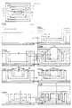
- FIG. 1a shows the cell construction
- FIG. 1b shows the cell layout
- FIG. 1c the cross section
- FIG. 2a shows the cell construction
- FIG. 2b shows the cell layout
- FIG. 2c the cross section
- FIG. 1 The production of an STC-on-bitline memory cell arrangement (FIGS. 2.4) will be explained in more detail below.
- FIG. 1 The production of a bitline-on-STC memory cell arrangement according to the invention (FIG. 1) is analogous with regard to the STC complex (FIG. 3) and is therefore not described further here.
- CMOS wells are formed in a p-doped silicon substrate with a LOGOS process field isolation areas and active areas and then LDD-MOS transistors, consisting of insulated polysilicon word lines 12 with silicon dioxide cover insulation, lateral insulation spacers and source 7 and drain regions 9.
- n-type polysilicon layer is formed as the bottom floor plate layer 2a, which forms the drain region 9 a conductive stamp 14 contacted, deposited.
- a 1 ⁇ m thick planarized auxiliary insulator layer 17 is applied (FIG. 4e; FIG. 3b) and a steep-sided breakthrough with a width of 1 is applied via a resist mask with an anisotropic selective RIE process, which is stopped on the bottom base plate layer 2A , 6 ⁇ m are introduced into the auxiliary insulator layer 17.
- an n-type polysilicon layer with a thickness of 175 nm is deposited as the first conductive lamella layer, then a first thin auxiliary insulation layer 18 with a thickness of 180 nm is applied (FIG.
- the layer stack of all lamella layers lying on the surface of the thick auxiliary insulation layer 17 is subsequently removed using an RIE process, the surfaces of the thick auxiliary insulation layer 17 and the thin auxiliary insulation layers 18 remaining in the steep-sided opening being exposed and the upper ends of the layers being arranged vertically in the opening Polysilicon lamellae 3 are separated from one another (FIG. 3f).
- the polysilicon lamellae 3 which are vertically free in the area of the previous steep-sided opening, are removed vertically by the anisotropic RIE method by the thickness of the lowest base plate layer 2A, the RIE -Procedure is stopped on the upper insulation layer 13.
- the self-adjusting etching of the bottom floor slab layer 2A takes place in the area outside the previous steep-sided opening and thus the separation of the storage electrodes 1 of adjacent storage cells, the conductive floor slab 2 connecting the conductive lamellae horizontally, that of the bottom floor slab layer 2A and horizontal parts of the polysilicon lamella layers is thinned by the thickness of the lowermost base plate layer, but is not cut through (FIG. 3h).
- an ONO storage dielectric 4 with a silicon dioxide equivalent thickness of 3 nm is produced from a 3 nm thick silicon dioxide layer, a 10 nm thick LPCVD silicon nitride layer and a reoxidation of the silicon nitride layer.
- n-doped polysilicon layer is then deposited and structured as a cell plate 5 with a thickness of 150 nm, which completely fills the spaces between the polysilicon fins 3.
- planarizing cover insulation layer 19 is deposited and structured (FIG. 3i; FIG. 4f).
Landscapes
- Engineering & Computer Science (AREA)
- Physics & Mathematics (AREA)
- Condensed Matter Physics & Semiconductors (AREA)
- General Physics & Mathematics (AREA)
- Computer Hardware Design (AREA)
- Microelectronics & Electronic Packaging (AREA)
- Power Engineering (AREA)
- Manufacturing & Machinery (AREA)
- Semiconductor Memories (AREA)
- Dram (AREA)
Claims (5)
- Dispositif de cellules de mémoire à transistor unique pour une mémoire semiconductrice dynamique à intégration maximale, composé d'une zone à isolation de champ et d'une zone active d'un substrat semiconducteur monocristallin, dans lequel sont intégrés un transistor sélecteur à effet de champ à sélection MOS avec une ligne de mots (12), une région de source (7) et une région de drain (9), d'une ligne de bits (6) contactée par la région de source (7) et d'une électrode de stockage (1) d'un condensateur de mémoire à capacité empilée, contactée par la région de drain (9), dont l'électrode chapeau (5) est conçue sous forme de plaque de cellule de toutes les cellules de mémoire d'un bloc de matrice de mémoire, le dispositif de cellules de mémoire étant sélectionné de sorte
que l'électrode de stockage (1) se compose d'un agencement concentrique de lamelles (3) conductrices à fermeture annulaire, orienté verticalement par rapport à la surface du substrat semiconducteur monocristallin, dont l'épaisseur de paroi et la distance mutuelle sont équidistantes et de taille à peu prés égale,
que la lamelle la plus interne (3B) remplit entièrement le centre de l'électrode de stockage (1),
que chacune des lamelles (3) passe dans une couche de plaques de fond (2), en direction du substrat semiconducteur, chacune des lamelles annulaires (3) étant ainsi fermée vers le bas et formant, avec sa couche de plaques de fond (2), un élément en forme de godet,
que chacune de ces couches de plaques de fond (2) contacte sur l'ensemble de la surface renfermée par la lamelle correspondante (3) la couche de plaques de fond plus grande sous-jacente (2) de la lamelle adjacente plus grande (3),
que la couche de plaques de fond située la plus en bas (2), dont la surface est déterminée par l'étendue de la lamelle la plus externe (3A), contacte une couche de base de plaques de fond de même taille (2A), établissant le contact avec la région de drain (9) du transistor sélecteur MOS (2A), l'épaisseur de cette couche étant inférieure à celle d'une couche de plaques de fond (2),
que l'électrode de stockage (1) est recouverte d'une fine couche conforme de diélectrique de stockage (4) et d'une couche de plaques de cellules (5), les espaces restants entre les lamelles (3) et l'électrode de stockage (1) de chaque cellule de mémoire étant ainsi remplis entièrement par la couche de plaques de cellules (5) et les flancs extérieurs de l'électrode de stockage (1) ainsi que les espaces entre les électrodes de stockage (1) de cellules de mémoire voisines étant également recouverts de la plaque de cellule (5), à l'exception de percées dues à la conception. - Dispositif de cellules de mémoire à transistor unique selon la revendication 1, caractérisé en ce que les lamelles (3) se terminent à un niveau uniforme, au-dessus du niveau de la surface du substrat semiconducteur, indépendamment du relief de leurs couches de plaques de fond (2) et indépendamment du relief des éléments de cellules de mémoire agencées au-dessous.
- Dispositif de cellules de mémoire à transistor unique selon l'une quelconque des revendications précédentes, caractérisé
en ce qu'une ligne de bits (6) est agencée de façon isolée sur le condensateur de mémoire à capacité empilée, la partie (21) de la ligne de bits (6) agencée dans l'ouverture de contact de source (8) étant configurée sous forme d'empreinte et étant aplanie par rapport au niveau de la ligne de bits, I'établissement du contact entre le drain et l'électrode de stockage (1) se faisant par l'intermédiaire d'un contact direct entre la couche de base des plaques de fond (2a) et la région de drain (9). - Procédé de production d'un dispositif de cellules de mémoire à transistor unique selon les revendications 1 et 2, caractérisé
en ce qu'après la production du transistor sélecteur à effet de champ MOS, avec une ligne de mots isolée de tous les côtés (12) et des régions de source (7) et de drain (9), et après la séparation d'un isolateur de plan intermédiaire et l'établissement d'une ouverture de contact de drain (10), une mince couche de base de plaques de fond (2a) ainsi qu'une couche isolante auxiliaire épaisse (17), dont l'épaisseur définit la dimension verticale de l'électrode de stockage (1), sont aplanies et séparées,
en ce qu'une percée à flanc raide est ensuite pratiquée dans cette dernière, jusqu'à la couche de base des plaques de fond (2a), par l'intermédiaire d'une gravure au plasma sélective anisotrope, I'étendue de cette percée déterminant la dimension externe de l'électrode de stockage (1),
en ce que, en commençant par la séparation d'une première couche de lamelles conductrices (3A) on sépare ensuite alternativement une couche de lamelles (3), d'une épaisseur supérieure à l'épaisseur de la couche de base des plaques de fond (2A), et une couche isolante sacrificielle (18), d'une épaisseur comparable à l'épaisseur d'une couche de lamelles (3), un processus de gravure en retrait plasma-chimique anisotrope étant effectué au moins après la séparation de la couche isolante sacrificielle (18), ce processus s'arrêtant sélectivement au niveau de la couche de lamelles (3) séparée en dernier lieu, les régions de couche horizontales de la couche isolante sacrificielle (18) étant ainsi entièrement éliminées, la couche isolante sacrificielle (18) étant toutefois maintenue sur la paroi verticale de la percée à flanc raide, de sorte à y former après plusieurs répétitions desdits procédés de séparation de couche et de gravure en retrait, une structure de lamelles verticale composée de lamelles conductrices (3) et de couches isolantes sacrificielles (18) agencées entre celles-ci,
en ce qu'après la séparation de la dernière des couches de lamelles conductrices (3B), fermant complètement la percée à flanc raide dans la couche isolante auxiliaire épaisse (17), on réalise une étape de gravure au plasma anisotrope, éliminant la pile stratifiée de toutes les couches de lamelles conductrices (3) agencées sur la surface de la couche isolante auxiliaire épaisse, de façon sélective par rapport aux couches isolantes (17, 18), les extrémités supérieures des lamelles verticales (3) agencées au niveau de la percée à flanc raide étant ainsi dégagées et séparées les unes des autres,
en ce que les couches isolantes sacrificielles (18) enrobées entre les lamelles verticales (3), ainsi que la couche isolante épaisse (17) sont ensuite éliminées complètement au moyen d'un procédé de gravure isotrope sélective par rapport aux couches de lamelles (3) et de plaques de fond (2),
en ce que la couche de base des plaques de fond (2A) est ensuite éliminée en-dehors de l'électrode de stockage (1) par une gravure au plasma anisotrope, lors de laquelle l'électrode de stockage (1) sert de masque de gravure à auto-ajustement, réalisant ainsi la séparation électrique des électrodes de stockage (1) de toutes les cellules de mémoire, les dimensions verticales de l'électrode de stockage (1) étant simultanément réduites de la valeur de l'épaisseur de la couche de base des plaques de fond (2A),
en ce que les surfaces dégagées de l'électrode de stockage (1) sont ensuite nettoyées et lissées au cours d'étapes de gravure et de nettoyage,
en ce qu'une diélectrique de stockage fine, à couverture régulière (4), est agencée ensuite sur la surface tridimensionnelle de l'électrode de stockage (1) par des procédés d'oxydation et de séparation,
en ce qu'une couche conductrice, remplissant entièrement les espaces restants entre les lamelles (3) de l'électrode de stockage (1) et formant une plaque de cellule (5) est alors séparée,
en ce qu'une couche isolante de couverture d'aplanissement (19) est ensuite formée par un procédé de séparation, et
en ce que la cellule de mémoire est alors complétée au cours des étapes ultérieures du processus. - Procédé selon la revendication 4, caractérisé en ce qu'une couche isolante inférieure (11) est séparée après la production de la ligne de mots isolée de tous les côtés (12) et des régions de source (7) et de drain (9),
en ce que des ouvertures de contact de drain (10) sont ensuite appliquées dans celle-ci par l'intermédiaire d'un masque de vernis au cours d'un procédé de gravure au plasma,
en ce que le condensateur de mémoire à capacité empilée est alors produit, en commençant par la séparation de la couche de base des plaques de fond (2a), contactant la région de drain (9), jusqu'à la séparation d'une couche isolante de couverture d'aplanissement (19),
en ce qu'une ouverture de contact de la ligne de bits (8) est ensuite pratiquée dans celle-ci au-dessus de la région de source (7) au cours d'une étape de gravure au plasma anisotrope, le procédé de gravure étant arrêté sélectivement sur la couche des plaques de cellule (5),
en ce que la couche des plaques de cellule (5) est alors gravée dans l'ouverture de contact de la ligne de bits (8) au cours d'une étape ultérieure de gravure au plasma, la diélectrique de stockage (4) arrêtant le procédé,
en ce que les flancs dégagés de la couche des plaques de cellule (5) dans l'ouverture de contact de la ligne de bits (8) sont gravés en retrait derrière les flancs de la couche isolante de couverture (19) de l'ouverture de contact de la ligne de bits (8), au cours d'un procédé de gravure isotrope sélective,
en ce qu'une mince couche isolante d'espacement (20) est ensuite séparée de façon isotrope,
en ce que celle-ci est alors de nouveau éliminée sur la surface horizontale de la couche isolante de couverture (19) et sur la surface de base de l'ouverture de contact de la ligne de bits (8) au cours d'une étape de gravure au plasma anisotrope sans masque,
en ce que cette étape de gravure au plasma anisotrope ouvre en outre complètement l'ouverture de contact de la ligne de bits (8) jusqu'à la surface de la région de source (7) du substrat semiconducteur monocristallin, la mince couche isolante (20) étant maintenue sur les flancs gravés en retrait de la couche de plaques de cellule (5) de l'ouverture de contact de la ligne de bits (8),
en ce qu'une couche conductrice est ensuite séparée de façon isotrope, celle-ci remplissant entièrement l'ouverture de contact de la ligne de bits (8),
en ce que la couche conductrice est alors gravée en retrait par un procédé de gravure au plasma d'aplanissement, à peu près jusqu'au niveau de la surface de la couche isolante de couverture d'aplanissement (19), de sorte que la couche conductrice est maintenue dans l'ouverture de contact de la ligne de bits (8) sous forme d'une empreinte conductrice aplanie (21)
en ce que la ligne de bits (6), contactant l'empreinte conductrice (21) de l'ouverture de la ligne de bits (8) est ensuite formée, et
en ce que la préparation de la cellule de mémoire est alors achevée de façon conventionnelle.
Priority Applications (1)
| Application Number | Priority Date | Filing Date | Title |
|---|---|---|---|
| EP94101691A EP0600850B1 (fr) | 1990-02-23 | 1991-02-14 | Structure de cellule DRAM avec condensateur sur la ligne de bit et procédé de sa manufacture |
Applications Claiming Priority (2)
| Application Number | Priority Date | Filing Date | Title |
|---|---|---|---|
| DD338097 | 1990-02-23 | ||
| DD338097A DD299990A5 (de) | 1990-02-23 | 1990-02-23 | Ein-Transistor-Speicherzellenanordnung und Verfahren zu deren Herstellung |
Related Child Applications (2)
| Application Number | Title | Priority Date | Filing Date |
|---|---|---|---|
| EP94101691A Division EP0600850B1 (fr) | 1990-02-23 | 1991-02-14 | Structure de cellule DRAM avec condensateur sur la ligne de bit et procédé de sa manufacture |
| EP94101691.7 Division-Into | 1994-02-04 |
Publications (3)
| Publication Number | Publication Date |
|---|---|
| EP0443439A2 EP0443439A2 (fr) | 1991-08-28 |
| EP0443439A3 EP0443439A3 (en) | 1991-10-02 |
| EP0443439B1 true EP0443439B1 (fr) | 1995-10-18 |
Family
ID=5616632
Family Applications (2)
| Application Number | Title | Priority Date | Filing Date |
|---|---|---|---|
| EP91102082A Expired - Lifetime EP0443439B1 (fr) | 1990-02-23 | 1991-02-14 | Dispositif de mémoire comprenant un transistor et son procédé de fabrication |
| EP94101691A Expired - Lifetime EP0600850B1 (fr) | 1990-02-23 | 1991-02-14 | Structure de cellule DRAM avec condensateur sur la ligne de bit et procédé de sa manufacture |
Family Applications After (1)
| Application Number | Title | Priority Date | Filing Date |
|---|---|---|---|
| EP94101691A Expired - Lifetime EP0600850B1 (fr) | 1990-02-23 | 1991-02-14 | Structure de cellule DRAM avec condensateur sur la ligne de bit et procédé de sa manufacture |
Country Status (4)
| Country | Link |
|---|---|
| EP (2) | EP0443439B1 (fr) |
| AT (1) | ATE129363T1 (fr) |
| DD (1) | DD299990A5 (fr) |
| DE (3) | DE59106693D1 (fr) |
Families Citing this family (13)
| Publication number | Priority date | Publication date | Assignee | Title |
|---|---|---|---|---|
| KR930009594B1 (ko) * | 1991-01-30 | 1993-10-07 | 삼성전자 주식회사 | 고집적 반도체 메모리장치 및 그 제조방법 |
| GB2279176B (en) * | 1991-05-23 | 1995-06-07 | Samsung Electronics Co Ltd | DRAM cell capacitor |
| KR940006587B1 (ko) * | 1991-05-23 | 1994-07-22 | 삼성전자 주식회사 | 디램셀의 캐패시터 제조방법 |
| TW243541B (fr) * | 1991-08-31 | 1995-03-21 | Samsung Electronics Co Ltd | |
| GB2293690B (en) * | 1991-08-31 | 1996-06-19 | Samsung Electronics Co Ltd | Manufacturing method for a semiconductor device |
| TW222710B (fr) * | 1991-09-07 | 1994-04-21 | Samsung Electronics Co Ltd | |
| US5150276A (en) * | 1992-01-24 | 1992-09-22 | Micron Technology, Inc. | Method of fabricating a vertical parallel cell capacitor having a storage node capacitor plate comprising a center fin effecting electrical communication between itself and parallel annular rings |
| DE4221434A1 (de) * | 1992-06-30 | 1994-01-05 | Siemens Ag | Herstellverfahren für einen Speicherkondensator |
| DE4222467C1 (fr) * | 1992-07-08 | 1993-06-24 | Siemens Ag, 8000 Muenchen, De | |
| JP2953220B2 (ja) * | 1992-10-30 | 1999-09-27 | 日本電気株式会社 | 半導体装置の製造方法 |
| KR950021644A (ko) * | 1993-12-31 | 1995-07-26 | 김주용 | 반도체 기억장치 및 그 제조방법 |
| KR0126640B1 (ko) * | 1994-05-07 | 1998-04-02 | 김주용 | 반도체소자 및 그 제조방법 |
| GB2322964B (en) * | 1997-03-07 | 2001-10-17 | United Microelectronics Corp | Polysilicon CMP process for high-density DRAM cell structures |
Family Cites Families (10)
| Publication number | Priority date | Publication date | Assignee | Title |
|---|---|---|---|---|
| US4855801A (en) * | 1986-08-22 | 1989-08-08 | Siemens Aktiengesellschaft | Transistor varactor for dynamics semiconductor storage means |
| JP2702121B2 (ja) * | 1987-02-25 | 1998-01-21 | 日本電気株式会社 | 半導体記憶装置 |
| JPS6474752A (en) * | 1987-09-17 | 1989-03-20 | Matsushita Electric Ind Co Ltd | Manufacture of semiconductor device |
| US4872050A (en) * | 1988-03-15 | 1989-10-03 | Mitsubishi Denki Kabushiki Kaisha | Interconnection structure in semiconductor device and manufacturing method of the same |
| JP2755591B2 (ja) * | 1988-03-25 | 1998-05-20 | 株式会社東芝 | 半導体記憶装置 |
| JPH01302851A (ja) * | 1988-05-31 | 1989-12-06 | Fujitsu Ltd | 半導体メモリのメモリセル構造 |
| JPH01302852A (ja) * | 1988-05-31 | 1989-12-06 | Fujitsu Ltd | 半導体メモリのメモリセル構造 |
| JPH01308069A (ja) * | 1988-06-07 | 1989-12-12 | Fujitsu Ltd | 半導体メモリのメモリセル構造 |
| DE3918924C2 (de) * | 1988-06-10 | 1996-03-21 | Mitsubishi Electric Corp | Herstellungsverfahren für eine Halbleiterspeichereinrichtung |
| JP2724209B2 (ja) * | 1989-06-20 | 1998-03-09 | シャープ株式会社 | 半導体メモリ素子の製造方法 |
-
1990
- 1990-02-23 DD DD338097A patent/DD299990A5/de unknown
-
1991
- 1991-02-14 AT AT91102082T patent/ATE129363T1/de not_active IP Right Cessation
- 1991-02-14 DE DE59106693T patent/DE59106693D1/de not_active Expired - Fee Related
- 1991-02-14 EP EP91102082A patent/EP0443439B1/fr not_active Expired - Lifetime
- 1991-02-14 DE DE59109236T patent/DE59109236D1/de not_active Expired - Fee Related
- 1991-02-14 EP EP94101691A patent/EP0600850B1/fr not_active Expired - Lifetime
- 1991-02-19 DE DE4105501A patent/DE4105501A1/de not_active Withdrawn
Non-Patent Citations (2)
| Title |
|---|
| IEEE TRANSACTIONS ON ELECTRON DEVICES, Band 35, Nr. 10, Teilen 1/2, Oktober 1988, Seiten 1591-1595, New York, US; S.-I. KIMURA et al.: "An optically delineated 4.2-mum2 self-aligned isolated-plate stacked-capacitor DRAM cell" * |
| PATENT ABSTRACTS OF JAPAN, Band 13, Nr. 295 (E-783)(3643), 7. Juli 1989 ; & JP-A-1 074 752 * |
Also Published As
| Publication number | Publication date |
|---|---|
| EP0443439A2 (fr) | 1991-08-28 |
| EP0600850A1 (fr) | 1994-06-08 |
| DD299990A5 (de) | 1992-05-14 |
| DE59106693D1 (de) | 1995-11-23 |
| EP0443439A3 (en) | 1991-10-02 |
| DE4105501A1 (de) | 1991-08-29 |
| DE59109236D1 (de) | 2002-07-04 |
| EP0600850B1 (fr) | 2002-05-29 |
| ATE129363T1 (de) | 1995-11-15 |
Similar Documents
| Publication | Publication Date | Title |
|---|---|---|
| EP0744772B1 (fr) | Cellule de stockage DRAM à transistor vertical et son procédé de fabrication | |
| EP0744771B1 (fr) | Procédé de fabrication d'une cellule de stockage DRAM avec transistor vertical | |
| DE4031411C2 (de) | Verfahren zur Herstellung einer einen Kondensator aufweisenden Halbleitervorrichtung | |
| DE19941148B4 (de) | Speicher mit Grabenkondensator und Auswahltransistor und Verfahren zu seiner Herstellung | |
| DE19843979C1 (de) | Speicherzellenanordnung mit ferroelektrischem oder dynamischen Speicherzellen und entsprechendes Herstellungsverfahren | |
| DE69733055T2 (de) | Herstellungsverfahren für DRAM-Stapelkondensator | |
| EP0875937A2 (fr) | Réseau de cellules DRAM et son procédé de fabrication | |
| EP0443439B1 (fr) | Dispositif de mémoire comprenant un transistor et son procédé de fabrication | |
| DE102004043858A1 (de) | Verfahren zur Herstellung einer Speicherzelle, einer Speicherzellenanordnung und Speicherzellenanordnung | |
| DE4213945A1 (de) | Speicherkondensator und verfahren zu dessen herstellung | |
| EP0936673B1 (fr) | Réseau de cellules de mémoire et procédé de fabrication | |
| DE19842704C2 (de) | Herstellverfahren für einen Kondensator mit einem Hoch-epsilon-Dielektrikum oder einem Ferroelektrikum nach dem Fin-Stack-Prinzip unter Einsatz einer Negativform | |
| DE19546999C1 (de) | Verfahren zur Herstellung von Kondensatoren in einer Halbleiteranordnung | |
| EP0945901A1 (fr) | Réseau de cellules DRAM à transistor vertical et son procédé de fabrication | |
| DE19929859B4 (de) | Herstellungsverfahren für Trenchkondensator | |
| DE10308888A1 (de) | Anordnung von Kondensatoren zur Erhöhung der Speicherkapazität in einem Halbleitersubstrat | |
| EP1125328B1 (fr) | Procede de production d'un ensemble de cellules de memoire ram dynamique | |
| WO2000019529A1 (fr) | Ensemble circuit integre comportant des transistors verticaux, et son procede de production | |
| WO1997044826A1 (fr) | Dispositif a cellules dram et son procede de fabrication | |
| DE19832095C1 (de) | Stapelkondensator-Herstellungsverfahren | |
| EP1129482B1 (fr) | Procédé de production d'une configuration de cellules DRAM | |
| DE4406850C1 (de) | Verfahren zur Herstellung einer Halbleiterstruktur, wenigstens bestehend aus einem Transistor und einer Kondensatorelektrode | |
| WO1998011604A1 (fr) | Procede de production d'une matrice cellulaire a dram | |
| DE4409718A1 (de) | Kondensator für ein Halbleiterbauelement und Verfahren zu seiner Herstellung | |
| DE19923262C1 (de) | Verfahren zur Erzeugung einer Speicherzellenanordnung |
Legal Events
| Date | Code | Title | Description |
|---|---|---|---|
| PUAI | Public reference made under article 153(3) epc to a published international application that has entered the european phase |
Free format text: ORIGINAL CODE: 0009012 |
|
| PUAL | Search report despatched |
Free format text: ORIGINAL CODE: 0009013 |
|
| AK | Designated contracting states |
Kind code of ref document: A2 Designated state(s): AT CH DE FR GB IT LI NL |
|
| AK | Designated contracting states |
Kind code of ref document: A3 Designated state(s): AT CH DE FR GB IT LI NL |
|
| 17P | Request for examination filed |
Effective date: 19911017 |
|
| RAP1 | Party data changed (applicant data changed or rights of an application transferred) |
Owner name: INSTITUT FUER HALBLEITERPHYSIK FRANKFURT (ODER) GM |
|
| 17Q | First examination report despatched |
Effective date: 19930827 |
|
| GRAA | (expected) grant |
Free format text: ORIGINAL CODE: 0009210 |
|
| AK | Designated contracting states |
Kind code of ref document: B1 Designated state(s): AT CH DE FR GB IT LI NL |
|
| PG25 | Lapsed in a contracting state [announced via postgrant information from national office to epo] |
Ref country code: IT Free format text: LAPSE BECAUSE OF FAILURE TO SUBMIT A TRANSLATION OF THE DESCRIPTION OR TO PAY THE FEE WITHIN THE PRE;WARNING: LAPSES OF ITALIAN PATENTS WITH EFFECTIVE DATE BEFORE 2007 MAY HAVE OCCURRED AT ANY TIME BEFORE 2007. THE CORRECT EFFECTIVE DATE MAY BE DIFFERENT FROM THE ONE RECORDED.SCRIBED TIME-LIMIT Effective date: 19951018 Ref country code: NL Free format text: LAPSE BECAUSE OF FAILURE TO SUBMIT A TRANSLATION OF THE DESCRIPTION OR TO PAY THE FEE WITHIN THE PRESCRIBED TIME-LIMIT Effective date: 19951018 |
|
| REF | Corresponds to: |
Ref document number: 129363 Country of ref document: AT Date of ref document: 19951115 Kind code of ref document: T |
|
| XX | Miscellaneous (additional remarks) |
Free format text: TEILANMELDUNG 94101691.7 EINGEREICHT AM 14/02/91. |
|
| REF | Corresponds to: |
Ref document number: 59106693 Country of ref document: DE Date of ref document: 19951123 |
|
| PG25 | Lapsed in a contracting state [announced via postgrant information from national office to epo] |
Ref country code: GB Effective date: 19960214 |
|
| REG | Reference to a national code |
Ref country code: CH Ref legal event code: NV Representative=s name: A. BRAUN, BRAUN, HERITIER, ESCHMANN AG PATENTANWAE |
|
| ET | Fr: translation filed | ||
| NLV1 | Nl: lapsed or annulled due to failure to fulfill the requirements of art. 29p and 29m of the patents act | ||
| GBV | Gb: ep patent (uk) treated as always having been void in accordance with gb section 77(7)/1977 [no translation filed] |
Effective date: 19951213 |
|
| GBT | Gb: translation of ep patent filed (gb section 77(6)(a)/1977) |
Effective date: 19960524 |
|
| PLBE | No opposition filed within time limit |
Free format text: ORIGINAL CODE: 0009261 |
|
| STAA | Information on the status of an ep patent application or granted ep patent |
Free format text: STATUS: NO OPPOSITION FILED WITHIN TIME LIMIT |
|
| GBPC | Gb: european patent ceased through non-payment of renewal fee |
Effective date: 19960214 |
|
| 26N | No opposition filed | ||
| REG | Reference to a national code |
Ref country code: CH Ref legal event code: PUE Owner name: INSTITUT FUER HALBLEITERPHYSIK FRANKFURT (ODER) GM Ref country code: CH Ref legal event code: NV Representative=s name: SIEMENS SCHWEIZ AG |
|
| REG | Reference to a national code |
Ref country code: FR Ref legal event code: TP |
|
| PGFP | Annual fee paid to national office [announced via postgrant information from national office to epo] |
Ref country code: CH Payment date: 20010511 Year of fee payment: 11 |
|
| PGFP | Annual fee paid to national office [announced via postgrant information from national office to epo] |
Ref country code: AT Payment date: 20020123 Year of fee payment: 12 |
|
| PG25 | Lapsed in a contracting state [announced via postgrant information from national office to epo] |
Ref country code: CH Free format text: LAPSE BECAUSE OF NON-PAYMENT OF DUE FEES Effective date: 20020228 Ref country code: LI Free format text: LAPSE BECAUSE OF NON-PAYMENT OF DUE FEES Effective date: 20020228 |
|
| REG | Reference to a national code |
Ref country code: CH Ref legal event code: PL |
|
| PG25 | Lapsed in a contracting state [announced via postgrant information from national office to epo] |
Ref country code: AT Free format text: LAPSE BECAUSE OF NON-PAYMENT OF DUE FEES Effective date: 20030214 |
|
| PGFP | Annual fee paid to national office [announced via postgrant information from national office to epo] |
Ref country code: DE Payment date: 20050421 Year of fee payment: 15 |
|
| PGFP | Annual fee paid to national office [announced via postgrant information from national office to epo] |
Ref country code: FR Payment date: 20060216 Year of fee payment: 16 |
|
| PG25 | Lapsed in a contracting state [announced via postgrant information from national office to epo] |
Ref country code: DE Free format text: LAPSE BECAUSE OF NON-PAYMENT OF DUE FEES Effective date: 20060901 |
|
| REG | Reference to a national code |
Ref country code: FR Ref legal event code: ST Effective date: 20071030 |
|
| PG25 | Lapsed in a contracting state [announced via postgrant information from national office to epo] |
Ref country code: FR Free format text: LAPSE BECAUSE OF NON-PAYMENT OF DUE FEES Effective date: 20070228 |