EP0443439A2 - Dispositif de mémoire comprenant un transistor et son procédé de fabrication - Google Patents
Dispositif de mémoire comprenant un transistor et son procédé de fabrication Download PDFInfo
- Publication number
- EP0443439A2 EP0443439A2 EP91102082A EP91102082A EP0443439A2 EP 0443439 A2 EP0443439 A2 EP 0443439A2 EP 91102082 A EP91102082 A EP 91102082A EP 91102082 A EP91102082 A EP 91102082A EP 0443439 A2 EP0443439 A2 EP 0443439A2
- Authority
- EP
- European Patent Office
- Prior art keywords
- layer
- insulation layer
- conductive
- contact window
- bit line
- Prior art date
- Legal status (The legal status is an assumption and is not a legal conclusion. Google has not performed a legal analysis and makes no representation as to the accuracy of the status listed.)
- Granted
Links
Images


Classifications
-
- H—ELECTRICITY
- H01—ELECTRIC ELEMENTS
- H01L—SEMICONDUCTOR DEVICES NOT COVERED BY CLASS H10
- H01L23/00—Details of semiconductor or other solid state devices
- H01L23/52—Arrangements for conducting electric current within the device in operation from one component to another, i.e. interconnections, e.g. wires, lead frames
- H01L23/522—Arrangements for conducting electric current within the device in operation from one component to another, i.e. interconnections, e.g. wires, lead frames including external interconnections consisting of a multilayer structure of conductive and insulating layers inseparably formed on the semiconductor body
- H01L23/5226—Via connections in a multilevel interconnection structure
-
- H—ELECTRICITY
- H10—SEMICONDUCTOR DEVICES; ELECTRIC SOLID-STATE DEVICES NOT OTHERWISE PROVIDED FOR
- H10B—ELECTRONIC MEMORY DEVICES
- H10B12/00—Dynamic random access memory [DRAM] devices
- H10B12/01—Manufacture or treatment
- H10B12/02—Manufacture or treatment for one transistor one-capacitor [1T-1C] memory cells
- H10B12/03—Making the capacitor or connections thereto
- H10B12/033—Making the capacitor or connections thereto the capacitor extending over the transistor
-
- H—ELECTRICITY
- H10—SEMICONDUCTOR DEVICES; ELECTRIC SOLID-STATE DEVICES NOT OTHERWISE PROVIDED FOR
- H10B—ELECTRONIC MEMORY DEVICES
- H10B12/00—Dynamic random access memory [DRAM] devices
- H10B12/30—DRAM devices comprising one-transistor - one-capacitor [1T-1C] memory cells
- H10B12/31—DRAM devices comprising one-transistor - one-capacitor [1T-1C] memory cells having a storage electrode stacked over the transistor
- H10B12/318—DRAM devices comprising one-transistor - one-capacitor [1T-1C] memory cells having a storage electrode stacked over the transistor the storage electrode having multiple segments
-
- H—ELECTRICITY
- H01—ELECTRIC ELEMENTS
- H01L—SEMICONDUCTOR DEVICES NOT COVERED BY CLASS H10
- H01L2924/00—Indexing scheme for arrangements or methods for connecting or disconnecting semiconductor or solid-state bodies as covered by H01L24/00
- H01L2924/0001—Technical content checked by a classifier
- H01L2924/0002—Not covered by any one of groups H01L24/00, H01L24/00 and H01L2224/00
Definitions
- the invention relates to a one-transistor memory cell arrangement and a method for its production, in particular for highly integrated dynamic semiconductor memories.
- the basic structure for dynamic semiconductor memories based on the principle of the one-transistor cell consists of a MOS selection transistor and a storage capacitor with a storage capacity of 30 to 50 fF, which contains the logical information as a stored charge.
- the selection transistor can be controlled via a word line. Its drain region is connected to an electrode of the storage capacitor, while its source region is connected to the outside via a bit line with source regions of further memory cells lying in the bit line direction.
- the storage capacitors are generally formed as a planar arrangement by a highly doped substrate surface section, an overlying storage dielectric (usually silicon dioxide) and a polysilicon cell plate.
- STC trench or stack capacitor
- the STC cell concept is distinguished from the trench cell concept by the fact that the storage capacity is largely electrically decoupled from the active silicon. As a result, the active silicon generally remains morphologically undisturbed except for the contacting of a lower storage electrode.
- the substrate defects typical of the trench cell concepts or the technological measures generally required to eliminate these defects and the lateral interaction of adjacent storage capacities via the silicon substrate avoided in principle and guaranteed a natural, high ALPHA immunity without special measures.
- the storage capacitor consists of two stacked doped polysilicon layers with a storage dielectric in between.
- the lower polysilicon layer acts as a storage electrode and is connected to the drain region of the selection transistor.
- the upper polysilicon layer acts as a common cell plate of a memory matrix.
- the electrode stack overlaps the gate of the selection transistor (cf. Koyanagi, IEDM Tech. Dig. 1978, pp. 348-351).
- EP-PS 0191612 An improved STC variant is known from EP-PS 0191612, in which the cell plate overlaps the edge of the storage electrode, as a result of which its side flank is obtained as an area contribution for a higher storage capacity.
- the simultaneous filling of the bit line contact window with the production of the storage electrode also solves the problem of the bit line break on the flanks of the bit line contact window.
- EP-PS 0263941 these advantages can be increased by increasing the thickness of the storage electrode.
- EP-PS 0223616 a method in which a trench is produced by deepening the drain contact window into the silicon substrate by means of an RIE process, the topology of which also contributes to an increase in the capacitive area after the storage electrode layer has been deposited.
- An even larger storage capacity can be achieved by combining the relief contributions of a thick storage electrode and a trench in the drain contact window (IEDM Tech. Dig., 1988, pp. 600-603).
- the three-dimensional SIC variants listed produce a topological relief which makes it difficult to break off bit line contact when the bit line is passed over the storage capacitor.
- IEDM Tech. Dig. 1988, S. 596-599 a solution is known in which the bit line is carried out under the storage capacity.
- the bit line is produced after the selection transistor has been completed in such a way that the bit line is guided laterally past the later drain contact window for the storage electrode. This opens up the basic possibility of vertically enlarging the STG complex without problems with bit line structuring and contacting.
- an STC cell concept (“fin type”) is known from EP-PS 0295709, in which the storage electrode consists of a mutually contacted multiple polysilicon stack which overlaps the selection transistor. These polysilicon fins are enclosed on all sides by the storage dielectric and a common polysilicon cell plate.
- Ema u. a. describe in IEDM Tech. Dig. 1988, p.592-595 both possibilities of the bit line routing below and above a storage capacity of the "fin type".
- bit line For memories greater than or equal to 16 MdRAM, the bit line must be arranged under the STC complex. Such complexly structured storage electrodes are difficult to control in terms of production technology (cf. IEDM Tech. Dig. 1989, pp. 31-34). Inoue et al. a. ibid with an SSC cell concept for 64 MdRAM or 256 MdRAM, a solution in which the bit line is arranged under the STC complex and storage electrodes of the "fin type" overlap each other into neighboring cell areas.
- a disadvantage of the latter two solutions irrespective of whether the polysilicon fins forming the storage electrode stack overlap only the own cell area or also the neighboring cell areas, is that during processing a processing phase occurs in which the horizontally arranged polysilicon fins are exposed to several process steps in a cantilever manner are. These process steps, such as wet etching and cleaning steps, oxidation, insulator and polysilicon CVD deposition, represent significant mechanical, chemical, and thermal stresses for these sensitive, cantilevered storage electrode configurations.
- the fins are preferably very thin (less than or equal to 100 nm) with a large length to thickness ratio and only in line with the other fins of the same storage electrode or grown on the single-crystalline silicon substrate.
- the stability of such self-supporting storage electrodes is low and, as a result, the yield in the production of the storage cell is adversely affected.
- a further disadvantage is that the long and narrow spaces between the polysilicon fins lie parallel to the silicon substrate surface and can only be reached, for example, by wet etching and cleaning processes via shaft-shaped channels lying perpendicular to it. This results in unfavorable transport, removal and exchange conditions for liquid and gaseous media in the micro areas of the storage electrode configuration, in particular for the surface treatment of the self-supporting polysilicon fins by wet etching and cleaning processes, but also for the subsequent CVD coating processes for the storage insulator and the polysilicon cell plate .
- the aim of the invention is a one-transistor memory cell arrangement for dynamic semiconductor memories and a method for their production, which significantly improve the quality and stability of the storage electrodes of the STC complex with high reproducibility, increase the yield of the production process and ensure an increase in the packing density.
- the object of the invention is to create a one-transistor memory cell arrangement for dynamic semiconductor memories and a method for their production, which are suitable for liquid and gaseous media when carrying out wet etching and cleaning processes and also coating methods, in particular when designing the STC Ensure complex, favorable conditions and avoid an adjustment-related safety distance when the STC complex is arranged above the bit line.
- the object is achieved by a one-transistor memory cell for highly integrated dynamic semiconductor memories, consisting of field isolation regions and active surface areas of a single-crystalline substrate, in which a MOS field effect transistor with an all-round insulated word line and a source and drain region is integrated, as well as one above arranged in the word line and largely covering the area of the memory cell stack capacitor (STC) complex, which is connected with its storage electrode to the drain area and its upper electrode as Cell plate of all memory cells of a memory matrix block is formed and a bit line contacted with the source region, solved in that the memory electrode consists of conductive lamellae arranged perpendicular to the substrate surface on a common, conductive base plate, each of which in the memory cell layout has a self-contained and closed band, the Width corresponds to the wall thickness of the slats, represents that each of the slats, starting with an outermost slat, which is arranged within the storage cell, encloses a smaller one, with
- the base plate in the memory cell layout corresponds exactly to the area enclosed by the periphery of the outermost lamella.
- the memory cell arrangement is designed in such a way that the base plate consists of a plurality of conductive layers, the layer thickness of a lowermost conductive base plate layer being less than or equal to the wall thickness of the slats, and the base plate surface corresponding at least to the area enclosed by the periphery of the outermost slat, that a second conductive layer is arranged on the lowermost conductive base plate layer, the layer thickness of which corresponds to the wall thickness of the outermost lamella and the area of which corresponds to the circumference of the outermost lamella enclosed area corresponds exactly to the fact that a third conductive layer is arranged on the second conductive layer, the layer thickness of which corresponds to the wall thickness of the next inner lamella and whose area corresponds exactly to the area enclosed by the circumference of the next inner lamella, and that further conductive layers
- the memory cell arrangement is characterized in that the lamellae end at a uniform height above the level of the substrate surface, regardless of the relief of the base plate with which they are contacted and regardless of the relief of the memory cell elements arranged under the base plate.
- a further embodiment of the memory cell arrangement is characterized in that a bit line is arranged on the insulated stack capacitor complex, the part of the bit line lying in the source contact window being stamp-like and planarized with respect to the top of the stack capacitor complex, and in that the drain contacting of the memory electrode by direct contact of the base plate with the Drain area in a drain contact window of a lower insulator layer, which is arranged on the isolated word lines and over the remaining memory cell regions with the exception of the contact windows of the source and drain regions.
- the memory cell arrangement is characterized in that the bit line covered with an upper insulation layer is arranged below the stack capacitor complex, the bit line being arranged on the lower insulation layer above the word line insulation and the lower insulation layer all regions of the memory cell, except the source and drain contact window area, covers that the bit line in the source contact window contacts the source area and that an insulated conductive Stamp that contacts the drain area in the drain contact window, penetrates the lower insulation layer, the bit line and the upper insulation layer and contacts the underside of the base plate.
- the vertical surface of the stamp is covered by an insulating jacket with a constant thickness in a self-adjusting manner.
- this memory cell arrangement is characterized in one embodiment in that the bit line is supplemented with a stamp diameter of approximately the bit line width at the point of penetration by a conductive ring which surrounds the insulated stamp with a constant thickness, the height of the conductive ring being at least that Corresponds to the thickness of the bit line and is electrically insulated from the drain region, the word line and the base plate.
- the object is further achieved by a method for producing a one-transistor memory cell arrangement in which n-type and p-type regions, field isolation regions and subsequently MOS field effect transistors with word lines and source and drain regions insulated on all sides in a single-crystal substrate conductive layer of a storage electrode, which produces the contact of a stacked capacitor to the drain region of the memory cell underneath, the stacked capacitor complex integrated in a memory matrix and the bit line contacted with the source region of the memory cell, and finally openings in the cell plate of the stacked capacitor complex are etched at contact points, that after the deposition of a lowermost conductive layer of the base plate, a thick auxiliary insulation layer is deposited in a planarized manner, that a steep-sided Durc Breakage is formed down to the lowest conductive layer, that subsequently begins and ends with a deposition of a conductive lamella layer alternately a conductive lamella layer and then a thin auxiliary insulation layer are deposited, the double sum of all conductive
- the method is characterized in that within the alternating sequence of the deposition of the conductive lamella layers and the thin auxiliary insulation layers, the thickness of the lamella layers corresponds at least to the thickness of the lowermost layer of the base plate and an anisotropic RIE etching process after the deposition of each thin auxiliary insulation layer is carried out, the layer stack lying on the surface of the thick auxiliary insulation layer is removed from all conductive lamella layers, whereby the upper ends of the lamellae perpendicular to the substrate surface are separated from each other, that after the isotropic removal of the thin auxiliary insulation layers between the lamellae and the remnants of the thick auxiliary insulation layer, the base plate the memory cell is structured in a mask-free, self-adjusting manner using an anisotropic RIE etching process.
- a further embodiment of the method according to the invention is characterized in that after the production of the word line which is insulated on all sides and the source and drain regions, a lower insulation layer is deposited, that drain contact windows are subsequently structured in the lower insulation layer, and that subsequently the stacked capacitor complex begins with the deposition of the lower one conductive layer of the bottom plate, which contacts the drain region, is formed that after the deposition of the planarized top insulation layer of the stacked capacitor complex, the bit line contact window is etched into this layer by means of an anisotropic RIE process, the cell plate stopping the process, which is then followed by an RIE process Bit line contact window is introduced into the cell plate, the storage dielectric stopping the process that subsequently the cell plate flanks in the Kon.
- the method according to the invention is characterized in that after the production of word lines which are insulated on all sides and the source and drain regions, a lower insulation layer is formed, that the source contact window is then structured, that the bit line is subsequently formed, the source contact being produced at the same time that an upper insulation layer covering the bit line is subsequently formed, and then a drain contact window is then etched through the upper insulation layer and the bit line in the lower insulation layer by an anisotropic etching process via a resist mask, the etching process being stopped before reaching the drain surface of the substrate and the parts of the field and word line insulation adjacent to the drain contact window are not damaged, that a further insulation layer is subsequently deposited isotropically, the thickness of this layer being clear is smaller than half the drain contact window width, that the drain contact window then follows up to the drain surface by means of an anisotropic RIE process of the substrate is deepened, whereby an all-round insulating self-adjusting covering of the drain contact window flanks and the perforated bit line is produced along
- the method is designed in such a way that in the anisotropic RIE process for etching the drain contact window, the lower insulation layer is initially only partially etched, that a conductive layer is then isotropically deposited, and then an anisotropic RIE process is carried out, which carries out the Removed conductive layer on the upper insulation layer and on the bottom of the drain contact window, but leaves a conductive ring on the flanks of the drain contact window, which contacts the outer edge of the bit line flanks which arise during the structuring of the drain contact window with its outer circumference, so that subsequently a thin insulation layer with a thickness , which is significantly smaller than the half width of the drain contact window reduced by the conductive ring, is deposited isotropically, that the thin insulation layer is then masked with a maskless anisotropic RIE process on all horizontal Is etched away while remaining on the inner vertical wall surface of the conductive ring, then the conductive ring is selectively etched isotropically to the surrounding insulation to a level above the bit
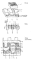
- FIG. 1 shows the cell construction
- FIG. 1b shows the cell layout
- FIG. 1c shows the cross section
- FIG. 2a shows the cell construction
- FIG. 2b shows the cell layout
- FIG. 2c the cross section
- CMOS wells are formed in a p-doped silicon substrate with a LOGOS process field isolation areas and active areas and then LDD-MOS transistors, consisting of isolated polysilicon word lines 12 with silicon dioxide cover insulation, lateral insulation spacers and source 7 and drain regions 9.
- a 400 nm thick, rounded lower insulation layer 11 is then applied and structured, as a result of which source contact windows 8 are opened in the memory matrix.
- the bit line is then generated and connected by deposition, doping and structuring of a polycid layer.
- a 650 nm thick top layer 13, rounded by means of RTA, is applied (FIG. 4a) and with a RIE process via a resist mask in the drain regions 9 of the n-LDD-MOS transistors of the Spelcher matrix, steep-sided drain contact window 10 with a minimal contact window width of 1.0 ⁇ m was introduced into the upper insulation layer 13, the etching process being stopped by its selectivity with respect to the bit line material on the bit line surface.
- Another RIE process cuts through the bit line 6 exposed in the drain contact window 10, the lower insulation layer 11 being etched to a remaining thickness of 200 nm.
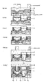
- a 20 nm thick, phosphorus-doped polysilicon layer is deposited. Then a 200 nm thick tungsten CVD layer conformally covering the steep flanks of the drain contact window 10 is applied (FIG. 4b) and removed again from all horizontal surfaces by a subsequent anisotropic RIE process. However, on the steep flanks of the drain contact window 10, the double layer consisting of tungsten and polysilicon remains in the form of a conductive ring 16. The conductive ring 16 contacts and closes the bit line 6 broken through the drain contact window etching process except for that in the center of the conductive Ring's remaining drain contact window 10 again.
- the upper insulation layer 13 is removed over a large area and, in the region of the remaining drain contact window 10, the lower insulation layer 11 is also removed by approximately 50 nm.
- a thin insulation layer 20 in the form of a 50 nm thick silicon nitride layer is deposited by means of an LPCVD process and removed from the horizontal surfaces by an anisotropic RIE etching process, the silicon nitride layer 20 remaining on the inner horizontal wall surface of the conductive ring 16 obtained with unattenuated thickness (Fig. 4c).
- the exposed upper cover surface of the conductive ring 16 is then isotropically and selectively etched down to a level of approximately 200 nm above the bit line surface, the silicon nitride layer 20 on the inner vertical wall surface of the conductive ring 16 being completely retained.
- a 140 nm thick silicon layer is then deposited using an LPCVD process (FIG. 4d) and then removed again on all horizontal surfaces by an anisotropic RIE process.
- the drain contact window 10 remaining in the center of the conductive ring 16 is subsequently opened up to the substrate surface.
- the conductive ring 16 is thus covered on its upper cover surface and its inner vertical wall surface by an insulation jacket 15, which is formed from two mask-free structured silicon nitride layers.
- n-conductive polysilicon layer becomes the lowest bottom plate layer 2a, which contacts the drain region 9 and the drain contact window 10 remaining in the center of the conductive ring 16 and its insulation jacket 15 a conductive stamp 14 completely filled out, deposited.
- auxiliary insulator layer 17 is applied (FIG. 4e; FIG. 3b) and a steep-sided breakthrough with a width of 1 is applied via a lacquer mask with an anisotropic selective RIE process, which is stopped on the bottom base plate layer 2A , 6 ⁇ m are introduced into the auxiliary insulator layer 17.
- an n-conducting polysilicon layer with a thickness of 175 nm is deposited as the first conductive lamella layer, then a first thin auxiliary insulation layer 18 with a thickness of 180 nm is applied (FIG.
- the layer stack of all lamella layers lying on the surface of the thick auxiliary insulation layer 17 is then removed using an RIE process, the surfaces of the thick auxiliary insulation layer 17 and the thin auxiliary insulation layers 18 remaining in the steep-sided opening being exposed and the upper ends of the layers being arranged vertically in the opening Polysilicon lamellae 3 are separated from one another (FIG. 3f).
- the polysilicon lamellae 3 which are vertically free in the area of the previous steep-sided opening, are removed vertically by the anisotropic RIE method by the thickness of the lowest base plate layer 2A, the RIE -Procedure is stopped on the upper insulation layer 13.
- the self-aligning etching of the bottom floor slab layer 2A takes place in the area outside the previous steep-sided opening and thus the separation of the storage electrodes 1 of adjacent storage cells, the conductive floor slab 2 connecting the conductive lamellae horizontally, that of the bottom floor slab layer 2A and horizontal parts of the polysilicon lamella layers is thinned by the thickness of the lowermost base plate layer, but is not cut through (FIG. 3h).
- an ONO storage dielectric 4 with a silicon dioxide equivalent thickness of 3 nm is produced from a 3 nm thick polysilicon layer, a 10 nm thick LPCVD silicon nitride layer and a reoxidation of the silicon nitride layer.
- n-doped polysilicon layer is then deposited and structured as a cell plate 5 with a thickness of 150 nm, which completely fills the spaces between the polysilicon fins 3.
Landscapes
- Engineering & Computer Science (AREA)
- Physics & Mathematics (AREA)
- Condensed Matter Physics & Semiconductors (AREA)
- General Physics & Mathematics (AREA)
- Computer Hardware Design (AREA)
- Microelectronics & Electronic Packaging (AREA)
- Power Engineering (AREA)
- Manufacturing & Machinery (AREA)
- Semiconductor Memories (AREA)
- Dram (AREA)
Priority Applications (1)
| Application Number | Priority Date | Filing Date | Title |
|---|---|---|---|
| EP94101691A EP0600850B1 (fr) | 1990-02-23 | 1991-02-14 | Structure de cellule DRAM avec condensateur sur la ligne de bit et procédé de sa manufacture |
Applications Claiming Priority (2)
| Application Number | Priority Date | Filing Date | Title |
|---|---|---|---|
| DD338097A DD299990A5 (de) | 1990-02-23 | 1990-02-23 | Ein-Transistor-Speicherzellenanordnung und Verfahren zu deren Herstellung |
| DD338097 | 1990-02-23 |
Related Child Applications (2)
| Application Number | Title | Priority Date | Filing Date |
|---|---|---|---|
| EP94101691A Division EP0600850B1 (fr) | 1990-02-23 | 1991-02-14 | Structure de cellule DRAM avec condensateur sur la ligne de bit et procédé de sa manufacture |
| EP94101691.7 Division-Into | 1994-02-04 |
Publications (3)
| Publication Number | Publication Date |
|---|---|
| EP0443439A2 true EP0443439A2 (fr) | 1991-08-28 |
| EP0443439A3 EP0443439A3 (en) | 1991-10-02 |
| EP0443439B1 EP0443439B1 (fr) | 1995-10-18 |
Family
ID=5616632
Family Applications (2)
| Application Number | Title | Priority Date | Filing Date |
|---|---|---|---|
| EP94101691A Expired - Lifetime EP0600850B1 (fr) | 1990-02-23 | 1991-02-14 | Structure de cellule DRAM avec condensateur sur la ligne de bit et procédé de sa manufacture |
| EP91102082A Expired - Lifetime EP0443439B1 (fr) | 1990-02-23 | 1991-02-14 | Dispositif de mémoire comprenant un transistor et son procédé de fabrication |
Family Applications Before (1)
| Application Number | Title | Priority Date | Filing Date |
|---|---|---|---|
| EP94101691A Expired - Lifetime EP0600850B1 (fr) | 1990-02-23 | 1991-02-14 | Structure de cellule DRAM avec condensateur sur la ligne de bit et procédé de sa manufacture |
Country Status (4)
| Country | Link |
|---|---|
| EP (2) | EP0600850B1 (fr) |
| AT (1) | ATE129363T1 (fr) |
| DD (1) | DD299990A5 (fr) |
| DE (3) | DE59106693D1 (fr) |
Cited By (9)
| Publication number | Priority date | Publication date | Assignee | Title |
|---|---|---|---|---|
| GB2259187A (en) * | 1991-08-31 | 1993-03-03 | Samsung Electronics Co Ltd | Capacitors for semiconductor memory cells |
| GB2259406A (en) * | 1991-09-07 | 1993-03-10 | Samsung Electronics Co Ltd | Semiconductor memory device capacitors |
| US5274258A (en) * | 1991-01-30 | 1993-12-28 | Samsung Electronics Co., Ltd. | High density semiconductor memory device (MBC cell) |
| WO1994000877A1 (fr) * | 1992-06-30 | 1994-01-06 | Siemens Aktiengesellschaft | Procede de fabrication d'un condensateur de memorisation |
| WO1994001891A1 (fr) * | 1992-07-08 | 1994-01-20 | Siemens Aktiengesellschaft | Procede de fabrication de condensateurs de memorisation pour cellules dram |
| EP0595360A1 (fr) * | 1992-10-30 | 1994-05-04 | Nec Corporation | Procédé de fabrication d'un dispositif semiconducteur avec une électrode cylindrique |
| GB2279176A (en) * | 1991-05-23 | 1994-12-21 | Samsung Electronics Co Ltd | Dram cell capacitor |
| GB2297648A (en) * | 1991-08-31 | 1996-08-07 | Samsung Electronics Co Ltd | Capacitors for semiconductor memory cells |
| FR2761198A1 (fr) * | 1997-03-07 | 1998-09-25 | United Microelectronics Corp | Procede cmp de polysilicium destine a des structures de cellules dram a haute densite |
Families Citing this family (4)
| Publication number | Priority date | Publication date | Assignee | Title |
|---|---|---|---|---|
| KR940006587B1 (ko) * | 1991-05-23 | 1994-07-22 | 삼성전자 주식회사 | 디램셀의 캐패시터 제조방법 |
| US5150276A (en) * | 1992-01-24 | 1992-09-22 | Micron Technology, Inc. | Method of fabricating a vertical parallel cell capacitor having a storage node capacitor plate comprising a center fin effecting electrical communication between itself and parallel annular rings |
| KR950021644A (ko) * | 1993-12-31 | 1995-07-26 | 김주용 | 반도체 기억장치 및 그 제조방법 |
| KR0126640B1 (ko) * | 1994-05-07 | 1998-04-02 | 김주용 | 반도체소자 및 그 제조방법 |
Family Cites Families (9)
| Publication number | Priority date | Publication date | Assignee | Title |
|---|---|---|---|---|
| US4855801A (en) * | 1986-08-22 | 1989-08-08 | Siemens Aktiengesellschaft | Transistor varactor for dynamics semiconductor storage means |
| JP2702121B2 (ja) * | 1987-02-25 | 1998-01-21 | 日本電気株式会社 | 半導体記憶装置 |
| US4872050A (en) * | 1988-03-15 | 1989-10-03 | Mitsubishi Denki Kabushiki Kaisha | Interconnection structure in semiconductor device and manufacturing method of the same |
| JP2755591B2 (ja) * | 1988-03-25 | 1998-05-20 | 株式会社東芝 | 半導体記憶装置 |
| JPH01302851A (ja) * | 1988-05-31 | 1989-12-06 | Fujitsu Ltd | 半導体メモリのメモリセル構造 |
| JPH01302852A (ja) * | 1988-05-31 | 1989-12-06 | Fujitsu Ltd | 半導体メモリのメモリセル構造 |
| JPH01308069A (ja) * | 1988-06-07 | 1989-12-12 | Fujitsu Ltd | 半導体メモリのメモリセル構造 |
| DE3918924C2 (de) * | 1988-06-10 | 1996-03-21 | Mitsubishi Electric Corp | Herstellungsverfahren für eine Halbleiterspeichereinrichtung |
| JP2724209B2 (ja) * | 1989-06-20 | 1998-03-09 | シャープ株式会社 | 半導体メモリ素子の製造方法 |
-
1990
- 1990-02-23 DD DD338097A patent/DD299990A5/de unknown
-
1991
- 1991-02-14 DE DE59106693T patent/DE59106693D1/de not_active Expired - Fee Related
- 1991-02-14 EP EP94101691A patent/EP0600850B1/fr not_active Expired - Lifetime
- 1991-02-14 AT AT91102082T patent/ATE129363T1/de not_active IP Right Cessation
- 1991-02-14 EP EP91102082A patent/EP0443439B1/fr not_active Expired - Lifetime
- 1991-02-14 DE DE59109236T patent/DE59109236D1/de not_active Expired - Fee Related
- 1991-02-19 DE DE4105501A patent/DE4105501A1/de not_active Withdrawn
Cited By (15)
| Publication number | Priority date | Publication date | Assignee | Title |
|---|---|---|---|---|
| US5274258A (en) * | 1991-01-30 | 1993-12-28 | Samsung Electronics Co., Ltd. | High density semiconductor memory device (MBC cell) |
| GB2279176B (en) * | 1991-05-23 | 1995-06-07 | Samsung Electronics Co Ltd | DRAM cell capacitor |
| GB2279176A (en) * | 1991-05-23 | 1994-12-21 | Samsung Electronics Co Ltd | Dram cell capacitor |
| GB2259187B (en) * | 1991-08-31 | 1996-06-19 | Samsung Electronics Co Ltd | Semiconductor device |
| US5330614A (en) * | 1991-08-31 | 1994-07-19 | Samsung Electronics Co., Ltd. | Manufacturing method of a capacitor having a storage electrode whose sidewall is positively inclined with respect to the horizontal surface |
| FR2680913A1 (fr) * | 1991-08-31 | 1993-03-05 | Samsung Electronics Co Ltd | Dispositif de memoire a semiconducteur ayant un condensateur et procede pour sa fabrication. |
| GB2259187A (en) * | 1991-08-31 | 1993-03-03 | Samsung Electronics Co Ltd | Capacitors for semiconductor memory cells |
| GB2297648A (en) * | 1991-08-31 | 1996-08-07 | Samsung Electronics Co Ltd | Capacitors for semiconductor memory cells |
| GB2297648B (en) * | 1991-08-31 | 1996-10-23 | Samsung Electronics Co Ltd | Semiconductor device |
| GB2259406B (en) * | 1991-09-07 | 1996-05-01 | Samsung Electronics Co Ltd | Semiconductor memory devices |
| GB2259406A (en) * | 1991-09-07 | 1993-03-10 | Samsung Electronics Co Ltd | Semiconductor memory device capacitors |
| WO1994000877A1 (fr) * | 1992-06-30 | 1994-01-06 | Siemens Aktiengesellschaft | Procede de fabrication d'un condensateur de memorisation |
| WO1994001891A1 (fr) * | 1992-07-08 | 1994-01-20 | Siemens Aktiengesellschaft | Procede de fabrication de condensateurs de memorisation pour cellules dram |
| EP0595360A1 (fr) * | 1992-10-30 | 1994-05-04 | Nec Corporation | Procédé de fabrication d'un dispositif semiconducteur avec une électrode cylindrique |
| FR2761198A1 (fr) * | 1997-03-07 | 1998-09-25 | United Microelectronics Corp | Procede cmp de polysilicium destine a des structures de cellules dram a haute densite |
Also Published As
| Publication number | Publication date |
|---|---|
| ATE129363T1 (de) | 1995-11-15 |
| DE59106693D1 (de) | 1995-11-23 |
| DE59109236D1 (de) | 2002-07-04 |
| DE4105501A1 (de) | 1991-08-29 |
| EP0443439B1 (fr) | 1995-10-18 |
| EP0600850B1 (fr) | 2002-05-29 |
| EP0443439A3 (en) | 1991-10-02 |
| EP0600850A1 (fr) | 1994-06-08 |
| DD299990A5 (de) | 1992-05-14 |
Similar Documents
| Publication | Publication Date | Title |
|---|---|---|
| DE102004003315B4 (de) | Halbleitervorrichtung mit elektrischem Kontakt und Verfahren zur Herstellung derselben | |
| DE3788499T2 (de) | Halbleiter-Grabenkondensator-Struktur. | |
| DE4016686C2 (de) | Verfahren zum Herstellen eines Halbleiterspeichers | |
| DE3525418A1 (de) | Halbleiterspeichereinrichtung und verfahren zu ihrer herstellung | |
| DE3785317T2 (de) | Matrix hoher Packungsdichte aus dynamischen VMOS RAM. | |
| DE4028488A1 (de) | Halbleiterspeichervorrichtung und verfahren zu ihrer herstellung | |
| DE4126046A1 (de) | Herstellungsverfahren und struktur eines dram-speicherzellenkondensators | |
| EP0936673B1 (fr) | Réseau de cellules de mémoire et procédé de fabrication | |
| DE10128718B4 (de) | Grabenkondensator einer DRAM-Speicherzelle mit metallischem Collarbereich und nicht-metallischer Leitungsbrücke zum Auswahltransistor | |
| EP0875937A2 (fr) | Réseau de cellules DRAM et son procédé de fabrication | |
| EP0443439A2 (fr) | Dispositif de mémoire comprenant un transistor et son procédé de fabrication | |
| DE4029256A1 (de) | Stapelkondensator einer dram-speicherzelle und verfahren zu seiner herstellung | |
| EP0987753A2 (fr) | Condensateur empilé de type DRAM à aileron et son procédé de manufacture | |
| EP1125328B1 (fr) | Procede de production d'un ensemble de cellules de memoire ram dynamique | |
| DE19706533A1 (de) | Halbleitereinrichtung und Herstellungsverfahren derselben | |
| EP0945901A1 (fr) | Réseau de cellules DRAM à transistor vertical et son procédé de fabrication | |
| DE19832095C1 (de) | Stapelkondensator-Herstellungsverfahren | |
| DE19929211B4 (de) | Verfahren zur Herstellung eines MOS-Transistors sowie einer DRAM-Zellenanordung | |
| DE4203565A1 (de) | Dram und verfahren zu dessen herstellung | |
| DE10334547B4 (de) | Herstellungsverfahren für einen Grabenkondensator mit einem Isolationskragen, der über einen vergrabenen Kontakt einseitig mit einem Substrat elektrisch verbunden ist | |
| DE10239488A1 (de) | Prozessfluss für zweistufige Kragen-in-DRAM-Herstellung | |
| EP0399060B1 (fr) | Dispositif de mémoire semi-conductrice comprenant des condensateurs avec deux électrodes disposées dans une tranchée et son procédé de fabrication | |
| WO2000060666A1 (fr) | Ensemble cellules memoires et son procede de production | |
| DD280851A1 (de) | Verfahren zur herstellung von graben-speicherzellen | |
| DE10333777B4 (de) | Herstellungsverfahren für einen Grabenkondensator mit einem Isolationskragen, der über einen vergrabenen Kontakt einseitig mit einem Substrat elektrisch verbunden ist, insbesondere für eine Halbleiterspeicherzelle |
Legal Events
| Date | Code | Title | Description |
|---|---|---|---|
| PUAI | Public reference made under article 153(3) epc to a published international application that has entered the european phase |
Free format text: ORIGINAL CODE: 0009012 |
|
| PUAL | Search report despatched |
Free format text: ORIGINAL CODE: 0009013 |
|
| AK | Designated contracting states |
Kind code of ref document: A2 Designated state(s): AT CH DE FR GB IT LI NL |
|
| AK | Designated contracting states |
Kind code of ref document: A3 Designated state(s): AT CH DE FR GB IT LI NL |
|
| 17P | Request for examination filed |
Effective date: 19911017 |
|
| RAP1 | Party data changed (applicant data changed or rights of an application transferred) |
Owner name: INSTITUT FUER HALBLEITERPHYSIK FRANKFURT (ODER) GM |
|
| 17Q | First examination report despatched |
Effective date: 19930827 |
|
| GRAA | (expected) grant |
Free format text: ORIGINAL CODE: 0009210 |
|
| AK | Designated contracting states |
Kind code of ref document: B1 Designated state(s): AT CH DE FR GB IT LI NL |
|
| PG25 | Lapsed in a contracting state [announced via postgrant information from national office to epo] |
Ref country code: IT Free format text: LAPSE BECAUSE OF FAILURE TO SUBMIT A TRANSLATION OF THE DESCRIPTION OR TO PAY THE FEE WITHIN THE PRE;WARNING: LAPSES OF ITALIAN PATENTS WITH EFFECTIVE DATE BEFORE 2007 MAY HAVE OCCURRED AT ANY TIME BEFORE 2007. THE CORRECT EFFECTIVE DATE MAY BE DIFFERENT FROM THE ONE RECORDED.SCRIBED TIME-LIMIT Effective date: 19951018 Ref country code: NL Free format text: LAPSE BECAUSE OF FAILURE TO SUBMIT A TRANSLATION OF THE DESCRIPTION OR TO PAY THE FEE WITHIN THE PRESCRIBED TIME-LIMIT Effective date: 19951018 |
|
| REF | Corresponds to: |
Ref document number: 129363 Country of ref document: AT Date of ref document: 19951115 Kind code of ref document: T |
|
| XX | Miscellaneous (additional remarks) |
Free format text: TEILANMELDUNG 94101691.7 EINGEREICHT AM 14/02/91. |
|
| REF | Corresponds to: |
Ref document number: 59106693 Country of ref document: DE Date of ref document: 19951123 |
|
| PG25 | Lapsed in a contracting state [announced via postgrant information from national office to epo] |
Ref country code: GB Effective date: 19960214 |
|
| REG | Reference to a national code |
Ref country code: CH Ref legal event code: NV Representative=s name: A. BRAUN, BRAUN, HERITIER, ESCHMANN AG PATENTANWAE |
|
| ET | Fr: translation filed | ||
| NLV1 | Nl: lapsed or annulled due to failure to fulfill the requirements of art. 29p and 29m of the patents act | ||
| GBV | Gb: ep patent (uk) treated as always having been void in accordance with gb section 77(7)/1977 [no translation filed] |
Effective date: 19951213 |
|
| GBT | Gb: translation of ep patent filed (gb section 77(6)(a)/1977) |
Effective date: 19960524 |
|
| PLBE | No opposition filed within time limit |
Free format text: ORIGINAL CODE: 0009261 |
|
| STAA | Information on the status of an ep patent application or granted ep patent |
Free format text: STATUS: NO OPPOSITION FILED WITHIN TIME LIMIT |
|
| GBPC | Gb: european patent ceased through non-payment of renewal fee |
Effective date: 19960214 |
|
| 26N | No opposition filed | ||
| REG | Reference to a national code |
Ref country code: CH Ref legal event code: PUE Owner name: INSTITUT FUER HALBLEITERPHYSIK FRANKFURT (ODER) GM Ref country code: CH Ref legal event code: NV Representative=s name: SIEMENS SCHWEIZ AG |
|
| REG | Reference to a national code |
Ref country code: FR Ref legal event code: TP |
|
| PGFP | Annual fee paid to national office [announced via postgrant information from national office to epo] |
Ref country code: CH Payment date: 20010511 Year of fee payment: 11 |
|
| PGFP | Annual fee paid to national office [announced via postgrant information from national office to epo] |
Ref country code: AT Payment date: 20020123 Year of fee payment: 12 |
|
| PG25 | Lapsed in a contracting state [announced via postgrant information from national office to epo] |
Ref country code: CH Free format text: LAPSE BECAUSE OF NON-PAYMENT OF DUE FEES Effective date: 20020228 Ref country code: LI Free format text: LAPSE BECAUSE OF NON-PAYMENT OF DUE FEES Effective date: 20020228 |
|
| REG | Reference to a national code |
Ref country code: CH Ref legal event code: PL |
|
| PG25 | Lapsed in a contracting state [announced via postgrant information from national office to epo] |
Ref country code: AT Free format text: LAPSE BECAUSE OF NON-PAYMENT OF DUE FEES Effective date: 20030214 |
|
| PGFP | Annual fee paid to national office [announced via postgrant information from national office to epo] |
Ref country code: DE Payment date: 20050421 Year of fee payment: 15 |
|
| PGFP | Annual fee paid to national office [announced via postgrant information from national office to epo] |
Ref country code: FR Payment date: 20060216 Year of fee payment: 16 |
|
| PG25 | Lapsed in a contracting state [announced via postgrant information from national office to epo] |
Ref country code: DE Free format text: LAPSE BECAUSE OF NON-PAYMENT OF DUE FEES Effective date: 20060901 |
|
| REG | Reference to a national code |
Ref country code: FR Ref legal event code: ST Effective date: 20071030 |
|
| PG25 | Lapsed in a contracting state [announced via postgrant information from national office to epo] |
Ref country code: FR Free format text: LAPSE BECAUSE OF NON-PAYMENT OF DUE FEES Effective date: 20070228 |