EP0422613B1 - Liquid crystal device - Google Patents
Liquid crystal device Download PDFInfo
- Publication number
- EP0422613B1 EP0422613B1 EP90119418A EP90119418A EP0422613B1 EP 0422613 B1 EP0422613 B1 EP 0422613B1 EP 90119418 A EP90119418 A EP 90119418A EP 90119418 A EP90119418 A EP 90119418A EP 0422613 B1 EP0422613 B1 EP 0422613B1
- Authority
- EP
- European Patent Office
- Prior art keywords
- liquid crystal
- compound
- antiferroelectric liquid
- composition
- substrates
- Prior art date
- Legal status (The legal status is an assumption and is not a legal conclusion. Google has not performed a legal analysis and makes no representation as to the accuracy of the status listed.)
- Expired - Lifetime
Links
- 239000004973 liquid crystal related substance Substances 0.000 title claims description 78
- 150000001875 compounds Chemical class 0.000 claims description 62
- 239000000203 mixture Substances 0.000 claims description 54
- 239000000758 substrate Substances 0.000 claims description 21
- 125000004432 carbon atom Chemical group C* 0.000 claims description 14
- 125000003545 alkoxy group Chemical group 0.000 claims description 8
- 125000000547 substituted alkyl group Chemical group 0.000 claims description 8
- 239000011159 matrix material Substances 0.000 claims description 7
- 229910052799 carbon Inorganic materials 0.000 claims description 5
- 229910052731 fluorine Chemical group 0.000 claims description 5
- 125000001153 fluoro group Chemical group F* 0.000 claims description 5
- 125000004435 hydrogen atom Chemical group [H]* 0.000 claims description 5
- 239000007788 liquid Substances 0.000 claims description 3
- 229910052739 hydrogen Inorganic materials 0.000 claims description 2
- 239000001257 hydrogen Substances 0.000 claims description 2
- 239000012071 phase Substances 0.000 description 35
- 238000000034 method Methods 0.000 description 19
- -1 4-methylhexyl Chemical group 0.000 description 18
- 239000010410 layer Substances 0.000 description 16
- 239000010408 film Substances 0.000 description 13
- 230000010287 polarization Effects 0.000 description 13
- 230000007704 transition Effects 0.000 description 9
- 125000000217 alkyl group Chemical group 0.000 description 8
- 230000002269 spontaneous effect Effects 0.000 description 8
- 239000010409 thin film Substances 0.000 description 6
- 0 CCCCCC(C)C(C)*C1CCC(*C(CC2)CCC2C2CCC(*)CC2)CC1 Chemical compound CCCCCC(C)C(C)*C1CCC(*C(CC2)CCC2C2CCC(*)CC2)CC1 0.000 description 5
- 239000004990 Smectic liquid crystal Substances 0.000 description 5
- 210000002858 crystal cell Anatomy 0.000 description 5
- VYPSYNLAJGMNEJ-UHFFFAOYSA-N Silicium dioxide Chemical compound O=[Si]=O VYPSYNLAJGMNEJ-UHFFFAOYSA-N 0.000 description 4
- 238000005229 chemical vapour deposition Methods 0.000 description 4
- 238000010586 diagram Methods 0.000 description 4
- 239000005262 ferroelectric liquid crystals (FLCs) Substances 0.000 description 4
- 229920001721 polyimide Polymers 0.000 description 4
- WKBOTKDWSSQWDR-UHFFFAOYSA-N Bromine atom Chemical group [Br] WKBOTKDWSSQWDR-UHFFFAOYSA-N 0.000 description 3
- 210000004027 cell Anatomy 0.000 description 3
- 125000004093 cyano group Chemical group *C#N 0.000 description 3
- 239000011521 glass Substances 0.000 description 3
- 125000002496 methyl group Chemical group [H]C([H])([H])* 0.000 description 3
- 125000000449 nitro group Chemical group [O-][N+](*)=O 0.000 description 3
- 238000004544 sputter deposition Methods 0.000 description 3
- 125000006219 1-ethylpentyl group Chemical group [H]C([H])([H])C([H])([H])C([H])([H])C([H])([H])C([H])(*)C([H])([H])C([H])([H])[H] 0.000 description 2
- 125000004493 2-methylbut-1-yl group Chemical group CC(C*)CC 0.000 description 2
- 125000005917 3-methylpentyl group Chemical group 0.000 description 2
- SNRUBQQJIBEYMU-UHFFFAOYSA-N Dodecane Natural products CCCCCCCCCCCC SNRUBQQJIBEYMU-UHFFFAOYSA-N 0.000 description 2
- 239000005264 High molar mass liquid crystal Substances 0.000 description 2
- 239000004642 Polyimide Substances 0.000 description 2
- 229910004205 SiNX Inorganic materials 0.000 description 2
- 125000004429 atom Chemical group 0.000 description 2
- 125000000484 butyl group Chemical group [H]C([*])([H])C([H])([H])C([H])([H])C([H])([H])[H] 0.000 description 2
- 229910052681 coesite Inorganic materials 0.000 description 2
- 229910052906 cristobalite Inorganic materials 0.000 description 2
- 125000002704 decyl group Chemical group [H]C([H])([H])C([H])([H])C([H])([H])C([H])([H])C([H])([H])C([H])([H])C([H])([H])C([H])([H])C([H])([H])C([H])([H])* 0.000 description 2
- 238000000151 deposition Methods 0.000 description 2
- 230000008021 deposition Effects 0.000 description 2
- 238000005137 deposition process Methods 0.000 description 2
- 125000003438 dodecyl group Chemical group [H]C([H])([H])C([H])([H])C([H])([H])C([H])([H])C([H])([H])C([H])([H])C([H])([H])C([H])([H])C([H])([H])C([H])([H])C([H])([H])C([H])([H])* 0.000 description 2
- 125000001495 ethyl group Chemical group [H]C([H])([H])C([H])([H])* 0.000 description 2
- 125000003187 heptyl group Chemical group [H]C([*])([H])C([H])([H])C([H])([H])C([H])([H])C([H])([H])C([H])([H])C([H])([H])[H] 0.000 description 2
- 125000004051 hexyl group Chemical group [H]C([H])([H])C([H])([H])C([H])([H])C([H])([H])C([H])([H])C([H])([H])* 0.000 description 2
- 125000000959 isobutyl group Chemical group [H]C([H])([H])C([H])(C([H])([H])[H])C([H])([H])* 0.000 description 2
- 125000001449 isopropyl group Chemical group [H]C([H])([H])C([H])(*)C([H])([H])[H] 0.000 description 2
- 239000000463 material Substances 0.000 description 2
- 125000001400 nonyl group Chemical group [H]C([*])([H])C([H])([H])C([H])([H])C([H])([H])C([H])([H])C([H])([H])C([H])([H])C([H])([H])C([H])([H])[H] 0.000 description 2
- 125000002347 octyl group Chemical group [H]C([*])([H])C([H])([H])C([H])([H])C([H])([H])C([H])([H])C([H])([H])C([H])([H])C([H])([H])[H] 0.000 description 2
- 125000001147 pentyl group Chemical group C(CCCC)* 0.000 description 2
- 125000001436 propyl group Chemical group [H]C([*])([H])C([H])([H])C([H])([H])[H] 0.000 description 2
- 125000003548 sec-pentyl group Chemical group [H]C([H])([H])C([H])([H])C([H])([H])C([H])(*)C([H])([H])[H] 0.000 description 2
- 239000000377 silicon dioxide Substances 0.000 description 2
- 235000012239 silicon dioxide Nutrition 0.000 description 2
- 229910052682 stishovite Inorganic materials 0.000 description 2
- XOLBLPGZBRYERU-UHFFFAOYSA-N tin dioxide Chemical compound O=[Sn]=O XOLBLPGZBRYERU-UHFFFAOYSA-N 0.000 description 2
- 238000002834 transmittance Methods 0.000 description 2
- 229910052905 tridymite Inorganic materials 0.000 description 2
- 125000002023 trifluoromethyl group Chemical group FC(F)(F)* 0.000 description 2
- 125000002948 undecyl group Chemical group [H]C([*])([H])C([H])([H])C([H])([H])C([H])([H])C([H])([H])C([H])([H])C([H])([H])C([H])([H])C([H])([H])C([H])([H])C([H])([H])[H] 0.000 description 2
- UHOVQNZJYSORNB-UHFFFAOYSA-N Benzene Chemical group C1=CC=CC=C1 UHOVQNZJYSORNB-UHFFFAOYSA-N 0.000 description 1
- IKLNOINQWYDQGM-UHFFFAOYSA-N C1CC[IH]CC1 Chemical compound C1CC[IH]CC1 IKLNOINQWYDQGM-UHFFFAOYSA-N 0.000 description 1
- 239000004677 Nylon Substances 0.000 description 1
- 239000004372 Polyvinyl alcohol Substances 0.000 description 1
- JUJWROOIHBZHMG-UHFFFAOYSA-N Pyridine Chemical group C1=CC=NC=C1 JUJWROOIHBZHMG-UHFFFAOYSA-N 0.000 description 1
- PNEYBMLMFCGWSK-UHFFFAOYSA-N aluminium oxide Inorganic materials [O-2].[O-2].[O-2].[Al+3].[Al+3] PNEYBMLMFCGWSK-UHFFFAOYSA-N 0.000 description 1
- GPRLTFBKWDERLU-UHFFFAOYSA-N bicyclo[2.2.2]octane Chemical group C1CC2CCC1CC2 GPRLTFBKWDERLU-UHFFFAOYSA-N 0.000 description 1
- 230000005540 biological transmission Effects 0.000 description 1
- 230000015572 biosynthetic process Effects 0.000 description 1
- 229910052801 chlorine Inorganic materials 0.000 description 1
- 125000001309 chloro group Chemical group Cl* 0.000 description 1
- 238000000576 coating method Methods 0.000 description 1
- 239000000470 constituent Substances 0.000 description 1
- 229910052593 corundum Inorganic materials 0.000 description 1
- 239000013078 crystal Substances 0.000 description 1
- 125000004122 cyclic group Chemical group 0.000 description 1
- 125000000113 cyclohexyl group Chemical group [H]C1([H])C([H])([H])C([H])([H])C([H])(*)C([H])([H])C1([H])[H] 0.000 description 1
- ZUOUZKKEUPVFJK-UHFFFAOYSA-N diphenyl Chemical class C1=CC=CC=C1C1=CC=CC=C1 ZUOUZKKEUPVFJK-UHFFFAOYSA-N 0.000 description 1
- 230000005684 electric field Effects 0.000 description 1
- 238000010438 heat treatment Methods 0.000 description 1
- 238000007654 immersion Methods 0.000 description 1
- AMGQUBHHOARCQH-UHFFFAOYSA-N indium;oxotin Chemical compound [In].[Sn]=O AMGQUBHHOARCQH-UHFFFAOYSA-N 0.000 description 1
- 239000007791 liquid phase Substances 0.000 description 1
- 238000005259 measurement Methods 0.000 description 1
- 239000012528 membrane Substances 0.000 description 1
- 125000000956 methoxy group Chemical group [H]C([H])([H])O* 0.000 description 1
- 125000001624 naphthyl group Chemical group 0.000 description 1
- 229920001778 nylon Polymers 0.000 description 1
- 239000012044 organic layer Substances 0.000 description 1
- 239000011368 organic material Substances 0.000 description 1
- 238000010587 phase diagram Methods 0.000 description 1
- 229920002120 photoresistant polymer Polymers 0.000 description 1
- 229920001296 polysiloxane Polymers 0.000 description 1
- 229920002451 polyvinyl alcohol Polymers 0.000 description 1
- 235000019422 polyvinyl alcohol Nutrition 0.000 description 1
- 239000002243 precursor Substances 0.000 description 1
- 125000003373 pyrazinyl group Chemical group 0.000 description 1
- 125000000714 pyrimidinyl group Chemical group 0.000 description 1
- 229920005989 resin Polymers 0.000 description 1
- 239000011347 resin Substances 0.000 description 1
- 230000004044 response Effects 0.000 description 1
- 238000007650 screen-printing Methods 0.000 description 1
- 239000000565 sealant Substances 0.000 description 1
- 238000007789 sealing Methods 0.000 description 1
- 230000035939 shock Effects 0.000 description 1
- 125000006850 spacer group Chemical group 0.000 description 1
- 238000004528 spin coating Methods 0.000 description 1
- 239000000126 substance Substances 0.000 description 1
- 238000001771 vacuum deposition Methods 0.000 description 1
- 229910001845 yogo sapphire Inorganic materials 0.000 description 1
Images


Classifications
-
- G—PHYSICS
- G02—OPTICS
- G02F—OPTICAL DEVICES OR ARRANGEMENTS FOR THE CONTROL OF LIGHT BY MODIFICATION OF THE OPTICAL PROPERTIES OF THE MEDIA OF THE ELEMENTS INVOLVED THEREIN; NON-LINEAR OPTICS; FREQUENCY-CHANGING OF LIGHT; OPTICAL LOGIC ELEMENTS; OPTICAL ANALOGUE/DIGITAL CONVERTERS
- G02F1/00—Devices or arrangements for the control of the intensity, colour, phase, polarisation or direction of light arriving from an independent light source, e.g. switching, gating or modulating; Non-linear optics
- G02F1/01—Devices or arrangements for the control of the intensity, colour, phase, polarisation or direction of light arriving from an independent light source, e.g. switching, gating or modulating; Non-linear optics for the control of the intensity, phase, polarisation or colour
- G02F1/13—Devices or arrangements for the control of the intensity, colour, phase, polarisation or direction of light arriving from an independent light source, e.g. switching, gating or modulating; Non-linear optics for the control of the intensity, phase, polarisation or colour based on liquid crystals, e.g. single liquid crystal display cells
-
- C—CHEMISTRY; METALLURGY
- C09—DYES; PAINTS; POLISHES; NATURAL RESINS; ADHESIVES; COMPOSITIONS NOT OTHERWISE PROVIDED FOR; APPLICATIONS OF MATERIALS NOT OTHERWISE PROVIDED FOR
- C09K—MATERIALS FOR MISCELLANEOUS APPLICATIONS, NOT PROVIDED FOR ELSEWHERE
- C09K19/00—Liquid crystal materials
- C09K19/04—Liquid crystal materials characterised by the chemical structure of the liquid crystal components, e.g. by a specific unit
- C09K19/42—Mixtures of liquid crystal compounds covered by two or more of the preceding groups C09K19/06 - C09K19/40
- C09K19/46—Mixtures of liquid crystal compounds covered by two or more of the preceding groups C09K19/06 - C09K19/40 containing esters
-
- G—PHYSICS
- G09—EDUCATION; CRYPTOGRAPHY; DISPLAY; ADVERTISING; SEALS
- G09G—ARRANGEMENTS OR CIRCUITS FOR CONTROL OF INDICATING DEVICES USING STATIC MEANS TO PRESENT VARIABLE INFORMATION
- G09G3/00—Control arrangements or circuits, of interest only in connection with visual indicators other than cathode-ray tubes
- G09G3/20—Control arrangements or circuits, of interest only in connection with visual indicators other than cathode-ray tubes for presentation of an assembly of a number of characters, e.g. a page, by composing the assembly by combination of individual elements arranged in a matrix no fixed position being assigned to or needed to be assigned to the individual characters or partial characters
- G09G3/34—Control arrangements or circuits, of interest only in connection with visual indicators other than cathode-ray tubes for presentation of an assembly of a number of characters, e.g. a page, by composing the assembly by combination of individual elements arranged in a matrix no fixed position being assigned to or needed to be assigned to the individual characters or partial characters by control of light from an independent source
- G09G3/36—Control arrangements or circuits, of interest only in connection with visual indicators other than cathode-ray tubes for presentation of an assembly of a number of characters, e.g. a page, by composing the assembly by combination of individual elements arranged in a matrix no fixed position being assigned to or needed to be assigned to the individual characters or partial characters by control of light from an independent source using liquid crystals
- G09G3/3611—Control of matrices with row and column drivers
- G09G3/3622—Control of matrices with row and column drivers using a passive matrix
- G09G3/3629—Control of matrices with row and column drivers using a passive matrix using liquid crystals having memory effects, e.g. ferroelectric liquid crystals
- G09G3/3633—Control of matrices with row and column drivers using a passive matrix using liquid crystals having memory effects, e.g. ferroelectric liquid crystals with transmission/voltage characteristic comprising multiple loops, e.g. antiferroelectric liquid crystals
-
- G—PHYSICS
- G02—OPTICS
- G02F—OPTICAL DEVICES OR ARRANGEMENTS FOR THE CONTROL OF LIGHT BY MODIFICATION OF THE OPTICAL PROPERTIES OF THE MEDIA OF THE ELEMENTS INVOLVED THEREIN; NON-LINEAR OPTICS; FREQUENCY-CHANGING OF LIGHT; OPTICAL LOGIC ELEMENTS; OPTICAL ANALOGUE/DIGITAL CONVERTERS
- G02F1/00—Devices or arrangements for the control of the intensity, colour, phase, polarisation or direction of light arriving from an independent light source, e.g. switching, gating or modulating; Non-linear optics
- G02F1/01—Devices or arrangements for the control of the intensity, colour, phase, polarisation or direction of light arriving from an independent light source, e.g. switching, gating or modulating; Non-linear optics for the control of the intensity, phase, polarisation or colour
- G02F1/13—Devices or arrangements for the control of the intensity, colour, phase, polarisation or direction of light arriving from an independent light source, e.g. switching, gating or modulating; Non-linear optics for the control of the intensity, phase, polarisation or colour based on liquid crystals, e.g. single liquid crystal display cells
- G02F1/137—Devices or arrangements for the control of the intensity, colour, phase, polarisation or direction of light arriving from an independent light source, e.g. switching, gating or modulating; Non-linear optics for the control of the intensity, phase, polarisation or colour based on liquid crystals, e.g. single liquid crystal display cells characterised by the electro-optical or magneto-optical effect, e.g. field-induced phase transition, orientation effect, guest-host interaction or dynamic scattering
- G02F1/139—Devices or arrangements for the control of the intensity, colour, phase, polarisation or direction of light arriving from an independent light source, e.g. switching, gating or modulating; Non-linear optics for the control of the intensity, phase, polarisation or colour based on liquid crystals, e.g. single liquid crystal display cells characterised by the electro-optical or magneto-optical effect, e.g. field-induced phase transition, orientation effect, guest-host interaction or dynamic scattering based on orientation effects in which the liquid crystal remains transparent
- G02F1/141—Devices or arrangements for the control of the intensity, colour, phase, polarisation or direction of light arriving from an independent light source, e.g. switching, gating or modulating; Non-linear optics for the control of the intensity, phase, polarisation or colour based on liquid crystals, e.g. single liquid crystal display cells characterised by the electro-optical or magneto-optical effect, e.g. field-induced phase transition, orientation effect, guest-host interaction or dynamic scattering based on orientation effects in which the liquid crystal remains transparent using ferroelectric liquid crystals
- G02F1/1412—Antiferroelectric liquid crystals
-
- G—PHYSICS
- G09—EDUCATION; CRYPTOGRAPHY; DISPLAY; ADVERTISING; SEALS
- G09G—ARRANGEMENTS OR CIRCUITS FOR CONTROL OF INDICATING DEVICES USING STATIC MEANS TO PRESENT VARIABLE INFORMATION
- G09G2310/00—Command of the display device
- G09G2310/06—Details of flat display driving waveforms
-
- G—PHYSICS
- G09—EDUCATION; CRYPTOGRAPHY; DISPLAY; ADVERTISING; SEALS
- G09G—ARRANGEMENTS OR CIRCUITS FOR CONTROL OF INDICATING DEVICES USING STATIC MEANS TO PRESENT VARIABLE INFORMATION
- G09G2320/00—Control of display operating conditions
- G09G2320/02—Improving the quality of display appearance
- G09G2320/0209—Crosstalk reduction, i.e. to reduce direct or indirect influences of signals directed to a certain pixel of the displayed image on other pixels of said image, inclusive of influences affecting pixels in different frames or fields or sub-images which constitute a same image, e.g. left and right images of a stereoscopic display
Definitions
- This invention relates to a liquid crystal device, and more particularly to a liquid crystal device comprising an antiferroelectric liquid crystal composition showing tristable switching.
- a ferroelectric liquid crystal display device using a ferroelectric liquid crystal such as of chiral smectic C phase has been investigated (See N.A. Clark, et al, Appl.Phys. Left., 36, 899 (1980)).
- the display device has a wide view angle and permits a large capacity display of more than 1000 x 1000 lines, so that it has been expected to be promising.
- the device has such problem that good orientation and memory characteristic required for the display device cannot be readily realized in a practical cell and is likely to be influenced by a shock from the outside.
- the display device has to settle many tasks for realization.
- the newly found liquid crystal phase is not yet fully clarified and is expressed in various manner by investigators, for example, S Y * phase (Japanese Unexamined Patent Publication HEI 1-213390/1989) or SmC A * (Fukuda, the Japan Society for the Promotion of Science Information science organic materials, 142th Committee, 45th joint research materials, 34(1989)).
- the phase may be regarded as an antiferroelectric smectic phase having a helical structure wherein the long axes of molecules are tilted with respect to the layer plane.
- a molecular arrangement to cause dipoles to be canceled in each layer,as shown in Fig.1(a).
- dipoles may be changed in molecular arrangement to be aligned with each other along the direction of voltage as shown in Figs.1(b) or 1(c).
- polarizing plates can be combined with the device to realize a bright or dark display.
- the relationship between the applied voltage and the tilt angle is as shown in Fig. 2, wherein three stable states 1 to 3 can be taken to draw a hysteresis curve. Therefore, the relationship may be used for driving liquid crystal display device.
- liquid crystal devices Although not impossible to produce liquid crystal devices by using a single compound which shows the above antiferroelectric liquid crystal phase, such liquid crystal devices are not fully satisfactory in that the temperature range showing tristable switching is narrow and a relatively higher voltage is required for controlling the switching.
- the present invention has been accomplished under the foregoing situations, and an object thereof is to provide a liquid crystal device using an antiferroelectric liquid crystal composition that shows a switching characteristic at low voltage.
- a liquid crystal device which comprises a pair of substrates each provided with a voltage applying means, an orientation control layer disposed on at least one of the pair of substrates, and an antiferroelectric liquid crystal layer disposed between the pair of substrates, the antiferroelectric liquid crystal layer comprising a liquid crystal composition including at least one compound represented by the following general formula (1): wherein R1 represents an optionally substituted alkyl or alkoxy group, having 1 to 15 carbon atoms, R2 represents an optionally substituted alkyl group having 1 to 15 carbon atoms, X represents a hydrogen or fluorine atom, m and n independently represent an integer 1 or 2, and * represents an asymmetric carbon atom , and at least one compound represented by the following general formula (II) : wherein R3 represents an optionally substituted alkyl or alkoxy group, having 1 to 15 carbon atoms, R4 represents an optionally substituted alkyl group, having 1 to 15 carbon atoms, represents X represents a
- Fig.1 is a diagram illustrating a molecular arrangement in an antiferroelectric liquid crystal phase.
- Fig. 2 is a diagram illustrating a relationship between the applied voltage and the tilt angle of an antiferroelectric liquid crystal.
- Fig. 3 is a sectional explanatory view showing a structure and a producing method of an antiferroelectric liquid crystal device of the present invention.
- Fig. 4 is a schematic view showing an example a matrix type antiferroelectric liquid crystal device of the invention.
- Figs. 5 to 7 are diagrams for explaining a method of driving a matrix type antiferroelectric liquid crystal device of the invention.
- Fig. 8 is a graph illustrating the polarization inverting current to be detected when a triangular wave voltage is applied to the antiferroelectric liquid crystal device of the present invention.
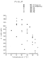
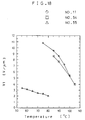
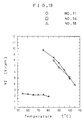
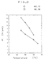
- Figs. 9 and 10 are graphs each illustrating the relation of switching voltage and temperature of the antiferroelectric liquid crystal device of the present invention.
- Fig. 11 is a graph showing the two-system phase diagram in relation to the mixture of the compound showing an antiferroelectric liquid crystal phase and those not showing the same.
- Figs.12 and 13 are graphs each illustrating the relation of switching voltage and temperature in the antiferroelectric liquid crystal device of the present invention.
- Fig. 14 is a graph illustrating a spontaneous polarization of an antiferroelectric liquid crystal composition used in the embodiment of the present invention.
- Figs.15 and 16 are graphs each illustrating the relation of switching voltage and temperature in the antiferroelectric liquid crystal device of the present invention.
- Fig. 17 is a diagram illustrating a spontaneous polarization of an antiferroelectric liquid crystal composition of used in the embodiment of the present invention.
- Figs.18 and 19 are graphs each illustrating the relation of switching voltage and temperature in the antiferroelectric liquid crystal device of the present invention.
- Fig. 20 is a graph illustrating a spontaneous polarization of an antiferroelectric liquid crystal composition used in the embodiment of the present invention.
- Figs.21 and 22 are graphs each illustrating the relation of switching voltage and temperature in the antiferroelectric liquid crystal device of the present invention.
- Fig. 23 is a graph illustrating a spontaneous polarization of an antiferroelectric liquid crystal composition used in the embodiment of the present invention.
- group R1 in the general formula (I) and the group R3 in the general formula (II) include various alkyl groups or alkoxy groups with straight or branched chains, respectively, and such alkyl groups include methyl, ethyl, propyl, i-propyl, butyl, i-butyl, pentyl, 1- or 2-methylbutyl, hexyl, 1- or 3-methylpentyl, heptyl, 1- or 4-methylhexyl, octyl, 1-methylheptyl, nonyl, 1- or 6-methyloctyl, decyl, 1-methynonyl, undecyl, 1-methyldecyl, dodecyl, 1-methylundecyl, and the like , and such alkoxy groups includes methoxy, ethoxy, propoxy, i-propoxy, butoxy, i-butoxy, pentoxy, 1- or 2-methylbutoxy, hexyloxy, 1-
- At least one hydrogen atom may be substituted with a fluorine atom, a chroline atom, a bromine atom, a cyano group, a trifluoromethyl group, or a nitro group.
- the alkyl or alkoxy group may contain an asymmetric carbon atom in the chain thereof.
- group R2 in the formula (I) and the group R4 in the formula (II) include various alkyl groups including methyl, ethyl, propyl, i-propyl, butyl, i-butyl, pentyl, 1-or 2-methylbutyl, hexyl, 1- or 3-methylpentyl, heptyl, 1- or 4-methylhexyl, octyl, 1-methylheptyl, nonyl, 1- or 6-methyloctyl, decyl, 1-methynonyl, undecyl, 1-methyldecyl, dodecyl, 1-methylundecyl and the like.
- At least one hydrogen atom may be substituted with a fluorine atom, a chroline atom, a bromine atom, a cyano group, a trifluoromethyl group, or a nitro group.
- the alkyl group may contain an asymmetric carbon atom in the chain thereof.
- Optically active compounds represented by the general formula (I) may be prepared, for example, by the method disclosed in Japanese Unexamined Patent Publication SHO 63-307837 (1988).
- the optically active compound shows an antiferroelectric liquid crystal phase by itself, but requires a higher voltage for switching, so that the optically active compound when solely used is practically tortured by many problems.
- mixing of the optically active compound represented by the general formula (I) with the compound represented by the general formula (II) as used in the present invention enables the voltage required for switching to lower.
- the mixture may contain suitably 30 to 99 wt%, preferably 50 to 90 wt%, of the compound represented by the general formula (I), and 1 to 70 wt%, preferably 10 to 50wt%, of that of the general formula (II).
- any compound other than those represented by the formulae (I) and (II) may be added in the above mixture at a proper quantity. This additional compound does not necessarily require to show a liquid crystal phase and examples thereof include the following compounds:
- R7 - Z1 - B1 - D1 - B2 - Z2 - R8 R7 - Z1 - B1 - D1 - B2 - D2 - B3 - Z2 - R8 wherein B1, B2, and B3 independently represent a six-membered cyclic ring such as benzen ring, cyclohexane ring, bicyclo[2.2.2]octane ring, pyridine ring, pyrimidine ring, pyrazine ring, dioxacyclohexane ring, and naphthalene ring, provided that the hydrogen atom in the ring may be substituted with a fluorine atom, a chlorine atom, a bromine atom, a cyano group,
- Z1 and Z2 each represents a single bond or a group of -COO-, -OCO-, -O-, -S-, -OCOO- or -CO-.
- R7 and R8 each represents an alkyl group with straight or branched chain having 1 to 15 carbon atoms which may contain an asymmetric carbon atom. s represents an integer of 1 or 2.
- the compound (c) may include the following compounds.
- an example of the antiferroelectric liquid crystal device of the present invention will be detailed.
- Fig. 3 is a sectional view illustrating an example of the antiferroelectric liquid crystal device of the present invention using an antiferroelectric liquid crystal composition.
- Fig. 3 shows an example of transmission type display device, wherein indicated at 1 is an insulating substrate; 2 is an conductive film; 3 is an insulating film; 4 is an orientation control layer; 5 is a sealant; 6 is an antiferroelectric liquid crystal composition; and 7 is a polarizer.
- Photo-transmissive substrate is used for the insulating substrate 1, and generally glass substrate is employed therefor.
- the conductive film 2 which is usually composed of a conductive thin film of InO3, SnO2 or ITO (Indium-tin oxide), is used as a transparent electrode and is formed with a predetermined pattern on the insulating substrate 1.
- the film 3 On the substrate is formed an insulating film 3, but the film 3 may be omitted in some cases.
- the insulating film 3 there may be used, for example, an inorganic thin film such as of SiO2, SiN X , Al2O3, etc., and an organic thin film such as of polyimide, photoresist resin, polymer liquid crystal, etc.
- the insulating film 3 is composed of an inorganic thin film, it may be formed by vacuum deposition process, sputtering process, CVD (Chemical Vapor Deposition) process or solution coating process.
- the insulating film 3 is composed of organic thin film
- it may be formed by using a solution dissolving an organic substance or a solution of its precursor according to spin-coating process, immersion application process, screen printing process, roller application process and curing it at a predetermined conditions (heating, photo-irradiation, etc); the thin film may also be formed by LB(Langumuir-Blodgett) process as well as deposition process, sputtering process, CVD process.
- an orientation control layer 4 On the insulating film 3 is formed an orientation control layer 4.
- the orientation control layer 4 may be directly on the conductive film 2.
- an inorganic layer may be used in some cases, while an organic layer may be also used in other cases.
- an inorganic orientation control layer slant deposition of silicone oxide is commonly conducted for the formation thereof. Rotating deposition may be also conducted.
- nylon, polyvinylalcohol, polyimide and the like may be used.
- rubbing treatment is usually effected on the layer.
- the orientation control layer can also be formed by using a polymer liquid crystal or LB membrane with an intended orientation, by using magnetic field orientating technique or by using spacer edge method.
- SiO2, SiN X and the like may be formed by deposition process, sputtering process, CVD process and the like, on which rubbing treatment is effected for providing the orientation control layer.
- the antiferroelectric liquid crystal device of the present invention may be also applied to a matrix type display device with a large capacity wherein the wiring (electrodes) on the upper substrate together with those on the substrate are intersectionally placed as to provide a matrix type device structure, as is shown in a plan schematic view of Fig.4.
- Fig.4 shows an example of a simple matrix device comprising 16 scanning electrodes 8 and 16 signal electrodes 9.
- the scanning electrodes 8 are labeled as L1, L2, L3 ,.... to L g from the uppermost one and the signal electrodes as S1, S2, S3, ... to S g from the left side.
- the intersection of the scanning electrode L i and the signal electrode S j is represented as a pixel A ij (i and j are positive integers).
- the scanning electrodes 8 of the simple matrix device are connected with a scanning side driver 10, and the signal electrodes 9 are connected with a signal side driver 11.
- Such a matrix-type liquid crystal device may be driven by the drive waveforms and the driving method as shown in Figs. 5 and 6. Specifically, at odd-numbered frames, a selection voltage waveform G shown in 1 of Fig.5 is sequentially applied to L1 through L g of the scanning electrodes 8, and at even-numbered frames the selection voltage waveform I shown in 3 of Fig.5 is sequentially applied to L1 through L g of the same. After application of the selection voltage waveform G of 1 to L i of the scanning electrode 8, non-selection voltage waveform H of 2 in Fig.5 is applied to L i of the scanning electrodes 8 in the same frame. While, after application of selection voltage waveform I of 3 of Fig.
- non-selection voltage waveform J of 4 of Fig. 5 is applied to L i of the scanning electrodes 8 in the same frame.
- ON voltage waveform of 5 in Fig.5 is to be applied to S j of the signal electrodes 9.
- OFF voltage waveform of 6 is to be applied to S j of the signal electrode 9.
- ON voltage waveform of 7 in Fig.5 is to be applied to S j of the signal electrode 9.
- OFF voltage waveform of 8 is to be applied to S j of the signal electrode 9.
- the polarization axis of the polarizing plate is made to match with a direction perpendicular to the smectic layer of in the state 2 of Fig. 2).
- Voltage waveforms applied to the scanning electrodes L a , L b , the signal electrodes S4, S c , and pixels A b4 , A bc when the pattern of Fig.4 is displayed by the above manner is shown in Fig. 6.
- the antiferroelectric liquid crystal makes response corresponding to applied voltage but substantially not to application time of voltage, so that there appears no crosstalk.
- a driving waveform shown in Fig.7 may be alternatively used instead of that of Fig. 5.
- a polyimide film was formed on each of the two glass substrates provided with ITO films. Rubbing treatment was effected on one of the substrates.
- the two substrates were opposedly placed to each other to provide a liquid crystal cell with a cell thickness of 3 ⁇ m.
- the liquid crystal compositions Nos. 31 and 32 were each injected in the liquid crystal cell which was then heated first to temperature that the liquid crystal composition changes to an isotropic liquid, and thereafter cooled to room temperature at a ratio of 1° C/min to obtain an antiferroelectric liquid crystal device of the invention.
- a triangular waveform voltage of 1Hz was applied to the antiferroelectric liquid crystal device to measure two polarization inverted current as shown in Fig. 8.
- the intensity of photo transmittance was measured under cross-nicol to obtain doubled hysteresis curve as shown in Fig.2 from which the threshold voltages V1 and V2 were calculated and plotted to the measured temperature to obtain the result shown in Figs. 9 and 10.
- the absolute values of the two voltages V1 and V2 mean switching voltages necessary for developing the states 1 and 2 of the liquid crystal phase as shown in Fig. 1.
- the phase transition temperature of the antiferroelectric liquid crystal compositions Nos 31 and 32 are shown in Table 3. TABLE 3 Liquid Crystal Materials Phase Transition Temperature (° C) C S CA * S A I Compound No.
- a liquid crystal device was fabricated in a similar manner to the first example excepting that the compound No.11 was simply used instead of the composition No.31 or 32 , and the measurement was effected as similar manner to the first example.
- the plots of V1 and V2 to the measured temperature are shown in Figs.9 and 10.
- the phase transition temperature of the antiferroelectric liquid crystal compound No.11 is also shown in Table 3. Comparing the first example of the present invention with the comparison example reveals that the device of the present invention realizes a lower voltage switching.
- compositions Nos.41 to 50 comprise the two constituents, the compounds Nos. 11 and 23, were prepared. The contents thereof are shown in Table 4. TABLE 4 Compositions Composition (mol. %) Compound No.11 Compound No.23 Composition No.41 88.7 11.3 Composition No.42 79.3 20.7 Composition No.43 75.4 24.6 Composition No.44 66.5 33.5 Composition No.45 60.1 39.9 Composition No.46 50.3 49.7 Composition No.47 40.0 60.0 Composition No.48 30.7 69.3 Composition No.49 18.2 81.8 Composition No.50 10.8 89.2
- a polyimide film was formed on each of the two glass substrates provided with ITO films. Rubbing treatment was effected on both of the substrates. The two substrates were opposedly placed to each other to provide a liquid crystal cell with a cell thickness of 5 ⁇ m.
- the liquid crystal compositions Nos. 41 to 50 were each injected in the liquid crystal cells which were then heated first to the temperature that the liquid crystal composition changes to an isotropic liquid, and thereafter cooled to room temperature at a ratio of 1° C/min to obtain an antiferroelectric liquid crystal device of the invention.
- a triangular waveform voltage of 0.02 Hz was applied to the antiferroelectric liquid crystal device to measure two polarization inverted current as shown in Fig. 8.
- the use of the compound No.23 enables the field strength necessary for switching to lower.
- compositions Nos. 43 and 51 to 54 were prepared by adding 25 mole% of a compound not showing an antiferroelectric liquid crystal phase to the compound No.11 showing an antiferroelectric liquid crystal phase.
- the compounds added and their phase transition temperature are as shown in Table 5.
- compositions as shown in Table 6 were prepared. Their phase transition temperature is shown in Table 6 in which also shown is the phase transition temperature of the compound No.13. TABLE 6 Compositions Content Phase Transition temperature (° C) S CA * S A I Composition No.55 Compound No.11 (50 mole%) ⁇ 93 ⁇ 166 ⁇ Compound No.27 (50 mole%) Compound No.13 ⁇ 64 ⁇ 83 ⁇ Composition No.56 Compound No.13 (75 mole%) ⁇ 70 ⁇ 113 ⁇ Compound No.23 (25 mole%)
- the field strength (voltage) necessary for switching can be lowered by the addition of the compound that does not show an antiferroelectric liquid crystal phase.
- an antiferroelectric liquid crystal device which can be driven at a lower voltage can be provided.
Landscapes
- Chemical & Material Sciences (AREA)
- Engineering & Computer Science (AREA)
- Crystallography & Structural Chemistry (AREA)
- Physics & Mathematics (AREA)
- General Physics & Mathematics (AREA)
- Theoretical Computer Science (AREA)
- Computer Hardware Design (AREA)
- Materials Engineering (AREA)
- Organic Chemistry (AREA)
- Nonlinear Science (AREA)
- Optics & Photonics (AREA)
- Liquid Crystal Substances (AREA)
- Liquid Crystal (AREA)
Applications Claiming Priority (2)
| Application Number | Priority Date | Filing Date | Title |
|---|---|---|---|
| JP265487/89 | 1989-10-11 | ||
| JP26548789 | 1989-10-11 |
Publications (3)
| Publication Number | Publication Date |
|---|---|
| EP0422613A2 EP0422613A2 (en) | 1991-04-17 |
| EP0422613A3 EP0422613A3 (en) | 1992-01-02 |
| EP0422613B1 true EP0422613B1 (en) | 1995-01-04 |
Family
ID=17417864
Family Applications (1)
| Application Number | Title | Priority Date | Filing Date |
|---|---|---|---|
| EP90119418A Expired - Lifetime EP0422613B1 (en) | 1989-10-11 | 1990-10-10 | Liquid crystal device |
Country Status (6)
| Country | Link |
|---|---|
| US (1) | US5108650A (OSRAM) |
| EP (1) | EP0422613B1 (OSRAM) |
| JP (1) | JP2792729B2 (OSRAM) |
| KR (1) | KR940011934B1 (OSRAM) |
| DE (1) | DE69015760T2 (OSRAM) |
| TW (1) | TW215455B (OSRAM) |
Families Citing this family (21)
| Publication number | Priority date | Publication date | Assignee | Title |
|---|---|---|---|---|
| JP2526085B2 (ja) * | 1988-02-22 | 1996-08-21 | チッソ株式会社 | 強誘電性液晶組成物および液晶表示素子 |
| EP0450595B1 (en) * | 1990-04-04 | 1995-03-01 | Mitsubishi Gas Chemical Company, Inc. | Liquid crystal compound and liquid crystal display device |
| JP2788667B2 (ja) * | 1990-05-25 | 1998-08-20 | 出光興産株式会社 | 高分子液晶組成物、それを用いた液晶光学素子及び液晶光学素子の駆動方法 |
| EP0466573B1 (en) * | 1990-07-13 | 1995-02-15 | Showa Shell Sekiyu Kabushiki Kaisha | Liquid crystal compositions |
| US5364561A (en) * | 1990-07-13 | 1994-11-15 | Showa Shell Sekiyu Kabushiki Kaisha | Liquid crystal compounds and liquid crystal compositions containing them |
| EP0484849B1 (en) * | 1990-11-05 | 1994-08-31 | Mitsubishi Gas Chemical Company, Inc. | Optically active alcohol, process for producing same and liquid crystal compound using same |
| JP3039571B2 (ja) * | 1991-06-04 | 2000-05-08 | 三菱瓦斯化学株式会社 | 液晶組成物 |
| JPH04359990A (ja) * | 1991-06-06 | 1992-12-14 | Mitsui Petrochem Ind Ltd | 液晶組成物、その用途およびその製造方法 |
| JP2937274B2 (ja) * | 1991-07-29 | 1999-08-23 | チッソ株式会社 | 反強誘電性液晶組成物 |
| JP2866518B2 (ja) * | 1992-01-17 | 1999-03-08 | シャープ株式会社 | 反強誘電性液晶素子の駆動方法 |
| US5609790A (en) * | 1992-02-04 | 1997-03-11 | Seiko Epson Corporation | Liquid crystal compositions |
| JPH05249435A (ja) * | 1992-03-03 | 1993-09-28 | Mitsubishi Gas Chem Co Inc | 反強誘電性液晶素子 |
| US5559620A (en) * | 1992-03-05 | 1996-09-24 | Casio Computer Co., Ltd. | Anti-ferroelectric liquid crystal display device with intersecting alignment film directions |
| JPH05271658A (ja) * | 1992-03-27 | 1993-10-19 | Chisso Corp | 反強誘電性液晶組成物 |
| JPH0632770A (ja) * | 1992-05-20 | 1994-02-08 | Showa Shell Sekiyu Kk | 反強誘電性液晶化合物 |
| DE69319032T2 (de) * | 1992-08-05 | 1998-10-08 | Mitsubishi Gas Chemical Co | Antiferroelektrische Flüssigkristallzusammensetzung sowie Flüssigkristallanzeigevorrichtung |
| DE69308427T2 (de) * | 1992-08-19 | 1997-08-21 | Mitsubishi Gas Chemical Co | Antiferroelektrischer Flüssigkristall und Flüssigkristallanzeigevorrichtung |
| US6288764B1 (en) * | 1996-06-25 | 2001-09-11 | Semiconductor Energy Laboratory Co., Ltd. | Display device or electronic device having liquid crystal display panel |
| JPH10204036A (ja) * | 1997-01-27 | 1998-08-04 | Mitsubishi Gas Chem Co Inc | 反強誘電性液晶化合物 |
| JP3028097B2 (ja) | 1997-04-11 | 2000-04-04 | 日本電気株式会社 | スメクティック液晶材料および液晶光学素子 |
| EP1356345A2 (en) * | 2000-06-23 | 2003-10-29 | The University of Akron | Electrically tunable microlens array containing li quid crystals |
Family Cites Families (9)
| Publication number | Priority date | Publication date | Assignee | Title |
|---|---|---|---|---|
| DE3587601T2 (de) * | 1984-10-18 | 1994-03-10 | Chisso Corp | Ferroelektrische chirale smektische Flüssigkristallzusammensetzung. |
| DE3627964C2 (de) * | 1985-08-26 | 2000-11-02 | Samsung Electronic Devices | Ferroelektrische kristallin-flüssige Derivate verzweigter acyclischer chiraler alpha-Chlorcarbonsäuren, Verfahren zu ihrer Herstellung und ihre Verwendung in Gemischen für schnell schaltende Displays in der Optoelektronik |
| JPH0819410B2 (ja) * | 1987-06-01 | 1996-02-28 | チッソ株式会社 | スメクチック液晶混合物 |
| JP2660551B2 (ja) * | 1987-07-28 | 1997-10-08 | キヤノン株式会社 | 光学活性化合物及びそれを含む液晶組成物、液晶素子 |
| US4921632A (en) * | 1987-08-26 | 1990-05-01 | Nec Corporation | Liquid crystal compounds and compositions |
| EP0327349B1 (en) * | 1988-02-02 | 1996-04-10 | Showa Shell Sekiyu Kabushiki Kaisha | Liquid crystal compounds |
| JP2526085B2 (ja) * | 1988-02-22 | 1996-08-21 | チッソ株式会社 | 強誘電性液晶組成物および液晶表示素子 |
| DE68919727T2 (de) * | 1988-03-09 | 1995-06-01 | Showa Shell Sekiyu | Dioxan-Flüssigkristallverbindungen. |
| JPH0269440A (ja) * | 1988-09-05 | 1990-03-08 | Canon Inc | 光学活性液晶性化合物、それを含む液晶組成物および液晶素子 |
-
1990
- 1990-10-08 JP JP2270702A patent/JP2792729B2/ja not_active Expired - Fee Related
- 1990-10-10 DE DE69015760T patent/DE69015760T2/de not_active Expired - Lifetime
- 1990-10-10 US US07/594,972 patent/US5108650A/en not_active Expired - Lifetime
- 1990-10-10 EP EP90119418A patent/EP0422613B1/en not_active Expired - Lifetime
- 1990-10-11 KR KR1019900016101A patent/KR940011934B1/ko not_active Expired - Lifetime
- 1990-10-11 TW TW079108534A patent/TW215455B/zh active
Non-Patent Citations (1)
| Title |
|---|
| LIQUID CRYSTALS, vol. 6, no. 2, TAYLOR & FRANCIS, LONDON, pages 167-174; Y. SUZUKI ET AL.: "New fluorine-containing ferroelectric liquid crystal compounds showing tristable switching" * |
Also Published As
| Publication number | Publication date |
|---|---|
| EP0422613A2 (en) | 1991-04-17 |
| KR940011934B1 (ko) | 1994-12-27 |
| TW215455B (OSRAM) | 1993-11-01 |
| US5108650A (en) | 1992-04-28 |
| JP2792729B2 (ja) | 1998-09-03 |
| EP0422613A3 (en) | 1992-01-02 |
| KR910008453A (ko) | 1991-05-31 |
| DE69015760D1 (de) | 1995-02-16 |
| JPH03223390A (ja) | 1991-10-02 |
| DE69015760T2 (de) | 1995-08-24 |
Similar Documents
| Publication | Publication Date | Title |
|---|---|---|
| EP0422613B1 (en) | Liquid crystal device | |
| US6171519B1 (en) | Ferroelectric liquid crystal mixture | |
| JP2001081466A (ja) | 高いコントラスト値を有するアクティブマトリックスディスプレイ | |
| EP1119595B1 (en) | Tristable liquid crystal display device | |
| Pesant et al. | Optical switching of chiral smectic C at room temperature | |
| KR100354351B1 (ko) | 액정조성물및이것을함유한액정소자 | |
| US5550664A (en) | Liquid crystal display device | |
| US5800736A (en) | Smectic liquid crystal composition and liquid crystal device | |
| JPH0718990B2 (ja) | 液晶セル | |
| US6007739A (en) | Liquid crystal compound, liquid crystal composition, and liquid crystal display device using the same | |
| JPH08157463A (ja) | 液晶性化合物、それを含有する液晶組成物、それを有する液晶素子及びそれらを用いた表示方法、液晶装置 | |
| JPH09241249A (ja) | 光学活性化合物、それを含有する液晶組成物、それを有する液晶素子及びそれらを用いた表示方法、表示装置 | |
| JP3054212B2 (ja) | ゲストホスト型液晶光学素子 | |
| JPH08109145A (ja) | エチニレン化合物、それを含有する液晶組成物、それを有する液晶素子及びそれらを用いた表示方法、表示装置 | |
| JP3575050B2 (ja) | 液晶組成物およびこれを含む液晶素子 | |
| JPH06157371A (ja) | 強誘電性液晶表示素子 | |
| JPH08151577A (ja) | 光学活性化合物、それを含有する液晶組成物、それを有する液晶素子、それらを用いた液晶装置及び表示方法 | |
| JPH0772442A (ja) | 光学活性化合物、それを含有する液晶組成物、それを有する液晶素子及びそれらを用いた表示方法、表示装置 | |
| JPH0565485A (ja) | 強誘電性液晶組成物および液晶素子 | |
| US5612440A (en) | Polymeric orientating material and ferroelectric liquid crystal display adopting the same | |
| JP4067288B2 (ja) | 液晶組成物および液晶素子 | |
| JP3633009B2 (ja) | 液晶材料およびこれを含む液晶素子 | |
| JPH0859629A (ja) | テトラヒドロキナゾリン化合物、それを含有する液晶組成物、それを有する液晶素子及びそれらを用いた表示方法、表示装置 | |
| JPH09221441A (ja) | 光学活性化合物、それを含有する液晶組成物、それを有する液晶素子及びそれらを用いた表示方法、表示装置 | |
| JPH08157397A (ja) | 液晶性化合物、それを含有する液晶組成物、それを有する液晶素子、それらを用いた液晶装置及び表示方法 |
Legal Events
| Date | Code | Title | Description |
|---|---|---|---|
| PUAI | Public reference made under article 153(3) epc to a published international application that has entered the european phase |
Free format text: ORIGINAL CODE: 0009012 |
|
| 17P | Request for examination filed |
Effective date: 19901010 |
|
| AK | Designated contracting states |
Kind code of ref document: A2 Designated state(s): DE FR GB NL |
|
| PUAL | Search report despatched |
Free format text: ORIGINAL CODE: 0009013 |
|
| AK | Designated contracting states |
Kind code of ref document: A3 Designated state(s): DE FR GB NL |
|
| 17Q | First examination report despatched |
Effective date: 19921120 |
|
| GRAA | (expected) grant |
Free format text: ORIGINAL CODE: 0009210 |
|
| AK | Designated contracting states |
Kind code of ref document: B1 Designated state(s): DE FR GB NL |
|
| REF | Corresponds to: |
Ref document number: 69015760 Country of ref document: DE Date of ref document: 19950216 |
|
| ET | Fr: translation filed | ||
| PLBE | No opposition filed within time limit |
Free format text: ORIGINAL CODE: 0009261 |
|
| STAA | Information on the status of an ep patent application or granted ep patent |
Free format text: STATUS: NO OPPOSITION FILED WITHIN TIME LIMIT |
|
| 26N | No opposition filed | ||
| PGFP | Annual fee paid to national office [announced via postgrant information from national office to epo] |
Ref country code: FR Payment date: 20001010 Year of fee payment: 11 |
|
| REG | Reference to a national code |
Ref country code: GB Ref legal event code: IF02 |
|
| PG25 | Lapsed in a contracting state [announced via postgrant information from national office to epo] |
Ref country code: FR Free format text: LAPSE BECAUSE OF NON-PAYMENT OF DUE FEES Effective date: 20020628 |
|
| REG | Reference to a national code |
Ref country code: FR Ref legal event code: ST |
|
| PGFP | Annual fee paid to national office [announced via postgrant information from national office to epo] |
Ref country code: DE Payment date: 20091008 Year of fee payment: 20 |
|
| PGFP | Annual fee paid to national office [announced via postgrant information from national office to epo] |
Ref country code: NL Payment date: 20091015 Year of fee payment: 20 |
|
| PGFP | Annual fee paid to national office [announced via postgrant information from national office to epo] |
Ref country code: GB Payment date: 20091007 Year of fee payment: 20 |
|
| REG | Reference to a national code |
Ref country code: NL Ref legal event code: V4 Effective date: 20101010 |
|
| REG | Reference to a national code |
Ref country code: GB Ref legal event code: PE20 Expiry date: 20101009 |
|
| PG25 | Lapsed in a contracting state [announced via postgrant information from national office to epo] |
Ref country code: NL Free format text: LAPSE BECAUSE OF EXPIRATION OF PROTECTION Effective date: 20101010 |
|
| PG25 | Lapsed in a contracting state [announced via postgrant information from national office to epo] |
Ref country code: GB Free format text: LAPSE BECAUSE OF EXPIRATION OF PROTECTION Effective date: 20101009 |
|
| PG25 | Lapsed in a contracting state [announced via postgrant information from national office to epo] |
Ref country code: DE Free format text: LAPSE BECAUSE OF EXPIRATION OF PROTECTION Effective date: 20101010 |