EP0409256B1 - Halbleiter-IC-Vorrichtung und deren Herstellungsverfahren - Google Patents
Halbleiter-IC-Vorrichtung und deren Herstellungsverfahren Download PDFInfo
- Publication number
- EP0409256B1 EP0409256B1 EP90113945A EP90113945A EP0409256B1 EP 0409256 B1 EP0409256 B1 EP 0409256B1 EP 90113945 A EP90113945 A EP 90113945A EP 90113945 A EP90113945 A EP 90113945A EP 0409256 B1 EP0409256 B1 EP 0409256B1
- Authority
- EP
- European Patent Office
- Prior art keywords
- cell
- wires
- power source
- dummy
- dummy wires
- Prior art date
- Legal status (The legal status is an assumption and is not a legal conclusion. Google has not performed a legal analysis and makes no representation as to the accuracy of the status listed.)
- Expired - Lifetime
Links
Images


Classifications
-
- H—ELECTRICITY
- H01—ELECTRIC ELEMENTS
- H01L—SEMICONDUCTOR DEVICES NOT COVERED BY CLASS H10
- H01L27/00—Devices consisting of a plurality of semiconductor or other solid-state components formed in or on a common substrate
-
- H—ELECTRICITY
- H01—ELECTRIC ELEMENTS
- H01L—SEMICONDUCTOR DEVICES NOT COVERED BY CLASS H10
- H01L23/00—Details of semiconductor or other solid state devices
- H01L23/52—Arrangements for conducting electric current within the device in operation from one component to another, i.e. interconnections, e.g. wires, lead frames
- H01L23/522—Arrangements for conducting electric current within the device in operation from one component to another, i.e. interconnections, e.g. wires, lead frames including external interconnections consisting of a multilayer structure of conductive and insulating layers inseparably formed on the semiconductor body
- H01L23/528—Geometry or layout of the interconnection structure
- H01L23/5286—Arrangements of power or ground buses
-
- H—ELECTRICITY
- H01—ELECTRIC ELEMENTS
- H01L—SEMICONDUCTOR DEVICES NOT COVERED BY CLASS H10
- H01L23/00—Details of semiconductor or other solid state devices
- H01L23/52—Arrangements for conducting electric current within the device in operation from one component to another, i.e. interconnections, e.g. wires, lead frames
- H01L23/522—Arrangements for conducting electric current within the device in operation from one component to another, i.e. interconnections, e.g. wires, lead frames including external interconnections consisting of a multilayer structure of conductive and insulating layers inseparably formed on the semiconductor body
- H01L23/5222—Capacitive arrangements or effects of, or between wiring layers
-
- H—ELECTRICITY
- H01—ELECTRIC ELEMENTS
- H01L—SEMICONDUCTOR DEVICES NOT COVERED BY CLASS H10
- H01L2924/00—Indexing scheme for arrangements or methods for connecting or disconnecting semiconductor or solid-state bodies as covered by H01L24/00
- H01L2924/0001—Technical content checked by a classifier
- H01L2924/0002—Not covered by any one of groups H01L24/00, H01L24/00 and H01L2224/00
Definitions
- the present invention relates to a semiconductor IC circuit device having dummy wires and a method for manufacturing the same, both of which are employed for a multi-layer type semiconductor integrated circuit to be formed by an automatic array connection system, such as a standard cell structure and a gate array structure.
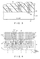
- Fig. 1 is a plan view showing an IC pattern having conventional dummy wires.
- reference numeral 1 shows a first connection layer; 2, a second connection layer; 3, a connection through hole or a contact hole; 4, dummy wires; 5, an array of cells (it is assumed that they are formed by a standard cell system); 6, an internal power source terminal V DD ; 7, an internal power source terminal V SS ; and 8, cell-to-cell wires.
- the conventional dummy wires has been proved ineffective in the case where they are employed to prevent an unevenness (a step) on the surface of integrated circuits and to offer a countermeasure against a loading effect, or to correct a wiring or connection error, if any.
- dummy wires 4 are used such that, as shown in Fig. 1, they have a proper width to serve the purpose for which they are formed.
- the dummy wires cannot be utilized in the conventional semiconductor. devices due in part to a "not fixed" width and in part to its own limited use in particular. If they are initially built in a semiconductor IC device so as to correct a connection error, they sometimes prove fruitless for'such a purpose as in the aforementioned case.
- GB-A-2 156 581 shows a DRAM with additional word lines at an end of the memory cell array, to protect the first active word line from being damaged during manufacture. A fixed potential is applied to the additional lines to prevent them floating.
- EP-A-210 397 shows conductor segments originally connected to power lines, being made available as signalling conductors in a standard cell layout for LSI circuits.
- Another object of the present invention is to provide a method for manufacturing the aforementioned semiconductor integrated circuit device.
- dummy wires are arranged, for example, in a multi-layer type semiconductor integrated circuit and connected to an internal power source potential V SS line.
- a capacitance is provided between the dummy wires and the integrated circuit's substrate, thus preventing an internal power source voltage fluctuation and supplying a stable voltage to an associated internal circuit.
- the dummy wires are arranged at the same pitch and width as those at which cell-to-cell wires are arranged and, if a semiconductor integrated circuit is found to be defective, are cut off the internal power source terminal line to correct a wrong connection layer or an improper signal delay time. It is, thus, possible to shorten a manufacturing step of the semiconductor integrated circuit.
- Figs. 2 and 3 are a plan view and cross-sectional view, respectively, showing a major section of the present embodiment.
- the same reference numerals are employed to designate a portion or an element corresponding to that shown in Fig. 1.
- reference numeral 1 shows a first connection layer; 2, a second connection layer; 3, a connection through-hole or a contact hole; 4, dummy wires; 5, an array of cells (it is assumed that an integral circuit is formed by a standard cell system); 6, an internal power source terminal V DD ; 7, an internal power source terminal V SS ; and 8, cell-to-cell wires.
- the first connection layer 1 to the right in Fig. 3 is composed of, for example, a first wire of aluminum and connected via the contact hole in the insulating film 32 to an N + type diffusion region 33 which is formed in the surface portion of the N type substrate 31.
- the second connection layer 2 to the right in Fig. 3 is composed of, for example, a second wire of aluminum and supplies a substrate potential V DD to the first connection layer 1 via the contact hole 3 in the insulating film 22.
- the second connection layer 2 as shown at the middle in Fig.
- a dummy wire 4 as shown at the middle in Fig. 3 is connected by the connection layer 2 to a dummy wire 4 to the left in Fig. 3 (see Fig. 2) and a capacitance C is created by these dummy wires 4, substrate 31 and their surrounding insulating film 32.
- the present embodiment is characterized in that the dummy wires 4 are provide at the same pitch and connection width as those of cell-to-cell wires 8 without being electrically connected to the wires 8.
- Fig. 2 shows an example in which the dummy wires 4 are used to stabilize an internal power supply voltage through the capacitance C.
- all dummy wires 4 thus provided are connected to the internal power source terminal V SS as opposed to the internal power source terminal V DD .
- the connection between the dummy wires 4 and the internal power source terminal 7 is achieved by a special cell 5-1 for their own connection only.
- at least one such cell (5-1) may properly be arranged at a respective cell array 5-2.
- an associated dummy wire 4 for power supply voltage stabilization is line electrically cut off the internal power source V SS line 7 for connection correction.
- a dummy wire 4 (represented by 4-1 in Fig. 4) whose a length is fitted for correction is selected, followed by the removal of the surrounding insulating film 32 at the upper location (see Fig. 3) and the cutting-off of the dummy wire 4-1, by a laser beam for example, at a cutting spot 11-1.
- a contact hole 3-1 is formed at the dummy wire 4-1 and an additional wire 12 is formed with the use of an aluminum evaporation method, connecting the wire 4-1 to the wire 2 and hence the dummy wire 4-1 to the cell wire 13.
- a wrongly connected wire 8-1 is electrically isolated, by a laser beam for example, at a cutting spot 11-2. If, at this time, a wire of a greater length is required, a plurality of dummy wires can be used instead for connection correction. Those dummy wires 4 other than those wires employed for correction are left connected to the internal power source V SS line as opposed to the internal power source V DD line.
- the dummy wire can also be used for internal circuit's signal delay correction by electrically cutting the dummy wire off the internal power source line.
- Fig. 5 shows an example for using a dummy wire for delay correction.
- a dummy wire 4 (represented by 4-2 in Fig. 5) of a length fitted for delay correction is selected near an output 21 of a logic circuit whose delay time, for example, is to be varied.
- This dummy wire is electrically cut off the internal power source line at a cutting spot 11, providing a wire 4-2 for delay correction.
- the delay correction wire 4-2 is connected to an output 21 of the logic circuit by an additional wire 22 via a contact hole 3-2 which has been provided before the formation of.the additional wire.
- This connection steps can be carried out as in the case shown in Fig. 4.
- the correction of a delay time is achieved by giving a proper length to the dummy wire 4-2 to be connected. Those dummy wires 4 other than those employed for a delay purpose are all left connected to the internal power supply terminal V SS line as opposed to the internal power supply terminal V DD line.
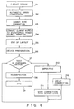
- Step S1 performs an IC design including a pattern as shown in Fig. 6.
- An automatic connection layout is performed at step S2 with the use of, for example, a layout CAD.
- a cell 5-1 for a power source connection only is included, but dummy wires 4 are not included.
- steps S3 dummy wires are provided at an unoccupied proper area on the connection layout.
- the dummy wire 4 is connected to an internal power source terminal line 2 at step S4.
- the automatic connection layout is completed at step S5.
- an actual device an integral circuit including the arrangement shown in Fig. 2 is prepared based on a resultant connection pattern layout at step S5.
- the device thus fabricated is tested for its state.
- Step S9 is terminated if it is determined at step S8 that the device is not defective. If, at a result of testing, the device is determined as being defective at step S10 and the defectiveness is found as being caused by a wrongly connected wire, connection correction is made at step S11 with the use of a dummy wire 4. If, on the other hand, the device is determined as being defective due to an incorrectness of a delay time in the integrated circuit involved, a connection correction is carried out, at step S12, with the use of the dummy wire 4. After the correction has been made at step S11 or S12, control goes back to step S7 to perform a test again. The correction operation is performed in a closed loop including steps S7 ⁇ S10 ⁇ S11 or S12 ⁇ S7 until no defectiveness is found at step S8.
- the dummy wire 4 is connected to the internal power source V SS terminal line which is opposite in potential to the substrate of the chip 20 as shown, for example, in Figs. 2 and 3.
- a capacitance C is created between the IC substrate 31 and the dummy wire 4 and connected to the internal power supply terminal 7. It is, therefore, possible to prevent a voltage fluctuation of the internal power source terminal and to supply a stable voltage to an internal circuit.
- the dummy wires 4 are formed at the same rate and width as those at which cell-to-cell wires 8 are arranged, making it possible to effect a connection correction as well as a delay time correction. For connection correction, as shown in Fig.
- the dummy wire 4-1 connected to the internal power source terminal 7 is electrically cut off the internal power source terminal 7. It is, therefore, possible to readily make the aforementioned correction operations in a short period of time. Those dummy wires left unused for correction are connected to the internal power source V SS terminal, serving to stabilize a power source potential.
- delay time correction as shown in Fig. 5, it is necessary in the prior art to newly add a cell or cells to an associated device, to restart a layout design and to prepare mask formation data all over again. According to the present invention, however, it is only necessary to provide the dummy wire 4-2, contact hole 3-2 and additional wire 22 as set out above.
- a wire density in the same connection layer can be made more uniform than that at which cell-to-cell wires alone are provided at that connection layer, reducing an extent of step (unevenness) on the surface of the integrated circuit resulting from a difference in wire density.
- the presence of the dummy wires 4 thus arranged ensures a uniform wire density against a "loading effect" which is produced in the case where, if a single wire alone, for example, is provided in a broader connection area, it is broken apart due to a corrosion developed at an etching step.
- a broken line 41 represents a layer surface state of an integrated circuit in which no dummy wires 4 are provided and a solid line 42 represents a layer surface state of the integrated circuit in which dummy wires are connected. From Fig. 3 it will be seen that the surface 42 of the integrated circuit is less stepped than the surface 41 of the integrated circuit.
- the present invention is not restricted to the aforementioned embodiment only. Various changes and modifications of the present invention can be made without departing from the scope of the present invention.
- an automatic array connection system such as a gate array system utilizing a basic cell.
- the wire is connected to a proper connection line or layer by the etch-back of the insulating film 32, the cutting of the connection line by a laser beam, formation of a contact hole, formation of an additional connection line (12, 22) by an aluminum evaporation method, etc.
Claims (2)
- Integrierte Halbleiterschaltungsanordnung, umfassend:wobei die mit dem zweiten Energiequellenpotential verbundenen Dummy-Verdrahtungen Mittel vorsehen zum Stabilisieren des zweiten Energiequellenpotentials und die Gesamtform der Anordnung der Vielzahl von Dummy-Verdrahtungen in Übereinstimmung ist mit der Form des Raumabschnitts, der von den Zwischenzellenverdrahtungen definiert ist.einen integrierten Halbleiterschaltungs-Chip (20) einschließlich eines Halbleitersubstrats (31), an das ein erstes Energiequellenpotential (VDD) angelegt ist;mindestens zwei Zellen-Arrays (5), von denen sich jedes in Longitudinalrichtung erstreckt und jedes eine Vielzahl von Zellen hat, die an einer Hauptfläche des Halbleitersubstrats angeordnet sind;eine Vielzahl von Zwischenzellenverdrahtungen (8) in einer Region zwischen den mindestens zwei Zellen-Arrays, wobei sich die Zwischenzellenverdrahtungen in der Longitudinalrichtung erstrecken;eine Vielzahl von Dummy-Verdrahtungen (4) in einem Raumabschnitt der Region zwischen den mindestens zwei Zellen-Arrays, der definiert ist in der Region zwischen den mindestens zwei Zellen-Arrays durch die Zwischenzellenverdrahtungen, wobei Verdrahtungen der Vielzahl von Dummy-Verdrahtungen verbunden sind mit einem inneren Energiequellenanschluss (7) mit einem zweiten Energiequellenpotential (VSS), das sich von dem ersten Energiequellenpotential unterscheidet;einer Isolationsschicht (32), die zwischen den Dummy-Verdrahtungen (4) und dem Substrat (31) derart vorgesehen ist, dass eine Kapazität (C) gebildet wird von den mit dem zweiten Energiequellenpotential verbundenen Dummy-Verdrahtungen (4), dem Substrat (31) und ihrer umgebenden Isolationsschicht (32); undeine Verbindungsschicht (2), die mit dem zweiten Energiepotential und den Dummy-Verdrahtungen über ein Kontaktloch (3) verbunden ist, wobei die Verbindungsschicht quer zu den Dummy-Verdrahtungen ist;
- Halbleiterschaltungsanordnung nach Anspruch 1, dadurch gekennzeichnet, dass die Dummy-Verdrahtungen (4) und der zweite Energiequellenanschluss (7) durch Drähte in einer spezifischen Zelle (5-1) verbunden sind, die für diesen Zweck bestimmt ist und wobei die spezifische Zelle in das Zellen-Array (5-2) der integrierten Halbleiterschaltung inkorporiert ist.
Applications Claiming Priority (3)
| Application Number | Priority Date | Filing Date | Title |
|---|---|---|---|
| JP1189312A JP2507618B2 (ja) | 1989-07-21 | 1989-07-21 | 半導体集積回路装置の製造方法 |
| JP189312/89 | 1989-07-21 | ||
| JP18931289 | 1989-07-21 |
Publications (3)
| Publication Number | Publication Date |
|---|---|
| EP0409256A2 EP0409256A2 (de) | 1991-01-23 |
| EP0409256A3 EP0409256A3 (en) | 1992-10-14 |
| EP0409256B1 true EP0409256B1 (de) | 2003-10-15 |
Family
ID=16239245
Family Applications (1)
| Application Number | Title | Priority Date | Filing Date |
|---|---|---|---|
| EP90113945A Expired - Lifetime EP0409256B1 (de) | 1989-07-21 | 1990-07-20 | Halbleiter-IC-Vorrichtung und deren Herstellungsverfahren |
Country Status (5)
| Country | Link |
|---|---|
| US (1) | US5160995A (de) |
| EP (1) | EP0409256B1 (de) |
| JP (1) | JP2507618B2 (de) |
| KR (1) | KR930009023B1 (de) |
| DE (1) | DE69034109T2 (de) |
Families Citing this family (14)
| Publication number | Priority date | Publication date | Assignee | Title |
|---|---|---|---|---|
| US5396100A (en) * | 1991-04-05 | 1995-03-07 | Hitachi, Ltd. | Semiconductor integrated circuit device having a compact arrangement of SRAM cells |
| JPH0851159A (ja) * | 1994-08-05 | 1996-02-20 | Mitsubishi Electric Corp | 半導体集積回路 |
| JP3180612B2 (ja) * | 1995-03-27 | 2001-06-25 | ヤマハ株式会社 | 半導体集積回路 |
| US5814847A (en) * | 1996-02-02 | 1998-09-29 | National Semiconductor Corp. | General purpose assembly programmable multi-chip package substrate |
| JP3159108B2 (ja) * | 1997-03-27 | 2001-04-23 | ヤマハ株式会社 | 半導体装置とその製造方法 |
| US5917230A (en) * | 1997-04-09 | 1999-06-29 | United Memories, Inc. | Filter capacitor construction |
| DE19825607C2 (de) * | 1998-06-08 | 2000-08-10 | Siemens Ag | Integrierte Halbleiterschaltung mit Füllstrukturen |
| JP4598470B2 (ja) * | 1998-07-03 | 2010-12-15 | パナソニック株式会社 | 半導体装置 |
| US6346427B1 (en) | 1999-08-18 | 2002-02-12 | Utmc Microelectronic Systems Inc. | Parameter adjustment in a MOS integrated circuit |
| US6323113B1 (en) * | 1999-12-10 | 2001-11-27 | Philips Electronics North America Corporation | Intelligent gate-level fill methods for reducing global pattern density effects |
| WO2005117115A1 (en) * | 2004-05-28 | 2005-12-08 | Koninklijke Philips Electronics N.V. | Chips with useful lines and dummy lines |
| JP4364226B2 (ja) * | 2006-09-21 | 2009-11-11 | 株式会社東芝 | 半導体集積回路 |
| US11239154B2 (en) * | 2015-01-20 | 2022-02-01 | Taiwan Semiconductor Manufacturing Company Ltd. | Fishbone structure enhancing spacing with adjacent conductive line in power network |
| US10523188B2 (en) | 2016-02-23 | 2019-12-31 | Samsung Electronics Co., Ltd. | Semiconductor device |
Family Cites Families (11)
| Publication number | Priority date | Publication date | Assignee | Title |
|---|---|---|---|---|
| JPS5852346B2 (ja) * | 1977-02-18 | 1983-11-22 | 株式会社東芝 | 半導体装置 |
| JPS59198796A (ja) * | 1983-04-26 | 1984-11-10 | 日本電気株式会社 | 高密度多層配線基板 |
| JPS60119749A (ja) * | 1983-12-02 | 1985-06-27 | Hitachi Ltd | 多層配線部材 |
| JPH0658947B2 (ja) * | 1984-02-24 | 1994-08-03 | 株式会社日立製作所 | 半導体メモリ装置の製法 |
| JPS61125045A (ja) * | 1984-11-22 | 1986-06-12 | Hitachi Ltd | 半導体装置 |
| JPS6218732A (ja) * | 1985-07-15 | 1987-01-27 | インタ−ナショナル ビジネス マシ−ンズ コ−ポレ−ション | 集積回路とその個性化方法 |
| JPS62206855A (ja) * | 1986-03-06 | 1987-09-11 | Nec Corp | 半導体装置の配線構造 |
| JPS6387744A (ja) * | 1986-09-30 | 1988-04-19 | Nec Corp | 半導体集積回路 |
| JPS63304496A (ja) * | 1987-06-03 | 1988-12-12 | Mitsubishi Electric Corp | 半導体記憶装置 |
| US4916514A (en) * | 1988-05-31 | 1990-04-10 | Unisys Corporation | Integrated circuit employing dummy conductors for planarity |
| JPH021928A (ja) * | 1988-06-10 | 1990-01-08 | Toshiba Corp | 半導体集積回路 |
-
1989
- 1989-07-21 JP JP1189312A patent/JP2507618B2/ja not_active Expired - Lifetime
-
1990
- 1990-07-20 EP EP90113945A patent/EP0409256B1/de not_active Expired - Lifetime
- 1990-07-20 DE DE69034109T patent/DE69034109T2/de not_active Expired - Lifetime
- 1990-07-21 KR KR1019900011110A patent/KR930009023B1/ko not_active IP Right Cessation
-
1991
- 1991-07-25 US US07/737,605 patent/US5160995A/en not_active Expired - Lifetime
Also Published As
| Publication number | Publication date |
|---|---|
| JP2507618B2 (ja) | 1996-06-12 |
| EP0409256A3 (en) | 1992-10-14 |
| KR910003801A (ko) | 1991-02-28 |
| DE69034109D1 (de) | 2003-11-20 |
| EP0409256A2 (de) | 1991-01-23 |
| KR930009023B1 (ko) | 1993-09-18 |
| US5160995A (en) | 1992-11-03 |
| DE69034109T2 (de) | 2004-07-29 |
| JPH0353547A (ja) | 1991-03-07 |
Similar Documents
| Publication | Publication Date | Title |
|---|---|---|
| EP0070861B1 (de) | Integrierte halbleiterscheibe sowie methode zur prüfung von auf dieser scheibe enthaltenen schaltungen | |
| EP0409256B1 (de) | Halbleiter-IC-Vorrichtung und deren Herstellungsverfahren | |
| US4467400A (en) | Wafer scale integrated circuit | |
| US4486705A (en) | Method of testing networks on a wafer having grounding points on its periphery | |
| EP0109006B1 (de) | Dynamischer Speicher mit wahlfreiem Zugriff mit getrennter Spannungsanschlussbahn zum "Verbrennen" und Verfahren zu dessen Herstellung und Prüfung | |
| KR20010007252A (ko) | 리페어용 퓨즈를 구비한 반도체 장치 및 퓨즈의 레이저트리밍 방법 | |
| EP0074825B1 (de) | Herstellung von integrierten Schaltungen nach dem Mutterscheibenverfahren | |
| US6591406B2 (en) | Semiconductor apparatus including bypass capacitor having structure for making automatic design easy, and semiconductor apparatus layout method | |
| US7442626B2 (en) | Rectangular contact used as a low voltage fuse element | |
| US6307162B1 (en) | Integrated circuit wiring | |
| KR19980026622A (ko) | 반도체 메모리셀의 레이아웃 | |
| EP0182222B1 (de) | Integrierte Halbleiterschaltungsanordnung in Polycell-Technik | |
| US3760384A (en) | Fet memory chip including fet devices therefor and fabrication method | |
| US6218721B1 (en) | Semiconductor device and method of manufacturing the same | |
| US7122434B2 (en) | Method for generating an electrical contact with buried track conductors | |
| US5952684A (en) | Chip layout of semiconductor integrated circuit | |
| EP0021661A1 (de) | Masterslice-Halbleitervorrichtung | |
| EP0069762B1 (de) | Ein universelles substrat zur wechselseitigen elektrischen verbindung von chips | |
| KR100413148B1 (ko) | 다층 구조물 내에 매립된 동일 평면 프로그램가능 퓨즈 | |
| US6236228B1 (en) | Structure and method of repair of integrated circuits | |
| US6730989B1 (en) | Semiconductor package and method | |
| US7060529B2 (en) | Multiple chip semiconductor arrangement having electrical components in separating regions | |
| JPS63301544A (ja) | スタンダ−ドセル方式の半導体集積回路 | |
| GB1306189A (de) | ||
| US6369406B1 (en) | Method for localizing point defects causing leakage currents in a non-volatile memory device |
Legal Events
| Date | Code | Title | Description |
|---|---|---|---|
| PUAI | Public reference made under article 153(3) epc to a published international application that has entered the european phase |
Free format text: ORIGINAL CODE: 0009012 |
|
| 17P | Request for examination filed |
Effective date: 19900720 |
|
| AK | Designated contracting states |
Kind code of ref document: A2 Designated state(s): DE FR GB |
|
| PUAL | Search report despatched |
Free format text: ORIGINAL CODE: 0009013 |
|
| AK | Designated contracting states |
Kind code of ref document: A3 Designated state(s): DE FR GB |
|
| 17Q | First examination report despatched |
Effective date: 19940725 |
|
| APAB | Appeal dossier modified |
Free format text: ORIGINAL CODE: EPIDOS NOAPE |
|
| APAB | Appeal dossier modified |
Free format text: ORIGINAL CODE: EPIDOS NOAPE |
|
| APAD | Appeal reference recorded |
Free format text: ORIGINAL CODE: EPIDOS REFNE |
|
| APAD | Appeal reference recorded |
Free format text: ORIGINAL CODE: EPIDOS REFNE |
|
| APCB | Communication from the board of appeal sent |
Free format text: ORIGINAL CODE: EPIDOS OBAPE |
|
| APCB | Communication from the board of appeal sent |
Free format text: ORIGINAL CODE: EPIDOS OBAPE |
|
| APAB | Appeal dossier modified |
Free format text: ORIGINAL CODE: EPIDOS NOAPE |
|
| GRAG | Despatch of communication of intention to grant |
Free format text: ORIGINAL CODE: EPIDOS AGRA |
|
| GRAH | Despatch of communication of intention to grant a patent |
Free format text: ORIGINAL CODE: EPIDOS IGRA |
|
| GRAH | Despatch of communication of intention to grant a patent |
Free format text: ORIGINAL CODE: EPIDOS IGRA |
|
| GRAA | (expected) grant |
Free format text: ORIGINAL CODE: 0009210 |
|
| AK | Designated contracting states |
Kind code of ref document: B1 Designated state(s): DE FR GB |
|
| REG | Reference to a national code |
Ref country code: GB Ref legal event code: FG4D |
|
| REF | Corresponds to: |
Ref document number: 69034109 Country of ref document: DE Date of ref document: 20031120 Kind code of ref document: P |
|
| ET | Fr: translation filed | ||
| PLBE | No opposition filed within time limit |
Free format text: ORIGINAL CODE: 0009261 |
|
| STAA | Information on the status of an ep patent application or granted ep patent |
Free format text: STATUS: NO OPPOSITION FILED WITHIN TIME LIMIT |
|
| 26N | No opposition filed |
Effective date: 20040716 |
|
| APAH | Appeal reference modified |
Free format text: ORIGINAL CODE: EPIDOSCREFNO |
|
| PGFP | Annual fee paid to national office [announced via postgrant information from national office to epo] |
Ref country code: FR Payment date: 20090710 Year of fee payment: 20 |
|
| PGFP | Annual fee paid to national office [announced via postgrant information from national office to epo] |
Ref country code: GB Payment date: 20090715 Year of fee payment: 20 Ref country code: DE Payment date: 20090716 Year of fee payment: 20 |
|
| REG | Reference to a national code |
Ref country code: GB Ref legal event code: PE20 Expiry date: 20100719 |
|
| PG25 | Lapsed in a contracting state [announced via postgrant information from national office to epo] |
Ref country code: GB Free format text: LAPSE BECAUSE OF EXPIRATION OF PROTECTION Effective date: 20100719 |
|
| PG25 | Lapsed in a contracting state [announced via postgrant information from national office to epo] |
Ref country code: DE Free format text: LAPSE BECAUSE OF EXPIRATION OF PROTECTION Effective date: 20100720 |