EP0375233A2 - Anzeigevorrichtung mit aktiver Matrix - Google Patents
Anzeigevorrichtung mit aktiver Matrix Download PDFInfo
- Publication number
- EP0375233A2 EP0375233A2 EP89312881A EP89312881A EP0375233A2 EP 0375233 A2 EP0375233 A2 EP 0375233A2 EP 89312881 A EP89312881 A EP 89312881A EP 89312881 A EP89312881 A EP 89312881A EP 0375233 A2 EP0375233 A2 EP 0375233A2
- Authority
- EP
- European Patent Office
- Prior art keywords
- pixel
- thin film
- pixel electrode
- storage capacitors
- display device
- Prior art date
- Legal status (The legal status is an assumption and is not a legal conclusion. Google has not performed a legal analysis and makes no representation as to the accuracy of the status listed.)
- Granted
Links
- 239000011159 matrix material Substances 0.000 title claims abstract description 10
- 239000003990 capacitor Substances 0.000 claims abstract description 71
- 230000002950 deficient Effects 0.000 claims abstract description 52
- 239000010409 thin film Substances 0.000 claims abstract description 25
- 230000007547 defect Effects 0.000 claims abstract description 23
- 238000000034 method Methods 0.000 claims description 10
- 239000000382 optic material Substances 0.000 claims description 10
- 239000000758 substrate Substances 0.000 claims description 10
- 230000000875 corresponding effect Effects 0.000 claims 3
- 239000010408 film Substances 0.000 description 26
- 239000004065 semiconductor Substances 0.000 description 17
- 239000004973 liquid crystal related substance Substances 0.000 description 9
- 238000010586 diagram Methods 0.000 description 7
- 239000012535 impurity Substances 0.000 description 6
- 239000000463 material Substances 0.000 description 6
- 210000002858 crystal cell Anatomy 0.000 description 5
- 238000009966 trimming Methods 0.000 description 4
- 239000000523 sample Substances 0.000 description 3
- 230000005540 biological transmission Effects 0.000 description 2
- 210000004027 cell Anatomy 0.000 description 2
- 238000005530 etching Methods 0.000 description 2
- 239000010410 layer Substances 0.000 description 2
- 238000003909 pattern recognition Methods 0.000 description 2
- 238000009877 rendering Methods 0.000 description 2
- 239000004020 conductor Substances 0.000 description 1
- 239000011229 interlayer Substances 0.000 description 1
- 238000005468 ion implantation Methods 0.000 description 1
- 239000007769 metal material Substances 0.000 description 1
- 229910021420 polycrystalline silicon Inorganic materials 0.000 description 1
- 239000010453 quartz Substances 0.000 description 1
- VYPSYNLAJGMNEJ-UHFFFAOYSA-N silicon dioxide Inorganic materials O=[Si]=O VYPSYNLAJGMNEJ-UHFFFAOYSA-N 0.000 description 1
- 238000011179 visual inspection Methods 0.000 description 1
Images


Classifications
-
- G—PHYSICS
- G02—OPTICS
- G02F—OPTICAL DEVICES OR ARRANGEMENTS FOR THE CONTROL OF LIGHT BY MODIFICATION OF THE OPTICAL PROPERTIES OF THE MEDIA OF THE ELEMENTS INVOLVED THEREIN; NON-LINEAR OPTICS; FREQUENCY-CHANGING OF LIGHT; OPTICAL LOGIC ELEMENTS; OPTICAL ANALOGUE/DIGITAL CONVERTERS
- G02F1/00—Devices or arrangements for the control of the intensity, colour, phase, polarisation or direction of light arriving from an independent light source, e.g. switching, gating or modulating; Non-linear optics
- G02F1/01—Devices or arrangements for the control of the intensity, colour, phase, polarisation or direction of light arriving from an independent light source, e.g. switching, gating or modulating; Non-linear optics for the control of the intensity, phase, polarisation or colour
- G02F1/13—Devices or arrangements for the control of the intensity, colour, phase, polarisation or direction of light arriving from an independent light source, e.g. switching, gating or modulating; Non-linear optics for the control of the intensity, phase, polarisation or colour based on liquid crystals, e.g. single liquid crystal display cells
- G02F1/133—Constructional arrangements; Operation of liquid crystal cells; Circuit arrangements
- G02F1/136—Liquid crystal cells structurally associated with a semi-conducting layer or substrate, e.g. cells forming part of an integrated circuit
- G02F1/1362—Active matrix addressed cells
- G02F1/13624—Active matrix addressed cells having more than one switching element per pixel
-
- G—PHYSICS
- G02—OPTICS
- G02F—OPTICAL DEVICES OR ARRANGEMENTS FOR THE CONTROL OF LIGHT BY MODIFICATION OF THE OPTICAL PROPERTIES OF THE MEDIA OF THE ELEMENTS INVOLVED THEREIN; NON-LINEAR OPTICS; FREQUENCY-CHANGING OF LIGHT; OPTICAL LOGIC ELEMENTS; OPTICAL ANALOGUE/DIGITAL CONVERTERS
- G02F1/00—Devices or arrangements for the control of the intensity, colour, phase, polarisation or direction of light arriving from an independent light source, e.g. switching, gating or modulating; Non-linear optics
- G02F1/01—Devices or arrangements for the control of the intensity, colour, phase, polarisation or direction of light arriving from an independent light source, e.g. switching, gating or modulating; Non-linear optics for the control of the intensity, phase, polarisation or colour
- G02F1/13—Devices or arrangements for the control of the intensity, colour, phase, polarisation or direction of light arriving from an independent light source, e.g. switching, gating or modulating; Non-linear optics for the control of the intensity, phase, polarisation or colour based on liquid crystals, e.g. single liquid crystal display cells
- G02F1/133—Constructional arrangements; Operation of liquid crystal cells; Circuit arrangements
- G02F1/136—Liquid crystal cells structurally associated with a semi-conducting layer or substrate, e.g. cells forming part of an integrated circuit
- G02F1/1362—Active matrix addressed cells
- G02F1/136213—Storage capacitors associated with the pixel electrode
-
- H—ELECTRICITY
- H01—ELECTRIC ELEMENTS
- H01L—SEMICONDUCTOR DEVICES NOT COVERED BY CLASS H10
- H01L27/00—Devices consisting of a plurality of semiconductor or other solid-state components formed in or on a common substrate
- H01L27/02—Devices consisting of a plurality of semiconductor or other solid-state components formed in or on a common substrate including semiconductor components specially adapted for rectifying, oscillating, amplifying or switching and having potential barriers; including integrated passive circuit elements having potential barriers
- H01L27/12—Devices consisting of a plurality of semiconductor or other solid-state components formed in or on a common substrate including semiconductor components specially adapted for rectifying, oscillating, amplifying or switching and having potential barriers; including integrated passive circuit elements having potential barriers the substrate being other than a semiconductor body, e.g. an insulating body
- H01L27/1214—Devices consisting of a plurality of semiconductor or other solid-state components formed in or on a common substrate including semiconductor components specially adapted for rectifying, oscillating, amplifying or switching and having potential barriers; including integrated passive circuit elements having potential barriers the substrate being other than a semiconductor body, e.g. an insulating body comprising a plurality of TFTs formed on a non-semiconducting substrate, e.g. driving circuits for AMLCDs
- H01L27/1255—Devices consisting of a plurality of semiconductor or other solid-state components formed in or on a common substrate including semiconductor components specially adapted for rectifying, oscillating, amplifying or switching and having potential barriers; including integrated passive circuit elements having potential barriers the substrate being other than a semiconductor body, e.g. an insulating body comprising a plurality of TFTs formed on a non-semiconducting substrate, e.g. driving circuits for AMLCDs integrated with passive devices, e.g. auxiliary capacitors
-
- G—PHYSICS
- G02—OPTICS
- G02F—OPTICAL DEVICES OR ARRANGEMENTS FOR THE CONTROL OF LIGHT BY MODIFICATION OF THE OPTICAL PROPERTIES OF THE MEDIA OF THE ELEMENTS INVOLVED THEREIN; NON-LINEAR OPTICS; FREQUENCY-CHANGING OF LIGHT; OPTICAL LOGIC ELEMENTS; OPTICAL ANALOGUE/DIGITAL CONVERTERS
- G02F1/00—Devices or arrangements for the control of the intensity, colour, phase, polarisation or direction of light arriving from an independent light source, e.g. switching, gating or modulating; Non-linear optics
- G02F1/01—Devices or arrangements for the control of the intensity, colour, phase, polarisation or direction of light arriving from an independent light source, e.g. switching, gating or modulating; Non-linear optics for the control of the intensity, phase, polarisation or colour
- G02F1/13—Devices or arrangements for the control of the intensity, colour, phase, polarisation or direction of light arriving from an independent light source, e.g. switching, gating or modulating; Non-linear optics for the control of the intensity, phase, polarisation or colour based on liquid crystals, e.g. single liquid crystal display cells
- G02F1/133—Constructional arrangements; Operation of liquid crystal cells; Circuit arrangements
- G02F1/136—Liquid crystal cells structurally associated with a semi-conducting layer or substrate, e.g. cells forming part of an integrated circuit
- G02F1/1362—Active matrix addressed cells
- G02F1/136259—Repairing; Defects
- G02F1/136268—Switch defects
Definitions
- the present invention relates to an active matrix type display device.
- FIG. 2 is a circuit diagram showing one example of a liquid crystal display device employing thin film transistors (hereinafter abbreviated as "TFTs").
- TFTs thin film transistors
- two TFTs 11 and 12 are disposed at the inter-section between a signal line Xn and a scanning line Yn, and an image signal is written in a liquid crystal cell 20.
- V0 does not equal V1
- V1 the voltage that is applied to the pixel in the two cases, that is when the pixel is driven by a single TFT and when it is driven by two TFTs, differs. A marked difference in the transmission factor thus occurs particularly in a half tone display. Accordingly, the pixel defect cannot be relieved even by the use of redundancy.
- the present invention provides an active matrix type display device having a plurality of scanning lines, a plurality of signal lines, and pixels disposed at inter-sections of the scanning lines and the signal lines for providing a display, each pixel being driven by way of a respective plurality of thin film transistors which are connected to an associated pixel electrode, characterised in that each pixel electrode has connected thereto a respective plurality of storage capacitors arranged in parallel.
- a defect in a pixel caused either by a thin film transistor or by a storage capacitor connected to one of the pixel electrodes being defective, can be relieved simply by electrically disconnecting the defective portion. If a defective thin film transistor and an associated storage capacitor are simultaneously disconnected as a pair and the magnitude of the capacitance removed is optimised, it is possible still to apply to the relevant pixel the same signal as is applied to the normal pixels. In other words, the pixel defect can be completely relieved.
- FIG. 1 shows a display device employing redundancy and having a liquid crystal material as an electro-optic material and two TFTs 1 and 2 for driving each pixel.
- These two TFTs 1 and 2 have their respective source electrodes connected to a common signal line Xm, their respective gate electrodes connected to a common scanning line Yn and their respective drain electrodes connected to a point P, that is to a common pixel electrode. Therefore, the two TFTs 1 and 2 are electrically equivalent to each other.
- the pixel electrode P is connected to a liquid crystal cell 10, and to storage capacitors 5 and 6, respectively.
- both the two TFTs 1 and 2 have satisfactory writing capability.
- a pixel defect is detected and relieved as follows. First, the address of a defective TFT is obtained either electrically or optically. The following are specific examples of methods for detecting a defective TFT in the substrate:
- a method wherein the address of a defective TFT is obtained from the image pattern displayed may be employed. For example, if there is a short between the gate and source of a TFT or between the gate and drain, the scanning line select pulse appears on the signal line. Therefore, the address of the defective TFT can be obtained from the timing at which the select pulse appears. If there is a short between the source and drain of a TFT, an image signal is applied to the pixel electrode from the signal line when all the scanning lines are placed in a non-select state. Therefore, the address of the defective TFT is readily obtained from the image pattern displayed. Since the two TFTs for driving each pixel are electrically equivalent to each other, if the address of a defective TFT is obtained by a method other than pattern recognition, the defective one of the TFTs may be determined by visual inspection.
- the TFT that is considered to be defective is disconnected or cut off by the use of laser trimming or other similar means, and the storage capacitor 5 of the pixel concerned is also disconnected or cut off.
- the potential at the pixel electrode P alters by an amount determined by the gate-drain capacitances C3, C4 of the TFTs 1 and 2, the capacitances C5, C6 of the storage capacitors 5 and 6, and the liquid crystal capacitance C0.
- the capacitance of the electro-optic material of the pixel is C0
- the total capacitance of the storage capacitors for each pixel is Cs
- the gate-drain capacitance of the i-th TFT is ci
- the gate-drain capacitance of the remaining N-1 TFTs is Cn-1.
- the same voltage may be applied to the pixel as in the case where the pixel is driven by the N TFTs.
- FIG. 3 is a circuit diagram showing another embodiment of the present invention.
- storage capacitors are interposed between the pixel electrode P and the scanning line Yn-1 in the preceding stage, but the basic operation is the same as in the case of the embodiment shown in Figure 1. It is assumed that the magnitudes of the gate-drain capacitances 23 and 24 of two TFTs 21 and 22 are C3 and C4, respectively, the capacitances of three storage capacitors 25, 26 and 27 are C5, C6 and C7, respecively, and the capacitance of a liquid crystal cell 30 is C0.
- the operation of the pixel can be corrected regardless of whether a TFT or a storage capacitor is defective. It is impossible, however, to correct the pixel in the following two cases, that is, when the two TFTs 21 and 22 are simultaneously defective, or when the three storage capacitors are simultaneously defective. Nevertheless, the probability that such a case will occur is extremely low. Therefore, it is possible to correct most pixel defects.
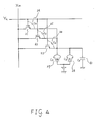
- FIG 4 is a circuit diagram showing still another embodiment of the present invention.
- MOS capacitors are employed as two storage capacitors 37 and 38, respectively, but the basic operation is the same as in the case of the embodiment shown in Figure 1. It is assumed that the magnitudes of the gate-drain capacitances 34, 35 and 36 of three TFTs 31, 32 and 33 are C4, C5 and C6, respectively, the capacitances of the two storage capacitors 37 and 38 are C7 and C8, respectively, and the capacitance of a liquid crystal cell 40 is C0.
- FIG. 5 is a circuit diagram showing a further embodiment of the present invention.
- This embodiment features a redundancy arrangement wherein two TFTs 41 and 42 and two signal lines are disposed for driving each pixel. These two TFTs have their own respective gate electrodes connected to a common scanning line Yn and their respective drain electrodes connected to a common pixel electrode P. However, the source electrodes of the two TFTs are connected to signal lines X2m-1 and X2m, respectively.
- the capacitance of an electro-optic cell 50 is C0
- the capacitances of storage capacitors 45, 46 and 47 are C5, C6 and C7, respectively
- the magnitudes of the gate-drain capacitances 43 and 44 of the two TFTs 41 and 42 are C3 and C4, respectively.
- the first advantage resides in the fact that the address of a defective TFT can be obtained readily and accurately.
- the address of a defective TFT may be obtained electrically by the following two methods, that is by applying a probe directly to each pixel electrode or by applying proper signals to the signal and scanning lines to obtain indirectly the address of a defective TFT.
- the address of a defective TFT can also be obtained extremely easily optically by making a comparison between the image pattern that is displayed on a completed panel by the application of image signals to the odd signal lines alone and the image pattern that is displayed by the application of image signals to the even signal lines alone.
- the second advantage resides in the fact that it is possible to relieve a defect in a pixel resulting from a disconnection of a signal line or a short between the signal and scanning lines. If the respective terminals of the two signal lines X2m-1 and X2m are shorted to each other and the same signal is applied to them, the disconnection is automatically disregarded unless the signal line(s) is disconnected at two or more positions. If either of the signal lines X2m-1 or X2m and the scanning line Yn are shorted to each other, the signal line may be disconnected at both sides of the shorting portion, thus rendering the signal and scanning lines operative again.
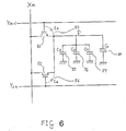
- FIG. 6 is a circuit diagram showing a still further embodiment of the present invention.
- This embodiment features a redundancy arrangement wherein two TFTs 51 and 52 and two scanning lines are provided for each pixel. These two TFTs have their respective source electrodes connected to a common signal line Xm and their respective drain electrodes connected to a common pixel electrode P. However, the gate electrodes of the two TFTs are connected to scanning lines Y2n-1 and Y2n, respectively.
- the capacitance of an electro-optic cell 60 is C0
- the capacitances of storage capacitors 55, 56 and 57 are C5, C6 and C7, respectively
- the magnitudes of the gate-drain capacitances 53 and 54 of two TFTs 51 and 52 are C3 and C4, respectively.
- the first advantage resides in the fact that the address of a defective TFT can be obtained readily and accurately.
- the address of a defective TFT may be obtain electrically by the following two methods, that is by applying a probe directly to each pixel electrode or by applying proper signals to the signal and scanning lines to obtain indirectly the address of a defective TFT.
- the address of a defective TFT can also be obtained extremely easily optically by making a comparison between the image pattern that is displayed on a completed panel by the application of scanning signals to the odd scanning lines alone and the image pattern that is displayed by the application of scanning signals to the even scanning lines alone.
- the second advantage resides in the fact that it is possible to relieve a defect in a pixel resulting from a disconnection of a signal line or a short between the signal and scanning lines. If the respective terminals of the two scanning lines Y2n-1 and Y2n are shorted to each other and the same signal is applied to them, the disconnection is automatically avoided unless the scanning line(s) is disconnected at two or more positions. If the signal line Xm and either of the scanning lines Y2n-1 or Y2n are shorted to each other, the scanning line may be disconnected at both sides of the shorting portion, thus rendering the signal and scanning lines operative again.
- FIG 7 is a top view of one pixel of the embodiment of a display device according to the present invention shown in Figure 1.
- the two TFTs provided for each pixel have their sources 103 connected to the signal line Xm, and their drains 104 connected to a pixel electrode 101.
- Their gates 102 are constituted by the scanning line Yn itself.
- the reference numeral 105 denotes channel regions made of a semi-conductor film.
- An insulating film is formed between the semi-conductor film 105 of the gates 102.
- Common electrodes 111 and 112 form respective storage capacitors between the same and the pixel electrode 101. The capacitances of the storage capacitors are assumed to be C5 and C6, respectively, as mentioned above.
- the pixel electrode 101 faces an opposing electrode through an electro-optic material to form a capacitance there-between.
- the magnitude of the capacitance is assumed to be C0. Since the respective sizes of the TFTs are equal to one another, the first equation holds. It is assumed that the second equation holds for C0, C5 and C6.
- the portions denoted by the reference numeral 113 are cut out by means of laser trimming or another similar technique and, at the same time, the portion denoted by the reference numeral 115 is cut out to disconnect the common electrode 111. If the right hand TFT is found to be defective, the portions 114 and 115 are similarly cut out. It is preferable for the line width of the cut out portions 113 and 114 to be smaller than the width of the channel region of each TFT and for the line width of the cut out portion 115 to be smaller than the width of the pixel electrode 101.
- Figure 8 is a cross sectional view taken along the line A - B in Figure 7.
- the common electrodes 111 and 112 are provided on an insulating substrate 110 below the pixel electrode 101 with an insulating film 109 interposed there-between so that no unnecessary voltage will be applied to the electro-optic material.
- a gate insulating film 107 and a semi-conductor film 106 are stacked over the gate 102, and the source 103 and the drain 104 are connected to the corresponding portions of the semi-conductor film 106.
- a transmission type display device is formed, whereas, if a semi-conductor substrate is employed in place of the insulating substrate 110 and a metallic material is employed to constitute pixel electrodes, a reflective type display device is formed.
- FIG. 9 is a top view of one pixel of another embodiment of the display device according to the present invention.
- the TFTs have their sources 123 connected to a signal line Xm, their drains 124 connected to a pixel electrode 121 and their gates 122 connected to a scanning line Yn.
- a semi-conductor film that is denoted by the reference numeral 125 constitutes channel regions for the TFTs.
- An etching stopper 128 is provided to make the film thickness of the channel regions uniform.
- Storage capacitor electrodes 131 and 132 face a scanning line Yn-1 in the preceding stage through an insulating film to form capacitances therebetween.
- the pixel electrode 121 faces an opposing electrode through an electro-optic material to constitute a capacitance.
- cuts are made at portions 133, 134 or 135, whereas, when a storage capacitor is to be disconnected, cuts are made at portions 136 or 137, using laser trimming or other similar means.
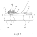
- Figure 10 is a cross sectional view taken along the line A - B in Figure 9.
- the storage capacitor electrode 131 is provided above a scanning line 139 in the preceding stage, with an insulating film 129 interposed there-between so that no unnecessary voltage will be applied to the electro-optic material and the display quality and the reliability of the device are enhanced.
- the insulating film 129 and the semi-conductor film 125 are stacked over the gate 122.
- the source 123 and the drain 124 are connected to the semi-conductor film 125 through a semi-conductor film 126 having a large amount of impurity implanted therein.
- the etching stopper 128 is disposed over the channel region provided by the semi-conductor film 125.
- the pixel electrode 121 which is formed of a transparent conductive film, is connected to both the drain 124 and the storage capacitor electrode 131.
- the insulating film 129 may comprise a multi-layer film so as to reduce pin holes.
- the MOS capacitor electrode 170 has a low impurity concentration, and if the semi-conductor material is of n-type, a positive voltage is applied to a common electrode 160, whereas, if the semi-conductor material is of p-type, a negative voltage is applied to the common electrode 160, to form an inversion layer on the surface of the semi-conductor material whereby the electrode 170 functions as a MOS capacitor.
- the impurity concentration of the MOS capacitor electrode 170 is high, the potential at the common electrode 160 can be set as desired. If the MOS capacitor and the TFTs have the same conductivity type, the MOS capacitor can be formed at the same time as the TFTs.
- the common electrode 160 is formed of the same film as that used to form the gate 142, while the MOS capacitor electrode 170 is formed of the same semi-conductor film as that used to form the source, drain and channel regions of the TFTs.
- the signal line 159 and the pixel electrode 141 are connected to the source and drain regions and the MOS capacitor electrode through the respective contact holes.
- An inter-layer insulating film 148 isolates the scanning and signal lines from each other. If quartz is used as an insulating substrate and polycrystalline silicon as a semi-conductor material, it is possible to employ a thermal oxide film to constitute the gate insulating film 149.
- the display device is capable of relieving completely a defect in a pixel regardless of whether a TFT or a storage capacitor associated with the pixel is defective. Accordingly, the product yield may be increased markedly, and it is possible to produce a defect free display device at a reduced cost.
- the uniformity of the picture is improved by a large margin, so that the size and density of the picture may readily be increased. Also, it is possible to provide strict gradation in a display of data including half tones, so that the range of application of the display device is enlarged.
- a DC voltage is applied to a defective pixel and this causes a reduction in the life of the electro-optic material.
- the present invention not only eliminates defects in pixels but also enables the same voltage to be applied both to a recovered pixel and to the normal pixels. Therefore, it is possible to realise a display device having a high reliability.
- the present invention thus provides a highly advantageous arrangement based on redundancy for providing relief for defects in pixels.
Landscapes
- Physics & Mathematics (AREA)
- Engineering & Computer Science (AREA)
- Nonlinear Science (AREA)
- Microelectronics & Electronic Packaging (AREA)
- Power Engineering (AREA)
- General Physics & Mathematics (AREA)
- Optics & Photonics (AREA)
- Crystallography & Structural Chemistry (AREA)
- Chemical & Material Sciences (AREA)
- Mathematical Physics (AREA)
- Condensed Matter Physics & Semiconductors (AREA)
- Computer Hardware Design (AREA)
- Liquid Crystal (AREA)
- Design And Manufacture Of Integrated Circuits (AREA)
- Thin Film Transistor (AREA)
- Liquid Crystal Display Device Control (AREA)
Applications Claiming Priority (2)
| Application Number | Priority Date | Filing Date | Title |
|---|---|---|---|
| JP321361/88 | 1988-12-20 | ||
| JP63321361A JPH02165125A (ja) | 1988-12-20 | 1988-12-20 | 表示装置 |
Publications (3)
| Publication Number | Publication Date |
|---|---|
| EP0375233A2 true EP0375233A2 (de) | 1990-06-27 |
| EP0375233A3 EP0375233A3 (de) | 1991-01-16 |
| EP0375233B1 EP0375233B1 (de) | 1994-05-18 |
Family
ID=18131714
Family Applications (1)
| Application Number | Title | Priority Date | Filing Date |
|---|---|---|---|
| EP89312881A Expired - Lifetime EP0375233B1 (de) | 1988-12-20 | 1989-12-11 | Anzeigevorrichtung mit aktiver Matrix |
Country Status (4)
| Country | Link |
|---|---|
| US (1) | US5173792A (de) |
| EP (1) | EP0375233B1 (de) |
| JP (1) | JPH02165125A (de) |
| DE (1) | DE68915413T2 (de) |
Cited By (10)
| Publication number | Priority date | Publication date | Assignee | Title |
|---|---|---|---|---|
| EP0438138A2 (de) * | 1990-01-17 | 1991-07-24 | Kabushiki Kaisha Toshiba | Flüssigkristall-Anzeigevorrichtung mit aktiver Matrix |
| EP0466377A2 (de) * | 1990-07-09 | 1992-01-15 | International Business Machines Corporation | Flüssigkristall-Anzeigevorrichtung zur Anzeige von Halbtonbildern |
| EP0488808A2 (de) * | 1990-11-30 | 1992-06-03 | Sharp Kabushiki Kaisha | Substrat mit aktiver Matrix |
| EP0490640A1 (de) * | 1990-12-10 | 1992-06-17 | Semiconductor Energy Laboratory Co., Ltd. | Elektronische Anordnungen, insbesondere für die Anwendung als elektro-optische Vorrichtungen |
| US5287206A (en) * | 1990-11-30 | 1994-02-15 | Sharp Kabushiki Kaisha | Active matrix display device |
| WO2002052336A2 (en) * | 2000-12-22 | 2002-07-04 | Electronics For Imaging, Inc. | Methods and apparatus for repairing inoperative pixels in a display |
| EP1239323A1 (de) * | 2001-02-27 | 2002-09-11 | Sharp Kabushiki Kaisha | Anzeigegerät mit Aktivmatrix |
| US6753839B2 (en) | 2000-12-14 | 2004-06-22 | Seiko Epson Corporation | Electro-optical panel and electronic device |
| EP2343593A1 (de) * | 2008-11-05 | 2011-07-13 | Sharp Kabushiki Kaisha | Aktivmatrixsubstrat, verfahren zur herstellung eines aktivmatrixsubstrats, flüssigkristallschirm, verfahren zum herstellen eines flüssigkristallschirms und flüssigkristallanzeigeanordnung, flüssigkristallanzeigeeinheit und fernsehempfänger |
| EP2357520A1 (de) * | 2008-12-10 | 2011-08-17 | Sharp Kabushiki Kaisha | Aktivmatrixsubstrat, verfahren zur herstellung eines aktivmatrixsubstrats, flüssigkristallschirm, verfahren zur herstellung eines flüssigkristallschirms, flüssigkristallanzeigeanordnung, flüssigkristallanzeigeeinheit und fernsehempfänger |
Families Citing this family (55)
| Publication number | Priority date | Publication date | Assignee | Title |
|---|---|---|---|---|
| JP2711015B2 (ja) * | 1990-07-25 | 1998-02-10 | 三菱電機株式会社 | マトリクス形表示装置 |
| US6713783B1 (en) * | 1991-03-15 | 2004-03-30 | Semiconductor Energy Laboratory Co., Ltd. | Compensating electro-optical device including thin film transistors |
| JPH07119919B2 (ja) * | 1991-05-15 | 1995-12-20 | インターナショナル・ビジネス・マシーンズ・コーポレイション | 液晶表示装置 |
| US5414278A (en) * | 1991-07-04 | 1995-05-09 | Mitsushibi Denki Kabushiki Kaisha | Active matrix liquid crystal display device |
| JPH05119344A (ja) * | 1991-10-25 | 1993-05-18 | Nec Corp | 液晶表示デバイス |
| GB9219836D0 (en) * | 1992-09-18 | 1992-10-28 | Philips Electronics Uk Ltd | Electronic drive circuits for active matrix devices,and a method of self-tasting and programming such circuits |
| KR100268007B1 (ko) * | 1992-12-22 | 2000-10-16 | 구본준 | 액정표시소자 제조방법 |
| US5555001A (en) * | 1994-03-08 | 1996-09-10 | Prime View Hk Limited | Redundant scheme for LCD display with integrated data driving circuit |
| JP3402400B2 (ja) | 1994-04-22 | 2003-05-06 | 株式会社半導体エネルギー研究所 | 半導体集積回路の作製方法 |
| US6747627B1 (en) | 1994-04-22 | 2004-06-08 | Semiconductor Energy Laboratory Co., Ltd. | Redundancy shift register circuit for driver circuit in active matrix type liquid crystal display device |
| CN1230919C (zh) * | 1994-06-02 | 2005-12-07 | 株式会社半导体能源研究所 | 有源矩阵显示器和电光元件 |
| JP3897826B2 (ja) * | 1994-08-19 | 2007-03-28 | 株式会社半導体エネルギー研究所 | アクティブマトリクス型の表示装置 |
| US5956008A (en) * | 1994-09-06 | 1999-09-21 | Semiconductor Energy Laboratory Co., | Driver circuit for active matrix display and method of operating same |
| US5929464A (en) * | 1995-01-20 | 1999-07-27 | Semiconductor Energy Laboratory Co., Ltd. | Active matrix electro-optical device |
| JP3418653B2 (ja) | 1995-09-28 | 2003-06-23 | シャープ株式会社 | アクティブマトリクス型液晶表示装置 |
| JP3256110B2 (ja) * | 1995-09-28 | 2002-02-12 | シャープ株式会社 | 液晶表示装置 |
| JP4059292B2 (ja) * | 1996-09-26 | 2008-03-12 | セイコーエプソン株式会社 | 表示装置 |
| GB9705417D0 (en) * | 1997-03-15 | 1997-04-30 | Sharp Kk | Fault tolerant circuit arrangements |
| KR100430773B1 (ko) * | 1998-07-14 | 2004-05-10 | 가부시끼가이샤 도시바 | 액티브 매트릭스형 액정표시장치 |
| US6512504B1 (en) | 1999-04-27 | 2003-01-28 | Semiconductor Energy Laborayory Co., Ltd. | Electronic device and electronic apparatus |
| JP4755748B2 (ja) * | 1999-09-24 | 2011-08-24 | 東芝モバイルディスプレイ株式会社 | 平面表示装置 |
| TWI301915B (de) | 2000-03-17 | 2008-10-11 | Seiko Epson Corp | |
| JP3645184B2 (ja) * | 2000-05-31 | 2005-05-11 | シャープ株式会社 | 液晶表示装置及びその欠陥修正方法 |
| JP4925528B2 (ja) * | 2000-09-29 | 2012-04-25 | 三洋電機株式会社 | 表示装置 |
| JP4632522B2 (ja) * | 2000-11-30 | 2011-02-16 | Nec液晶テクノロジー株式会社 | 反射型液晶表示装置の製造方法 |
| TW466673B (en) * | 2000-12-11 | 2001-12-01 | Unipac Optoelectronics Corp | Cst on common structure |
| GB0112561D0 (en) * | 2001-05-23 | 2001-07-18 | Koninl Philips Electronics Nv | Active plate |
| KR100469342B1 (ko) * | 2001-07-11 | 2005-02-02 | 엘지.필립스 엘시디 주식회사 | 액정표시소자 |
| US7112517B2 (en) | 2001-09-10 | 2006-09-26 | Semiconductor Energy Laboratory Co., Ltd. | Laser treatment device, laser treatment method, and semiconductor device fabrication method |
| JP2003091245A (ja) | 2001-09-18 | 2003-03-28 | Semiconductor Energy Lab Co Ltd | 表示装置 |
| US6862052B2 (en) * | 2001-12-14 | 2005-03-01 | Samsung Electronics Co., Ltd. | Liquid crystal display, thin film transistor array panel for liquid crystal display and manufacturing method thereof |
| US20040110326A1 (en) * | 2002-11-20 | 2004-06-10 | Charles Forbes | Active matrix thin film transistor array backplane |
| TWI224234B (en) * | 2003-08-12 | 2004-11-21 | Quanta Display Inc | Pixel structure and fabricating method thereof |
| KR20050041010A (ko) * | 2003-10-29 | 2005-05-04 | 삼성전자주식회사 | 박막 다이오드 표시판 및 그 제조 방법 |
| TWI277935B (en) * | 2004-01-06 | 2007-04-01 | Hannstar Display Corp | Pixel structure and exposure method thereof |
| JP4627081B2 (ja) * | 2004-01-28 | 2011-02-09 | シャープ株式会社 | アクティブマトリクス基板及び表示装置 |
| JP4088619B2 (ja) * | 2004-01-28 | 2008-05-21 | シャープ株式会社 | アクティブマトリクス基板及び表示装置 |
| JP2005252228A (ja) * | 2004-02-05 | 2005-09-15 | Sharp Corp | 表示装置及びその製造方法 |
| TWI282969B (en) * | 2004-04-29 | 2007-06-21 | Au Optronics Corp | Thin film transistor array and fabricating method thereof |
| US20050275352A1 (en) * | 2004-06-14 | 2005-12-15 | Au Optronics Corporation. | Redundant storage capacitor and method for repairing OLED pixels and driving circuits |
| JP4829534B2 (ja) * | 2005-05-31 | 2011-12-07 | シャープ株式会社 | 薄膜トランジスタマトリクス基板及びその欠陥修復方法 |
| CN100555366C (zh) * | 2005-09-22 | 2009-10-28 | 夏普株式会社 | 有源矩阵衬底、显示装置、电视接收装置、有源矩阵衬底的制造方法、以及显示装置的制造方法 |
| US8947297B2 (en) * | 2006-01-30 | 2015-02-03 | The Invention Science Fund I, Llc | Positional display elements |
| KR101232157B1 (ko) * | 2006-06-09 | 2013-02-12 | 엘지디스플레이 주식회사 | Lcd 검사 장비 |
| JP5004908B2 (ja) * | 2008-09-05 | 2012-08-22 | パナソニック液晶ディスプレイ株式会社 | 液晶表示装置 |
| EP2256544A1 (de) * | 2009-05-27 | 2010-12-01 | Polymer Vision Limited | Verfahren zur Herstellung einer Anzeigetafel und Anzeigetafel mit reparierfähigen Elementen |
| TWI409894B (zh) * | 2010-07-09 | 2013-09-21 | Chunghwa Picture Tubes Ltd | 薄膜電晶體之對位檢測方法 |
| CN103018987B (zh) * | 2012-12-06 | 2015-05-13 | 京东方科技集团股份有限公司 | 阵列基板及显示装置 |
| KR20140120167A (ko) * | 2013-04-02 | 2014-10-13 | 삼성디스플레이 주식회사 | 수리된 화소를 갖는 유기전계발광 표시장치 및 그의 화소 수리방법 |
| JP6402713B2 (ja) * | 2013-06-27 | 2018-10-10 | 凸版印刷株式会社 | 薄膜トランジスタアレイ、その製造方法、画像表示装置及び表示方法 |
| JP6451054B2 (ja) * | 2014-01-23 | 2019-01-16 | 凸版印刷株式会社 | 薄膜トランジスタアレイ、その製造方法及び画像表示装置 |
| KR102296945B1 (ko) * | 2014-07-04 | 2021-09-01 | 엘지디스플레이 주식회사 | 유기 발광 표시 장치 및 그 제조 방법 |
| CN109270756B (zh) | 2018-09-30 | 2020-12-25 | 惠科股份有限公司 | 一种显示面板和显示装置 |
| JP7193404B2 (ja) * | 2019-03-29 | 2022-12-20 | 株式会社ジャパンディスプレイ | 表示装置 |
| CN114446187B (zh) * | 2020-11-03 | 2023-06-27 | 成都辰显光电有限公司 | 驱动背板、显示面板及其制备方法 |
Citations (2)
| Publication number | Priority date | Publication date | Assignee | Title |
|---|---|---|---|---|
| US4431271A (en) * | 1979-09-06 | 1984-02-14 | Canon Kabushiki Kaisha | Display device with a thin film transistor and storage condenser |
| EP0112700A2 (de) * | 1982-12-25 | 1984-07-04 | Kabushiki Kaisha Toshiba | Dünnfilm-Transistorschaltung |
Family Cites Families (15)
| Publication number | Priority date | Publication date | Assignee | Title |
|---|---|---|---|---|
| US3532813A (en) * | 1967-09-25 | 1970-10-06 | Rca Corp | Display circuit including charging circuit and fast reset circuit |
| JPS55120175A (en) * | 1979-03-12 | 1980-09-16 | Clarion Co Ltd | Variable capacitance diode with plural super-capacitance variable electrode structures |
| US4748445A (en) * | 1983-07-13 | 1988-05-31 | Citizen Watch Co., Ltd. | Matrix display panel having a diode ring structure as a resistive element |
| US4639087A (en) * | 1984-08-08 | 1987-01-27 | Energy Conversion Devices, Inc. | Displays having pixels with two portions and capacitors |
| US4728172A (en) * | 1984-08-08 | 1988-03-01 | Energy Conversion Devices, Inc. | Subassemblies for displays having pixels with two portions and capacitors |
| GB8508656D0 (en) * | 1985-04-03 | 1985-05-09 | Gen Electric Co Plc | Liquid crystal displays |
| US4728175A (en) * | 1986-10-09 | 1988-03-01 | Ovonic Imaging Systems, Inc. | Liquid crystal display having pixels with auxiliary capacitance |
| US4820222A (en) * | 1986-12-31 | 1989-04-11 | Alphasil, Inc. | Method of manufacturing flat panel backplanes including improved testing and yields thereof and displays made thereby |
| US4762398A (en) * | 1987-01-26 | 1988-08-09 | Hosiden Electronics Co., Ltd. | Pixel transistor free of parasitic capacitance fluctuations from misalignment |
| DE3851557T2 (de) * | 1987-03-18 | 1995-01-26 | Matsushita Electric Ind Co Ltd | Videoprojektor. |
| GB2206721A (en) * | 1987-07-03 | 1989-01-11 | Philips Electronic Associated | Active matrix display device |
| JPS6437585A (en) * | 1987-08-04 | 1989-02-08 | Nippon Telegraph & Telephone | Active matrix type display device |
| JPS6473324A (en) * | 1987-09-14 | 1989-03-17 | Matsushita Electric Ind Co Ltd | Display device and its driving method |
| JPH0251129A (ja) * | 1988-08-12 | 1990-02-21 | Sanyo Electric Co Ltd | アクテイブマトリクス液晶表示パネル |
| KR940005124B1 (ko) * | 1989-10-04 | 1994-06-11 | 호시덴 가부시기가이샤 | 액정표시소자 |
-
1988
- 1988-12-20 JP JP63321361A patent/JPH02165125A/ja active Pending
-
1989
- 1989-12-11 EP EP89312881A patent/EP0375233B1/de not_active Expired - Lifetime
- 1989-12-11 DE DE68915413T patent/DE68915413T2/de not_active Expired - Lifetime
- 1989-12-19 US US07/454,396 patent/US5173792A/en not_active Expired - Lifetime
Patent Citations (2)
| Publication number | Priority date | Publication date | Assignee | Title |
|---|---|---|---|---|
| US4431271A (en) * | 1979-09-06 | 1984-02-14 | Canon Kabushiki Kaisha | Display device with a thin film transistor and storage condenser |
| EP0112700A2 (de) * | 1982-12-25 | 1984-07-04 | Kabushiki Kaisha Toshiba | Dünnfilm-Transistorschaltung |
Non-Patent Citations (1)
| Title |
|---|
| JAPAN DISPLAY'86, 1986, pages 208-211; H. OGURA et al.: "Active matrix color LCD fabricated by using redudancy and repair system" * |
Cited By (26)
| Publication number | Priority date | Publication date | Assignee | Title |
|---|---|---|---|---|
| EP0438138A3 (en) * | 1990-01-17 | 1992-04-29 | Kabushiki Kaisha Toshiba | Liquid-crystal display device of active matrix type |
| EP0438138A2 (de) * | 1990-01-17 | 1991-07-24 | Kabushiki Kaisha Toshiba | Flüssigkristall-Anzeigevorrichtung mit aktiver Matrix |
| EP0466377A3 (en) * | 1990-07-09 | 1992-09-02 | International Business Machines Corporation | Liquid crystal display for displaying half-tone images |
| EP0466377A2 (de) * | 1990-07-09 | 1992-01-15 | International Business Machines Corporation | Flüssigkristall-Anzeigevorrichtung zur Anzeige von Halbtonbildern |
| EP0488808A3 (en) * | 1990-11-30 | 1992-11-04 | Sharp Kabushiki Kaisha | An active matrix substrate |
| US5276540A (en) * | 1990-11-30 | 1994-01-04 | Sharp Kabushiki Kaisha | Active matrix substrate with conductive film covering transparent conductive film portion connecting additional and non-additional capacitance portions of pixel electrode |
| US5287206A (en) * | 1990-11-30 | 1994-02-15 | Sharp Kabushiki Kaisha | Active matrix display device |
| EP0488808A2 (de) * | 1990-11-30 | 1992-06-03 | Sharp Kabushiki Kaisha | Substrat mit aktiver Matrix |
| EP0490640A1 (de) * | 1990-12-10 | 1992-06-17 | Semiconductor Energy Laboratory Co., Ltd. | Elektronische Anordnungen, insbesondere für die Anwendung als elektro-optische Vorrichtungen |
| US5165075A (en) * | 1990-12-10 | 1992-11-17 | Semiconductor Energy Laboratory Co., Ltd. | Electro-optic device having pairs of complementary transistors |
| US5572047A (en) * | 1990-12-10 | 1996-11-05 | Semiconductor Energy Laboratory Co., Ltd. | Electro-Optic device having pairs of complementary transistors |
| US6753839B2 (en) | 2000-12-14 | 2004-06-22 | Seiko Epson Corporation | Electro-optical panel and electronic device |
| SG109482A1 (en) * | 2000-12-14 | 2005-03-30 | Seiko Epson Corp | Electro-optical panel and electronic device |
| US7911433B2 (en) | 2000-12-22 | 2011-03-22 | Electronics For Imaging, Inc. | Methods and apparatus for repairing inoperative pixels in a display |
| WO2002052336A3 (en) * | 2000-12-22 | 2003-03-13 | Electronics For Imaging Inc | Methods and apparatus for repairing inoperative pixels in a display |
| US7280090B2 (en) | 2000-12-22 | 2007-10-09 | Electronics For Imaging, Inc. | Methods and apparatus for repairing inoperative pixels in a display |
| WO2002052336A2 (en) * | 2000-12-22 | 2002-07-04 | Electronics For Imaging, Inc. | Methods and apparatus for repairing inoperative pixels in a display |
| US7911432B2 (en) | 2000-12-22 | 2011-03-22 | Electronics For Imaging, Inc. | Methods and apparatus for repairing inoperative pixels in a display |
| EP1239323A1 (de) * | 2001-02-27 | 2002-09-11 | Sharp Kabushiki Kaisha | Anzeigegerät mit Aktivmatrix |
| US6952244B2 (en) | 2001-02-27 | 2005-10-04 | Sharp Kabushiki Kaisha | Active matrix device and display |
| EP2343593A1 (de) * | 2008-11-05 | 2011-07-13 | Sharp Kabushiki Kaisha | Aktivmatrixsubstrat, verfahren zur herstellung eines aktivmatrixsubstrats, flüssigkristallschirm, verfahren zum herstellen eines flüssigkristallschirms und flüssigkristallanzeigeanordnung, flüssigkristallanzeigeeinheit und fernsehempfänger |
| EP2343593A4 (de) * | 2008-11-05 | 2012-09-12 | Sharp Kk | Aktivmatrixsubstrat, verfahren zur herstellung eines aktivmatrixsubstrats, flüssigkristallschirm, verfahren zum herstellen eines flüssigkristallschirms und flüssigkristallanzeigeanordnung, flüssigkristallanzeigeeinheit und fernsehempfänger |
| US8847352B2 (en) | 2008-11-05 | 2014-09-30 | Sharp Kabushiki Kaisha | Active matrix device including first and second capacitor electrodes and multiple capacitors |
| EP2357520A1 (de) * | 2008-12-10 | 2011-08-17 | Sharp Kabushiki Kaisha | Aktivmatrixsubstrat, verfahren zur herstellung eines aktivmatrixsubstrats, flüssigkristallschirm, verfahren zur herstellung eines flüssigkristallschirms, flüssigkristallanzeigeanordnung, flüssigkristallanzeigeeinheit und fernsehempfänger |
| EP2357520A4 (de) * | 2008-12-10 | 2012-05-30 | Sharp Kk | Aktivmatrixsubstrat, verfahren zur herstellung eines aktivmatrixsubstrats, flüssigkristallschirm, verfahren zur herstellung eines flüssigkristallschirms, flüssigkristallanzeigeanordnung, flüssigkristallanzeigeeinheit und fernsehempfänger |
| US8659712B2 (en) | 2008-12-10 | 2014-02-25 | Sharp Kabushiki Kaisha | Active matrix substrate, method for manufacturing active matrix substrate, liquid crystal panel, method for manufacturing liquid crystal panel, liquid crystal display device, liquid crystal display unit, and television receiver |
Also Published As
| Publication number | Publication date |
|---|---|
| DE68915413D1 (de) | 1994-06-23 |
| EP0375233B1 (de) | 1994-05-18 |
| US5173792A (en) | 1992-12-22 |
| DE68915413T2 (de) | 1994-11-17 |
| EP0375233A3 (de) | 1991-01-16 |
| JPH02165125A (ja) | 1990-06-26 |
Similar Documents
| Publication | Publication Date | Title |
|---|---|---|
| EP0375233B1 (de) | Anzeigevorrichtung mit aktiver Matrix | |
| US5506516A (en) | Method of inspecting an active matrix substrate | |
| US5691786A (en) | Liquid crystal display device having compensating capacitive element for defective pixels | |
| US7733312B2 (en) | Liquid crystal display with a structure for reducing corrosion of display signal lines | |
| JP3086936B2 (ja) | 光弁装置 | |
| US20010026333A1 (en) | Electro-optical device and method of driving and manufacturing the same | |
| KR970002986B1 (ko) | 능동 배열구조의 액정표시소자 | |
| KR100391929B1 (ko) | 액티브 매트릭스형 액정표시장치 및 그 구동방법 및제조방법 | |
| JPH0439055B2 (de) | ||
| EP0605176B1 (de) | Flüssigkristall-Anzeigetafel mit aktiver Matrix und Verfahren zu ihrer Herstellung | |
| US7379040B2 (en) | Display device and method for testing the same | |
| US5835170A (en) | Active matrix LCD with storage capacitors connected between the pixel electrode and gate lines, none of which is a gate line for driving the pixel | |
| US6992747B2 (en) | Method and repairing defects in a liquid crystal display | |
| US5715025A (en) | Active matrix for liquid crystal displays in which a data bus consists of two data subbuses and each data subbus is separated from an adjacent data bus by one display electrode | |
| US6392623B1 (en) | Method for driving active matrix substrate and liquid crystal display device using the same | |
| JPH0527258A (ja) | アクテイブマトリクス基板の製造方法 | |
| JP3293163B2 (ja) | 液晶パネル | |
| JP3029319B2 (ja) | 液晶表示装置 | |
| JPH03212620A (ja) | アクティブマトリクス型液晶表示装置 | |
| JPH0750278B2 (ja) | 液晶表示装置 | |
| KR100476597B1 (ko) | 박막 트랜지스터 액정 표시 장치 | |
| JP2002006341A (ja) | 液晶装置およびその製造方法 | |
| JP3378678B2 (ja) | 液晶表示装置 | |
| KR100552288B1 (ko) | 박막트랜지스터액정표시장치 | |
| JPH03287235A (ja) | アクティブマトリックス型液晶表示素子 |
Legal Events
| Date | Code | Title | Description |
|---|---|---|---|
| PUAI | Public reference made under article 153(3) epc to a published international application that has entered the european phase |
Free format text: ORIGINAL CODE: 0009012 |
|
| AK | Designated contracting states |
Kind code of ref document: A2 Designated state(s): DE FR GB |
|
| PUAL | Search report despatched |
Free format text: ORIGINAL CODE: 0009013 |
|
| AK | Designated contracting states |
Kind code of ref document: A3 Designated state(s): DE FR GB |
|
| 17P | Request for examination filed |
Effective date: 19910529 |
|
| 17Q | First examination report despatched |
Effective date: 19930212 |
|
| GRAA | (expected) grant |
Free format text: ORIGINAL CODE: 0009210 |
|
| AK | Designated contracting states |
Kind code of ref document: B1 Designated state(s): DE FR GB |
|
| REF | Corresponds to: |
Ref document number: 68915413 Country of ref document: DE Date of ref document: 19940623 |
|
| ET | Fr: translation filed | ||
| PLBE | No opposition filed within time limit |
Free format text: ORIGINAL CODE: 0009261 |
|
| STAA | Information on the status of an ep patent application or granted ep patent |
Free format text: STATUS: NO OPPOSITION FILED WITHIN TIME LIMIT |
|
| 26N | No opposition filed | ||
| REG | Reference to a national code |
Ref country code: GB Ref legal event code: IF02 |
|
| PGFP | Annual fee paid to national office [announced via postgrant information from national office to epo] |
Ref country code: FR Payment date: 20081212 Year of fee payment: 20 |
|
| PGFP | Annual fee paid to national office [announced via postgrant information from national office to epo] |
Ref country code: DE Payment date: 20081205 Year of fee payment: 20 |
|
| PGFP | Annual fee paid to national office [announced via postgrant information from national office to epo] |
Ref country code: GB Payment date: 20081210 Year of fee payment: 20 |
|
| REG | Reference to a national code |
Ref country code: GB Ref legal event code: PE20 Expiry date: 20091210 |
|
| PG25 | Lapsed in a contracting state [announced via postgrant information from national office to epo] |
Ref country code: GB Free format text: LAPSE BECAUSE OF EXPIRATION OF PROTECTION Effective date: 20091210 |