EP0343698A1 - Herstellungsverfahren für Verbindungsstrukturen auf einem Halbleiterbauelement, besonders auf einem hochintegrierten Schaltkreis - Google Patents
Herstellungsverfahren für Verbindungsstrukturen auf einem Halbleiterbauelement, besonders auf einem hochintegrierten Schaltkreis Download PDFInfo
- Publication number
- EP0343698A1 EP0343698A1 EP89200972A EP89200972A EP0343698A1 EP 0343698 A1 EP0343698 A1 EP 0343698A1 EP 89200972 A EP89200972 A EP 89200972A EP 89200972 A EP89200972 A EP 89200972A EP 0343698 A1 EP0343698 A1 EP 0343698A1
- Authority
- EP
- European Patent Office
- Prior art keywords
- layer
- insulating layer
- separation layer
- contact openings
- conductive material
- Prior art date
- Legal status (The legal status is an assumption and is not a legal conclusion. Google has not performed a legal analysis and makes no representation as to the accuracy of the status listed.)
- Granted
Links
Images

Classifications
-
- H—ELECTRICITY
- H10—SEMICONDUCTOR DEVICES; ELECTRIC SOLID-STATE DEVICES NOT OTHERWISE PROVIDED FOR
- H10W—GENERIC PACKAGES, INTERCONNECTIONS, CONNECTORS OR OTHER CONSTRUCTIONAL DETAILS OF DEVICES COVERED BY CLASS H10
- H10W20/00—Interconnections in chips, wafers or substrates
- H10W20/01—Manufacture or treatment
- H10W20/031—Manufacture or treatment of conductive parts of the interconnections
- H10W20/056—Manufacture or treatment of conductive parts of the interconnections by filling conductive material into holes, grooves or trenches
-
- H—ELECTRICITY
- H10—SEMICONDUCTOR DEVICES; ELECTRIC SOLID-STATE DEVICES NOT OTHERWISE PROVIDED FOR
- H10W—GENERIC PACKAGES, INTERCONNECTIONS, CONNECTORS OR OTHER CONSTRUCTIONAL DETAILS OF DEVICES COVERED BY CLASS H10
- H10W20/00—Interconnections in chips, wafers or substrates
- H10W20/01—Manufacture or treatment
- H10W20/031—Manufacture or treatment of conductive parts of the interconnections
- H10W20/032—Manufacture or treatment of conductive parts of the interconnections of conductive barrier, adhesion or liner layers
- H10W20/033—Manufacture or treatment of conductive parts of the interconnections of conductive barrier, adhesion or liner layers in openings in dielectrics
Definitions
- Semiconductor technology shows a constant evolution in favor of an increasing integration of the number of elementary components in the same monolithic circuit.
- the aspect ratio when this ratio is close to the unit or even higher, indicates that the prior techniques of making contact based in particular on the simple deposition of a layer of aluminum can no longer be used successfully.
- a process of this type is known from document EP-A-0 165 085.
- conductive materials recommended for filling the contact openings titanium and tungsten are mentioned.
- a particularly advantageous solution from the point of view of performance consists in first using a thin layer of titanium-tungsten alloy as an adhesion and covering layer. of the entire surface, then a thick layer of tungsten for the effective filling of the contact openings.
- the method generally used to deposit the tungsten layer for filling the contact openings is that known as chemical vapor deposition under reduced pressure (LPCVD).
- LPCVD chemical vapor deposition under reduced pressure
- This method in fact ensures a good covering of the entire surface, starting from the layer of Ti-W alloy which is used to activate tungsten deposition nucleation.
- the filling of the contact openings is obtained when the thickness of the deposited layer is at least equal to half the diameter of these openings.
- the surface roughness is then transferred to the insulating layer.
- the surface roughness of the insulating layer influences the crystallization of the metallic interconnection layer, usually made of an aluminum alloy, which covers it later and results in particular in a reduction in the resistance to electromigration of this layer. metallic.
- the roughness is also reproduced in turn on the surface of the metal layer and causes, during the photomask operation of this layer, a very significant degradation of the optical definition of the lacquer mask. The localized etching of the metal layer is thus seriously disturbed.
- the invention aims to provide an improvement to the process indicated, such that the difficulties mentioned above are avoided.
- any surface irregularity possibly carried by the separating layer cannot be transmitted by pickling to the surface of the insulating layer which retains its original planar state.
- the separation layer is chosen so that it can be eliminated selectively with respect to the conductive filling material.
- the value of the thickness given to the separation layer there is a parameter allowing, after the removal of most of the conductive material, to adjust the upper level of the remaining portions of this material in the openings of contact, relative to the surface level of the insulating layer. It has been observed, in fact, that the quality and regularity of the contacts obtained by the mentioned process depends to a large extent on the fact that the level of the portions of conductive material is not lower than the level of the neighboring insulating layer, and that these portions on the contrary, conductive material forms a protuberance of controlled value which facilitates low resistance contact with the metallic layer which covers them later.
- the method is characterized in that the insulating layer is formed by a silica glass, the filling material by tungsten or an alloy rich in tungsten, and the layer of separation is carried out in silicon nitride.
- the pickling selectivity of silicon nitride with respect to silica glass allows elimination of the separation layer which leaves the surface of the insulating layer in its original state, that is to say free of roughness.
- the method is characterized in that the separation layer is chosen to be of such a nature that the filling conductive material can be pickled selectively with respect to the separation layer, which is used during the pickling of the conductive material in step d of the process, as a pickling stop layer.
- the separation layer is practically not consumed after the elimination of the conductive material and the elimination of the surface roughness is obtained at this stage of the process.
- the pickling selectivity of the separation layer is used which is used as an additional mask for the etching of the insulating layer . Since it is precisely a question of obtaining contact openings having a high aspect ratio for which it is desired to obtain practically vertical walls of openings, it is possible to choose advantageous anisotropic etching conditions where the separation layer plays the role role of a mask more resistant than the photosensitive resin mask initially used for the definition of the openings in the separation layer.
- the method is characterized in that the conductive filling material being formed by tungsten or an alloy rich in tungsten, the separation layer is made in l one of the metals such as aluminum, an aluminum alloy, or cobalt.
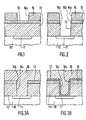
- the method according to the invention relates to the production of an interconnection configuration on a semiconductor device, a portion of which has been shown diagrammatically in FIG. 1.
- a silicon substrate 10 for example, the different active elements of an integrated circuit have been developed, the different stages of the method which will be described having the aim of making electrical contact with an active region 11 of the device which can for example be a source or drain region of a MOS type field effect transistor.
- an insulating layer 12 has been formed, most often made of silica glass optionally doped with phosphorus or boron.
- the insulating layer 12 has a relatively large thickness of 1 '' from 0.8 to 1 ⁇ m.
- the insulating layer 12 is covered with a so-called separation layer 13 of a nature such that it can be pickled selectively with respect to the insulating layer 12.
- the thickness of this layer can vary but nevertheless it is generally between 50 nm and 300 nm.
- the entire device was then covered with a mask 15 of photosensitive lacquer in which openings 16a were created at the locations where contacts must be created.
- an opening 16b has been successively etched in the separation layer 13 and an opening 16c in the insulating layer 12, the opening 16c having a depth such that the surface of the active region 11 is discovered.
- the diameter of the contact openings such as 16c is for example 0.8 ⁇ m, so that these openings have an aspect ratio equal to or slightly greater than 1.
- pickling by reactive ions is used.
- the separating layer 13 has a thickness such that the opening 16b which is formed therein has an aspect ratio much less than 1 and that consequently, the question of the angle of the walls of this opening 16b is not as important as for opening 16c in insulating layer 12.
- FIG. 3A corresponding to the stage of the method in which a layer of conductive material 18 has been deposited which is thick enough for the contact opening 16b, 16c to be completely filled with this conductive material.
- a known method is used to provide a good surface covering, including surfaces which are internal to the contact openings.
- these known methods is the so-called chemical vapor deposition method, at reduced pressure (LPCVD) or even at atmospheric pressure (CVD).
- LPCVD reduced pressure
- CVD atmospheric pressure
- the conductive material 18 tungsten can be chosen, an alloy of tungsten and titanium, an alloy of tungsten and silicon, or polycrystalline silicon highly doped to be sufficiently conductive.
- the pickling of the conductive material 18 is preferably carried out in a plasma, the nature of which depends on the nature of the conductive material used.
- a plasma the nature of which depends on the nature of the conductive material used.
- tungsten or of an alloy rich in tungsten use will be made, for example, of a sulfur hexafluoride plasma (SF6).
- SF6 sulfur hexafluoride plasma
- the level of the element 18a of conductive material may therefore be somewhat below the level of the separation layer 13 at the after the pickling operation.
- the stopping of the attack is defined either by a precise control of the etching time, or by any detection means in particular using the variation of intensity of a particular plasma emission line.
- the following operation consisting in eliminating the separation layer 13 is done selectively with respect to the insulating layer 12. Consequently, the surface of the insulating layer 12, thus freed, is free from any irregularity independently of the possible roughness of the surface of the separation layer 13.
- the material of the separation layer 13 will have been chosen so that it can be removed selectively with respect to the conductive material 18.
- the upper level 20 of the element 18a of conductive material can be made higher, if desired, compared to the level 21 of the surface of the insulating layer 12. Such an offset is provided by difference due to the thickness of the separating layer 13 which is eliminated.
- the separation layer 13 is made of silicon nitride (Si3N4).
- Si3N4 silicon nitride
- the separation layer 13 does not constitute a pickling barrier but on the contrary is attacked at a speed which is of the same order of magnitude as the attack speed of the material conductor 18 in the case where the latter is tungsten or an alloy rich in tungsten.
- the metal layer 22 is produced for example from aluminum or an aluminum-silicon alloy and / or aluminum-copper with a thickness close to 1 ⁇ m, a layer in which the interconnection configuration is carried out by the usual photomasking and etching methods. .
- the material used to form the separation layer 13 is of such a nature that the conductive material 18 can be pickled selectively with respect to this separation layer 13.
- the separation layer 13 preferably uses aluminum or an aluminum alloy or cobalt.
- the separation layer 13 then constitutes a stop layer at the end of this stripping.
- the attack on the conductive material 18 is prolonged, the separation layer 13 is not attacked, which is why it can be given a thickness slightly smaller than in the embodiment described above.
- a thickness chosen between 50 and 150 nm is entirely suitable.
- the separation layer 13 When the separation layer 13 is made of aluminum or aluminum alloy, it can be selectively eliminated with respect to the insulating layer 12 and with respect to the conductive filling material 18 by means of dry etching using a plasma rich in ions. chlorine. It can also be carried out wet, in a solution based on orthophosphoric acid commonly used by specialists in the field.
- the separation layer 13 is made of cobalt, to selectively remove this layer, a wet pickling is then used, for example by means of a mixture of three parts of 30% HCl and one part of H2O2, ambient temperature.
- the pickling selectivity of the separation layer 13 relative to the insulating layer 12 is taken advantage of during the etching of the contact openings 16C.
- the separation layer 13 is made of aluminum or cobalt and after having produced an opening 16b in this layer using an appropriate pickling in the presence of the photosensitive lacquer mask 15 (see FIG. 2), the openings 16c are etched. through the insulating layer 12. As indicated above, this etching is preferably carried out by pickling reactive ions rich in fluorine.
- the separation layer 13 with its opening 16b constitutes a mask more resistant to this etching than the photosensitive lacquer mask 15 itself.
- the latter can optionally be deleted before the etching of the contact openings, but it can also be kept.
- a separating layer 13 as an additional mask for the etching of the contact openings 16c in the insulating layer 12, the etching of narrow and deep contact openings is facilitated as well as obtaining walls of practically vertical openings.
- FIG. 3B illustrates an alternative embodiment of the method according to the invention.
- the filling of the contact openings 16b, 16c with a conductive material is carried out by first depositing a thin layer of titanium-tungsten alloy as an adhesion and covering layer for the entire surface including the interior surface. of the contact opening 16c, then by depositing a thick layer of tungsten 28 which provides the effective filling of the contact openings.
- the tungsten layer 28 is produced by chemical vapor deposition at reduced pressure (LPCVD) while the titanium-tungsten alloy layer 27 is deposited by sputtering with a thickness of the order of 100 nm.
- Other materials can also be used for this purpose, in particular a tungsten-silicon alloy, titanium, titanium nitride, or a refractory metal silicide.
- FIG. 4B corresponds to a later stage of the process, equivalent to that of FIG. 4A and in which the same reference numerals designate similar elements.
- FIG. 5B illustrates the later stage of the process which corresponds to that of FIG. 5A in which the separation layer 13 has been removed while a metallic interconnection layer 22 overcomes the structure and is in contact with the localized element of conductive materials 28a, 27a.
- the removal of the separation layer 13 makes it possible to raise the level 20 of the element 28a of the conductive filling material with respect to the level 21 of the insulating layer 12.
- the separation layer 13 can be formed from one of the materials already mentioned above, that is to say silicon nitride, aluminum, an aluminum alloy or cobalt.
- the method according to the invention is not limited to the manufacture of an interconnection structure on an integrated circuit with an MOS transistor, it is more generally aimed at making contacts on all kinds of semiconductor devices when it is desired to use zones contact and very small contact openings.
Landscapes
- Internal Circuitry In Semiconductor Integrated Circuit Devices (AREA)
Applications Claiming Priority (2)
| Application Number | Priority Date | Filing Date | Title |
|---|---|---|---|
| FR8805391A FR2630588A1 (fr) | 1988-04-22 | 1988-04-22 | Procede pour realiser une configuration d'interconnexion sur un dispositif semiconducteur notamment un circuit a densite d'integration elevee |
| FR8805391 | 1988-04-22 |
Publications (2)
| Publication Number | Publication Date |
|---|---|
| EP0343698A1 true EP0343698A1 (de) | 1989-11-29 |
| EP0343698B1 EP0343698B1 (de) | 1994-07-20 |
Family
ID=9365595
Family Applications (1)
| Application Number | Title | Priority Date | Filing Date |
|---|---|---|---|
| EP89200972A Expired - Lifetime EP0343698B1 (de) | 1988-04-22 | 1989-04-17 | Herstellungsverfahren für Verbindungsstrukturen auf einem Halbleiterbauelement, besonders auf einem hochintegrierten Schaltkreis |
Country Status (6)
| Country | Link |
|---|---|
| US (2) | US4936950A (de) |
| EP (1) | EP0343698B1 (de) |
| JP (1) | JP2604631B2 (de) |
| KR (1) | KR0138913B1 (de) |
| DE (1) | DE68916859T2 (de) |
| FR (1) | FR2630588A1 (de) |
Cited By (6)
| Publication number | Priority date | Publication date | Assignee | Title |
|---|---|---|---|---|
| EP0542263A1 (de) * | 1991-11-12 | 1993-05-19 | Nec Corporation | Halbleiterbauelement und niedrigen Widerstandswerken an Verbindungsstellen der leitenden Schichten |
| DE4301451A1 (de) * | 1992-01-24 | 1993-08-05 | Micron Technology Inc | |
| EP0571691A1 (de) * | 1992-05-27 | 1993-12-01 | STMicroelectronics S.r.l. | Verdrahtung auf Wolfram-Plomben |
| WO1994003926A1 (de) * | 1992-08-10 | 1994-02-17 | Robert Bosch Gmbh | Halbleiteranordnung |
| EP0660393A1 (de) * | 1993-12-23 | 1995-06-28 | STMicroelectronics, Inc. | Verfahren und Dielektricumstruktur zur Erleichterung des Metalüberätzung ohne Beschädigung des Zwischendielektricum |
| WO2008007256A3 (en) * | 2006-06-21 | 2008-05-29 | Nxp Bv | Semiconductor device for low-power applications and a method of manufacturing thereof |
Families Citing this family (43)
| Publication number | Priority date | Publication date | Assignee | Title |
|---|---|---|---|---|
| US5103557A (en) * | 1988-05-16 | 1992-04-14 | Leedy Glenn J | Making and testing an integrated circuit using high density probe points |
| US6288561B1 (en) * | 1988-05-16 | 2001-09-11 | Elm Technology Corporation | Method and apparatus for probing, testing, burn-in, repairing and programming of integrated circuits in a closed environment using a single apparatus |
| US5225771A (en) * | 1988-05-16 | 1993-07-06 | Dri Technology Corp. | Making and testing an integrated circuit using high density probe points |
| JPH0242728A (ja) * | 1988-08-02 | 1990-02-13 | Sony Corp | 半導体装置の製造方法 |
| US5167760A (en) * | 1989-11-14 | 1992-12-01 | Intel Corporation | Etchback process for tungsten contact/via filling |
| US5035768A (en) * | 1989-11-14 | 1991-07-30 | Intel Corporation | Novel etch back process for tungsten contact/via filling |
| GB9015820D0 (en) * | 1990-07-18 | 1990-09-05 | Raychem Ltd | Processing microchips |
| KR930005238B1 (ko) * | 1990-10-25 | 1993-06-16 | 현대전자산업 주식회사 | 금속박막의 평탄화 형성방법 |
| JPH04257227A (ja) * | 1991-02-08 | 1992-09-11 | Sony Corp | 配線形成方法 |
| JPH04298030A (ja) * | 1991-03-27 | 1992-10-21 | Sony Corp | メタルプラグの形成方法 |
| US5137597A (en) * | 1991-04-11 | 1992-08-11 | Microelectronics And Computer Technology Corporation | Fabrication of metal pillars in an electronic component using polishing |
| US5164330A (en) * | 1991-04-17 | 1992-11-17 | Intel Corporation | Etchback process for tungsten utilizing a NF3/AR chemistry |
| US5124780A (en) * | 1991-06-10 | 1992-06-23 | Micron Technology, Inc. | Conductive contact plug and a method of forming a conductive contact plug in an integrated circuit using laser planarization |
| US5252516A (en) * | 1992-02-20 | 1993-10-12 | International Business Machines Corporation | Method for producing interlevel stud vias |
| JP2934353B2 (ja) * | 1992-06-24 | 1999-08-16 | 三菱電機株式会社 | 半導体装置およびその製造方法 |
| US5387315A (en) * | 1992-10-27 | 1995-02-07 | Micron Technology, Inc. | Process for deposition and etching of copper in multi-layer structures |
| US5486234A (en) * | 1993-07-16 | 1996-01-23 | The United States Of America As Represented By The United States Department Of Energy | Removal of field and embedded metal by spin spray etching |
| FR2711275B1 (fr) * | 1993-10-15 | 1996-10-31 | Intel Corp | Procédé automatiquement aligné de contact en fabrication de semi-conducteurs et dispositifs produits. |
| US5405806A (en) * | 1994-03-29 | 1995-04-11 | Motorola Inc. | Method for forming a metal silicide interconnect in an integrated circuit |
| JP2797994B2 (ja) * | 1995-02-17 | 1998-09-17 | ヤマハ株式会社 | 半導体装置 |
| US5658829A (en) * | 1995-02-21 | 1997-08-19 | Micron Technology, Inc. | Semiconductor processing method of forming an electrically conductive contact plug |
| US5580821A (en) * | 1995-02-21 | 1996-12-03 | Micron Technology, Inc. | Semiconductor processing method of forming an electrically conductive contact plug |
| US5534462A (en) * | 1995-02-24 | 1996-07-09 | Motorola, Inc. | Method for forming a plug and semiconductor device having the same |
| US6406998B1 (en) * | 1996-02-05 | 2002-06-18 | Micron Technology, Inc. | Formation of silicided contact by ion implantation |
| JP2812288B2 (ja) * | 1996-02-28 | 1998-10-22 | 日本電気株式会社 | 半導体装置の製造方法 |
| US6090700A (en) | 1996-03-15 | 2000-07-18 | Vanguard International Semiconductor Corporation | Metallization method for forming interconnects in an integrated circuit |
| US5658830A (en) * | 1996-07-12 | 1997-08-19 | Vanguard International Semiconductor Corporation | Method for fabricating interconnecting lines and contacts using conformal deposition |
| JPH10125865A (ja) | 1996-10-15 | 1998-05-15 | Fujitsu Ltd | 半導体装置、半導体記憶装置、およびその製造方法 |
| US5795831A (en) * | 1996-10-16 | 1998-08-18 | Ulvac Technologies, Inc. | Cold processes for cleaning and stripping photoresist from surfaces of semiconductor wafers |
| US5962346A (en) * | 1997-12-29 | 1999-10-05 | Taiwan Semiconductor Manufacturing Company, Ltd. | Fluorine-doped silicate glass hard mask to improve metal line etching profile |
| US6221775B1 (en) | 1998-09-24 | 2001-04-24 | International Business Machines Corp. | Combined chemical mechanical polishing and reactive ion etching process |
| JP4095731B2 (ja) | 1998-11-09 | 2008-06-04 | 株式会社ルネサステクノロジ | 半導体装置の製造方法及び半導体装置 |
| FR2795236B1 (fr) * | 1999-06-15 | 2002-06-28 | Commissariat Energie Atomique | Procede de realisation d'interconnexions notamment en cuivre pour dispositifs micro-electroniques |
| US6503827B1 (en) * | 2000-06-28 | 2003-01-07 | International Business Machines Corporation | Method of reducing planarization defects |
| JP2002093811A (ja) * | 2000-09-11 | 2002-03-29 | Sony Corp | 電極および半導体装置の製造方法 |
| KR100386083B1 (ko) * | 2000-09-22 | 2003-06-02 | 주식회사 하이닉스반도체 | 반도체 기판의 표면결함을 줄이는 방법 |
| DE10057463A1 (de) * | 2000-11-20 | 2002-05-29 | Promos Technologies Inc | Herstellungsverfahren für eine Metallleitung |
| JP4076131B2 (ja) * | 2002-06-07 | 2008-04-16 | 富士通株式会社 | 半導体装置の製造方法 |
| JP2005203476A (ja) * | 2004-01-14 | 2005-07-28 | Oki Electric Ind Co Ltd | 半導体装置の配線構造及びその製造方法 |
| KR100650811B1 (ko) * | 2005-05-30 | 2006-11-27 | 주식회사 하이닉스반도체 | 반도체 소자의 콘택 플러그 형성 방법 |
| KR100815186B1 (ko) | 2006-09-11 | 2008-03-19 | 주식회사 하이닉스반도체 | 돌출형상의 텅스텐플러그를 구비한 반도체소자의 제조 방법 |
| TWI340002B (en) * | 2008-04-07 | 2011-04-01 | Unimicron Technology Corp | Circuit board and manufacturing method thereof |
| CN102194993B (zh) * | 2010-03-11 | 2013-06-19 | 中芯国际集成电路制造(上海)有限公司 | 相变存储器存储单元的制作方法 |
Citations (1)
| Publication number | Priority date | Publication date | Assignee | Title |
|---|---|---|---|---|
| WO1987004858A1 (en) * | 1986-01-30 | 1987-08-13 | Plessey Overseas Limited | Method for producing integrated circuit interconnects |
Family Cites Families (14)
| Publication number | Priority date | Publication date | Assignee | Title |
|---|---|---|---|---|
| US4184909A (en) * | 1978-08-21 | 1980-01-22 | International Business Machines Corporation | Method of forming thin film interconnection systems |
| JPS55102235A (en) * | 1979-01-29 | 1980-08-05 | Nippon Telegr & Teleph Corp <Ntt> | Formation of interlayer conductive layer |
| US4361599A (en) * | 1981-03-23 | 1982-11-30 | National Semiconductor Corporation | Method of forming plasma etched semiconductor contacts |
| GB2137808A (en) * | 1983-04-06 | 1984-10-10 | Plessey Co Plc | Integrated circuit processing method |
| JPS6017933A (ja) * | 1983-07-11 | 1985-01-29 | Toshiba Corp | 半導体装置の製造方法 |
| US4484978A (en) * | 1983-09-23 | 1984-11-27 | Fairchild Camera & Instrument Corp. | Etching method |
| FR2563048B1 (fr) * | 1984-04-13 | 1986-05-30 | Efcis | Procede de realisation de contacts d'aluminium a travers une couche isolante epaisse dans un circuit integre |
| FR2566181B1 (fr) * | 1984-06-14 | 1986-08-22 | Commissariat Energie Atomique | Procede d'autopositionnement d'une ligne d'interconnexion sur un trou de contact electrique d'un circuit integre |
| US4640738A (en) * | 1984-06-22 | 1987-02-03 | International Business Machines Corporation | Semiconductor contact protection |
| JP2519217B2 (ja) * | 1985-09-11 | 1996-07-31 | テキサス インスツルメンツ インコ−ポレイテツド | 相互接続導体を形成する方法 |
| JPS6334954A (ja) * | 1986-07-29 | 1988-02-15 | Nec Corp | 半導体装置およびその製造方法 |
| JPS6376457A (ja) * | 1986-09-19 | 1988-04-06 | Fujitsu Ltd | 半導体装置の製造方法 |
| JPS63283161A (ja) * | 1987-05-15 | 1988-11-21 | Toshiba Corp | 半導体装置とその製造方法 |
| US4981550A (en) * | 1987-09-25 | 1991-01-01 | At&T Bell Laboratories | Semiconductor device having tungsten plugs |
-
1988
- 1988-04-22 FR FR8805391A patent/FR2630588A1/fr active Pending
-
1989
- 1989-04-14 US US07/339,029 patent/US4936950A/en not_active Ceased
- 1989-04-17 DE DE68916859T patent/DE68916859T2/de not_active Expired - Fee Related
- 1989-04-17 EP EP89200972A patent/EP0343698B1/de not_active Expired - Lifetime
- 1989-04-18 JP JP1098664A patent/JP2604631B2/ja not_active Expired - Fee Related
- 1989-04-19 KR KR1019890005132A patent/KR0138913B1/ko not_active Expired - Fee Related
-
1992
- 1992-05-11 US US07/880,860 patent/USRE34583E/en not_active Expired - Lifetime
Patent Citations (1)
| Publication number | Priority date | Publication date | Assignee | Title |
|---|---|---|---|---|
| WO1987004858A1 (en) * | 1986-01-30 | 1987-08-13 | Plessey Overseas Limited | Method for producing integrated circuit interconnects |
Non-Patent Citations (5)
| Title |
|---|
| 1986 PROCEEDINGS THIRD INTERNATIONAL IEEE VLSI MULTILEVEL INTERCONNECTION CONFERENCE, Santa Clara, CA, 9-10 juin 1986, pages 403-410, IEEE; G.C. SMITH et al: "Comparison of two contact plug techniques for use with planarized oxide" * |
| 1987 PROCEEDINGS FOURTH INTERNATIONAL IEEE VLSI MULTILEVEL INTERCONNECTION CONFERENCE, 15-16 juin 1987, Santa Clara, CA, pages 292-297, IEEE; R.W. WU et al.: "A reliable LPCVD tungsten interconnection process utilizing polyimide/plasma nitride as an interlayer dielectric" * |
| 1987 PROCEEDINGS FOURTH INTERNATIONAL IEEE VLSI MULTILEVEL INTERCONNECTION CONFERENCE, Santa Clara, CA, 15-16 juin 1987, pages 193-199, IEEE; J.-J. LEE et al.: "A study of tungsten etchback for contact and via fill applications" * |
| IBM TECHNICAL DISCLOSURE BULLETIN, vol. 24, no. 10, mars 1982, pages 5133-5134, New York, US; S. BOYAR et al.: "Quartz trench rie etch stop" * |
| IBM TECHNICAL DISCLOSURE BULLETIN, vol. 29, no. 9, février 1987, pages 3925-3927, New York, US; "Contact via definition where quartz insulation of metal lines is required" * |
Cited By (12)
| Publication number | Priority date | Publication date | Assignee | Title |
|---|---|---|---|---|
| EP0542263A1 (de) * | 1991-11-12 | 1993-05-19 | Nec Corporation | Halbleiterbauelement und niedrigen Widerstandswerken an Verbindungsstellen der leitenden Schichten |
| DE4301451A1 (de) * | 1992-01-24 | 1993-08-05 | Micron Technology Inc | |
| DE4301451C2 (de) * | 1992-01-24 | 1999-12-02 | Micron Technology Inc | Verfahren zur Bildung eines leitfähigen Stopfens in einer Isolierschicht |
| USRE39126E1 (en) | 1992-01-24 | 2006-06-13 | Micron Technology, Inc. | Two-step chemical mechanical polishing process for producing flush and protruding tungsten plugs |
| EP0571691A1 (de) * | 1992-05-27 | 1993-12-01 | STMicroelectronics S.r.l. | Verdrahtung auf Wolfram-Plomben |
| US5407861A (en) * | 1992-05-27 | 1995-04-18 | Sgs-Thomson Microelectronics, S.R.L. | Metallization over tungsten plugs |
| US5786272A (en) * | 1992-05-27 | 1998-07-28 | Sgs-Thomson Microelectronics S.R.L. | Metallization over tungsten plugs |
| WO1994003926A1 (de) * | 1992-08-10 | 1994-02-17 | Robert Bosch Gmbh | Halbleiteranordnung |
| EP0660393A1 (de) * | 1993-12-23 | 1995-06-28 | STMicroelectronics, Inc. | Verfahren und Dielektricumstruktur zur Erleichterung des Metalüberätzung ohne Beschädigung des Zwischendielektricum |
| US5766974A (en) * | 1993-12-23 | 1998-06-16 | Sgs-Thomson Microelectronics, Inc. | Method of making a dielectric structure for facilitating overetching of metal without damage to inter-level dielectric |
| WO2008007256A3 (en) * | 2006-06-21 | 2008-05-29 | Nxp Bv | Semiconductor device for low-power applications and a method of manufacturing thereof |
| US7985673B2 (en) | 2006-06-21 | 2011-07-26 | Nxp B.V. | Semiconductor device for low-power applications and a method of manufacturing thereof |
Also Published As
| Publication number | Publication date |
|---|---|
| FR2630588A1 (fr) | 1989-10-27 |
| JP2604631B2 (ja) | 1997-04-30 |
| JPH0212917A (ja) | 1990-01-17 |
| DE68916859D1 (de) | 1994-08-25 |
| DE68916859T2 (de) | 1995-02-16 |
| EP0343698B1 (de) | 1994-07-20 |
| USRE34583E (en) | 1994-04-12 |
| KR0138913B1 (ko) | 1998-06-01 |
| KR900017172A (ko) | 1990-11-15 |
| US4936950A (en) | 1990-06-26 |
Similar Documents
| Publication | Publication Date | Title |
|---|---|---|
| EP0343698B1 (de) | Herstellungsverfahren für Verbindungsstrukturen auf einem Halbleiterbauelement, besonders auf einem hochintegrierten Schaltkreis | |
| EP0351001B1 (de) | Verfahren zur Herstellung einer Halbleitervorrichtung mit mindestens einer kleine Kontaktlöcher enthaltenden Leiterbahn | |
| EP0325808B1 (de) | Verfahren, um eine elektrische Verbindung auf einer Silizium-Halbleitervorrichtung herzustellen | |
| EP0498717A1 (de) | Verfahren zur vergrabenen lokalisierten Oxidation eines Siliziumsubstrates und deren entsprechende integrierte Schaltung | |
| EP0528713A1 (de) | Verfahren zur Kontrolle der Ätzkontur einer Schicht einer integrierten Schaltung | |
| EP1030353A1 (de) | Anisotropes Plasmaätzen von dielektrischen, organisch- polymeren Materialien | |
| EP0372644B1 (de) | Verfahren zum Herstellen einer integrierten Schaltung einschliesslich Schritte zum Herstellen einer Verbindung zwischen zwei Schichten | |
| EP0216425B1 (de) | Verfahren zum Einebnen der Oberfläche einer Halbleitervorrichtung, die Siliziumnitrid als isolierendes Material verwendet | |
| FR2785721A1 (fr) | Procede de fabrication d'une structure semi-conductrice | |
| FR2763424A1 (fr) | Processus de damasquinage double | |
| EP2690655B1 (de) | Verfahren zur Herstellung von Durchkontaktierungen | |
| EP0275595B1 (de) | Verfahren zur Herstellung von Verbindungslinien und von Kreuzungspunkten verschiedener Metallisierungsebenen auf einer integrierten Schaltung | |
| EP0951067B1 (de) | Integrierte Schaltung mit einer Ätz-Stoppschicht und Herstellungsverfahren | |
| FR2855324A1 (fr) | Procede de fabrication d'une interconnexion pour un dispositif a semiconducteur | |
| EP0904599B1 (de) | VERFAHREN ZUM ÄTZEN DES GATES IN MOS TECHNOLOGIE UNTER VERWENDUNG EINER HARTEN MASKE AUF DER BASIS VON SiON | |
| EP0975018A1 (de) | Methode zur Herstellung eines Kondensators in einer integrierten Schaltung | |
| FR2776126A1 (fr) | Procede de formation d'une isolation par tranchee depourvue de partie vide | |
| EP0338636A1 (de) | Verfahren zum Herstellen von elektrischen Kontakten von kleiner Dimension auf einer Halbleiterschaltung | |
| EP0336461B1 (de) | Planarisierungsverfahren der Oberflächen von Halbleiterbauelementen | |
| EP1146550A2 (de) | Verfahren zur Herstellung von Verbindungsleitungen in einem integrierten Schaltkreis | |
| FR2844396A1 (fr) | Procede de realisation d'un composant electronique integre et dispositif electrique incorporant un composant integre ainsi obtenu | |
| EP4006997B1 (de) | Verfahren zur herstellung einer quantenvorrichtung | |
| EP0443967B1 (de) | Verfahren zur mechanischen Abhebung einer Metallschicht auf einem Polymer | |
| EP0548351B1 (de) | Verfahren zur herstellung integrierter schaltungen mit nebeneinander geformten elektroden | |
| KR100646964B1 (ko) | 반도체 소자의 금속배선 형성방법 |
Legal Events
| Date | Code | Title | Description |
|---|---|---|---|
| PUAI | Public reference made under article 153(3) epc to a published international application that has entered the european phase |
Free format text: ORIGINAL CODE: 0009012 |
|
| AK | Designated contracting states |
Kind code of ref document: A1 Designated state(s): DE FR GB IT NL |
|
| 17P | Request for examination filed |
Effective date: 19900523 |
|
| 17Q | First examination report despatched |
Effective date: 19920709 |
|
| GRAA | (expected) grant |
Free format text: ORIGINAL CODE: 0009210 |
|
| AK | Designated contracting states |
Kind code of ref document: B1 Designated state(s): DE FR GB IT NL |
|
| PG25 | Lapsed in a contracting state [announced via postgrant information from national office to epo] |
Ref country code: NL Effective date: 19940720 |
|
| REF | Corresponds to: |
Ref document number: 68916859 Country of ref document: DE Date of ref document: 19940825 |
|
| ITF | It: translation for a ep patent filed | ||
| GBT | Gb: translation of ep patent filed (gb section 77(6)(a)/1977) |
Effective date: 19940908 |
|
| NLV1 | Nl: lapsed or annulled due to failure to fulfill the requirements of art. 29p and 29m of the patents act | ||
| ITPR | It: changes in ownership of a european patent |
Owner name: CAMBIO RAGIONE SOCIALE;PHILIPS ELECTRONICS N.V. |
|
| PLBE | No opposition filed within time limit |
Free format text: ORIGINAL CODE: 0009261 |
|
| STAA | Information on the status of an ep patent application or granted ep patent |
Free format text: STATUS: NO OPPOSITION FILED WITHIN TIME LIMIT |
|
| REG | Reference to a national code |
Ref country code: FR Ref legal event code: CD |
|
| 26N | No opposition filed | ||
| REG | Reference to a national code |
Ref country code: FR Ref legal event code: CD |
|
| REG | Reference to a national code |
Ref country code: GB Ref legal event code: IF02 |
|
| REG | Reference to a national code |
Ref country code: GB Ref legal event code: 746 Effective date: 20021025 |
|
| REG | Reference to a national code |
Ref country code: FR Ref legal event code: D6 |
|
| PGFP | Annual fee paid to national office [announced via postgrant information from national office to epo] |
Ref country code: FR Payment date: 20030424 Year of fee payment: 15 |
|
| PGFP | Annual fee paid to national office [announced via postgrant information from national office to epo] |
Ref country code: GB Payment date: 20030430 Year of fee payment: 15 |
|
| PGFP | Annual fee paid to national office [announced via postgrant information from national office to epo] |
Ref country code: DE Payment date: 20030616 Year of fee payment: 15 |
|
| PG25 | Lapsed in a contracting state [announced via postgrant information from national office to epo] |
Ref country code: GB Free format text: LAPSE BECAUSE OF NON-PAYMENT OF DUE FEES Effective date: 20040417 |
|
| PG25 | Lapsed in a contracting state [announced via postgrant information from national office to epo] |
Ref country code: DE Free format text: LAPSE BECAUSE OF NON-PAYMENT OF DUE FEES Effective date: 20041103 |
|
| GBPC | Gb: european patent ceased through non-payment of renewal fee |
Effective date: 20040417 |
|
| PG25 | Lapsed in a contracting state [announced via postgrant information from national office to epo] |
Ref country code: FR Free format text: LAPSE BECAUSE OF NON-PAYMENT OF DUE FEES Effective date: 20041231 |
|
| REG | Reference to a national code |
Ref country code: FR Ref legal event code: ST |
|
| PG25 | Lapsed in a contracting state [announced via postgrant information from national office to epo] |
Ref country code: IT Free format text: LAPSE BECAUSE OF NON-PAYMENT OF DUE FEES;WARNING: LAPSES OF ITALIAN PATENTS WITH EFFECTIVE DATE BEFORE 2007 MAY HAVE OCCURRED AT ANY TIME BEFORE 2007. THE CORRECT EFFECTIVE DATE MAY BE DIFFERENT FROM THE ONE RECORDED. Effective date: 20050417 |