EP0341472A2 - Ultramicro-électrode et procédé pour sa fabrication - Google Patents
Ultramicro-électrode et procédé pour sa fabrication Download PDFInfo
- Publication number
- EP0341472A2 EP0341472A2 EP89107309A EP89107309A EP0341472A2 EP 0341472 A2 EP0341472 A2 EP 0341472A2 EP 89107309 A EP89107309 A EP 89107309A EP 89107309 A EP89107309 A EP 89107309A EP 0341472 A2 EP0341472 A2 EP 0341472A2
- Authority
- EP
- European Patent Office
- Prior art keywords
- layer
- ultramicroelectrode
- insulating layer
- ion
- fiber
- Prior art date
- Legal status (The legal status is an assumption and is not a legal conclusion. Google has not performed a legal analysis and makes no representation as to the accuracy of the status listed.)
- Ceased
Links
Images

Classifications
-
- G—PHYSICS
- G01—MEASURING; TESTING
- G01N—INVESTIGATING OR ANALYSING MATERIALS BY DETERMINING THEIR CHEMICAL OR PHYSICAL PROPERTIES
- G01N27/00—Investigating or analysing materials by the use of electric, electrochemical, or magnetic means
- G01N27/26—Investigating or analysing materials by the use of electric, electrochemical, or magnetic means by investigating electrochemical variables; by using electrolysis or electrophoresis
- G01N27/28—Electrolytic cell components
- G01N27/30—Electrodes, e.g. test electrodes; Half-cells
- G01N27/308—Electrodes, e.g. test electrodes; Half-cells at least partially made of carbon
-
- Y—GENERAL TAGGING OF NEW TECHNOLOGICAL DEVELOPMENTS; GENERAL TAGGING OF CROSS-SECTIONAL TECHNOLOGIES SPANNING OVER SEVERAL SECTIONS OF THE IPC; TECHNICAL SUBJECTS COVERED BY FORMER USPC CROSS-REFERENCE ART COLLECTIONS [XRACs] AND DIGESTS
- Y10—TECHNICAL SUBJECTS COVERED BY FORMER USPC
- Y10T—TECHNICAL SUBJECTS COVERED BY FORMER US CLASSIFICATION
- Y10T428/00—Stock material or miscellaneous articles
- Y10T428/12—All metal or with adjacent metals
- Y10T428/12493—Composite; i.e., plural, adjacent, spatially distinct metal components [e.g., layers, joint, etc.]
- Y10T428/12535—Composite; i.e., plural, adjacent, spatially distinct metal components [e.g., layers, joint, etc.] with additional, spatially distinct nonmetal component
- Y10T428/12556—Organic component
- Y10T428/12569—Synthetic resin
-
- Y—GENERAL TAGGING OF NEW TECHNOLOGICAL DEVELOPMENTS; GENERAL TAGGING OF CROSS-SECTIONAL TECHNOLOGIES SPANNING OVER SEVERAL SECTIONS OF THE IPC; TECHNICAL SUBJECTS COVERED BY FORMER USPC CROSS-REFERENCE ART COLLECTIONS [XRACs] AND DIGESTS
- Y10—TECHNICAL SUBJECTS COVERED BY FORMER USPC
- Y10T—TECHNICAL SUBJECTS COVERED BY FORMER US CLASSIFICATION
- Y10T428/00—Stock material or miscellaneous articles
- Y10T428/31504—Composite [nonstructural laminate]
- Y10T428/31678—Of metal
- Y10T428/31692—Next to addition polymer from unsaturated monomers
Definitions
- the invention relates to an ultramicroelectrode with a conductor made of precious metal wire or carbon fiber and an insulating layer arranged thereon, a method for its production and its use.
- Ultramicroelectrodes consist of very thin electrical conductors in the form of fibers or wires with a diameter of a few ⁇ m and an insulating layer arranged on them. Such microelectrodes are required to be able to be used in a wide range of solvents, to be simple to build, to have accurate dimensional dimensions and to be used repeatedly.
- the insulating layer of conventional ultra-microelectrodes is made of glass or an epoxy resin. Such ultramicroelectrodes are described in the following references:
- Such ultramicroelectrodes are usually produced by pulling a glass tube to a capillary and inserting a wire or a fiber made of noble metal or carbon into the capillary thus drawn and welding it therein.
- the thickness of the insulating layer made of glass or epoxy resin is approximately 1 to 2 mm, and it is difficult to form a uniform layer thickness over the entire length of the electrode.
- Ultramicroelectrodes with glass insulation are also very fragile, because the different thermal expansion coefficients of glass and fiber material lead to the formation of hairline cracks in the glass when subjected to thermal stress. These hairline cracks are the reason for a relatively large enlargement of the electrode surface as well as for non-linear diffusion and for edge effects. Furthermore, the poor adhesion of the encapsulation material for both glass and epoxy resins on the wire or fiber leads to the penetration of the liquid under the insulation layer. Furthermore, epoxy resins have poor stability to organic solvents, since components of the resin are dissolved out. This leads to degradation or aging of the epoxy resin. All these Effects lead to an increase in the residual current component and thus to an increase in the double-layer capacity of the insulator material.
- an object of the present invention to provide an ultramicroelectrode which is stable in use and has an insulating layer which is resistant to chemical and mechanical influences and has a low double-layer capacity, which allows a fault-free evaluation of the measurement signal even with a very fast measurement signal recording.
- This ultramicroelectrode can be manufactured with high productivity, reproducibility and improved uniformity of the layer formation.
- the insulator layer can be deposited uniformly regardless of the dimension of the electron conductor, has no cracks and has excellent adhesion properties.
- the insulating layer consists of a cross-linked poly-4-oxyphenylene, poly-4-thiophenylene or poly-4-aniline, a high breakdown voltage is achieved, with capacitive couplings of the insulating wall being kept small. As a result, the signal noise or leakage currents are largely suppressed when a measurement signal is recorded rapidly.
- a very thin and uniform layer thickness is achieved on the fiber or the wire, whereby an automatic production with high productivity and good reproducibility.
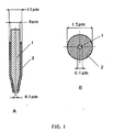
- FIG. 1A shows a longitudinal sectional view of a conically tapered ultramicroelectrode
- FIG. 1B explains a cross section of the microelectrode.
- the reference number 1 denotes a noble metal wire or a carbon fiber and the reference number 2 represents the insulating layer.
- the ultramicroelectrode is referred to as a disk ultramicroelectrode.
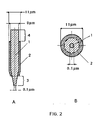
- FIGS. 2A and B A further embodiment of the ultramicroelectrode is shown in FIGS. 2A and B in the longitudinal or transverse layer.
- the ultramicroelectrode is referred to as a cylindrical ultramicroelectrode.
- the tip and the upper end region of the electrode (3) and (4) are free of insulating material.
- the ultramicroelectrode is called a bipolar ultramicroelectrode.
- the reference number (1) means a precious metal wire or a lenstoff fiber to which the insulating layer is applied (3).
- Reference number (2) denotes a metallic layer which is insulated from the conductive layer (6) required for further measurement signal derivation by epoxy (5).
- Reference number (4) means a glass capillary which is used as a holder. The lower area of the electrode (7) is free of metal.
- FIG. 3B Another embodiment of the ultramicroelectrode is also shown in longitudinal cross section in FIG. 3B.
- the ultramicroelectrode is called a shielded ultramicroelectrode.
- Reference numerals (1) to (6) have the same meanings as in Fig. 3A.
- the phenylene radicals are crosslinked in the ortho or meta position via alkylene groups having 2 to 10 carbon atoms.
- the alkylene groups are preferably 2 to 5 carbon atoms in length.
- the insulating layers are produced on the wire or the fiber by electrochemical polymerization of monomers containing phenol, thiophenol and / or aniline in an electrolyte bath, a polymer layer having a linear structure being initially formed.
- the monomers used must be blocked in the ortho position so that a linear polymer structure is formed.
- the phenyl radical of the monomer in the ortho position expediently has an aliphatic radical of up to 10 carbon atoms, preferably up to 5 carbon atoms, this aliphatic radical advantageously being unsaturated.
- a suitable unsaturated aliphatic radical has 2 to 10, preferably 2 to 5 carbon atoms and is preferably a vinyl or allyl group.
- Preferred monomers are 2-allylphenol, 2-allylthiophenol and 2-allylaniline or corresponding vinyl compounds.
- the electrochemical deposition is preferably carried out in an aqueous, alkaline environment at the anode.
- a water-alcohol mixture is preferably used, the mixing ratio (volume) being 1:10 to 10: 1, preferably 1: 5 to 5: 1.
- a lower aliphatic alcohol is preferred.
- the electrolyte solution contains an amine or an aqueous ammonia solution or a mixture of both in order to suppress the passivation of the electrode surface.
- the amine is a primary amine with an aliphatic group.
- the aliphatic group is expediently an alkyl group with 1 to 10 carbon atoms, which can also be unsaturated.
- Exemplary amines are allylamine and propylamine.
- the electrolyte solution preferably contains an adhesion improver in order to promote adhesion to the electrode surface.
- Suitable adhesion improvers are ethylene glycol monobutyl ether or butoxymethanol.
- the adhesion improver is used in a proportion of 1 to 10% by volume, based on the electrolyte solution.
- the electrochemical deposition takes place at 20 to 50 ° C., preferably at room temperature and at a constant potential of preferably 2 to 8 Volts, especially 4 to 6 volts.
- the unsaturated groups present are crosslinked by heating or radiation.
- a temperature treatment is expediently carried out, preferably at 120 to 200 ° C., in particular at 150 ° C.
- a suitable temperature can easily be determined using simple tests for a given polymer layer. Irradiation with UV rays is also possible.
- a suitable method consists in an electrochemical etching with a solution of ethylenediaminetetraacetate, NH4OH and H2O2 at a pulsating voltage of 0 to +2 V for about 5 to 10 min. Then a voltage of + 0.4 to - 0.4 V 10 min to the electrode in a 1 M KNO3 solution. long created.
- the thickness of the fiber or of the wire is expediently in the range from 0.1 to 15 ⁇ m, preferably 5 to 15 ⁇ m, in particular in the range from 8 to 10 ⁇ m. Since the ultramicroelectrode is expediently tapered at one end, the diameter of the electrode fiber at the tip can be up to 0.1 ⁇ m.
- the thickness of the insulating layer is expediently in the range from 1.0 to 3.0 ⁇ m, preferably in the range from 1.5 to 2.0 ⁇ m. It was found that the networked insulation layer with such a layer thickness gives the desired insulation effect.
- the end of the microelectrode is expediently designed as a disk, as shown in FIG. 1.
- the thickness of the insulating layer at the tip of the microelectrode can be equal to or less than the diameter of the fiber.
- the end regions are free of an insulating layer.
- Such an end region of the ultramicroelectrode free of the insulating layer can be achieved by chemically detaching the end of the polymer layer after the electrochemical deposition. This takes advantage of the fact that the uncrosslinked linear polymer is insoluble in the aqueous system, but is soluble in various organic solvents such as acetone.
- the microelectrode shown in FIG. 2 can also be produced by covering the tip of the electrode (3) with a galvanoresist or a metal before applying the insulating layer.
- the galvanoresist protects the area (3) during the electrochemical polymerization against deposition of the polymer layer. After the insulating layer (2) has been applied, the galvanoresist is chemically etched off again from the region (3). Commonly available products can be used as galvanoresist and etchant.
- the area (3) and (4) can be special which are covered precisely by chemical or electrochemical deposition of, for example, copper or nickel. These metals can also be chemically etched back after they have fulfilled their protective function.
- the end region (4) in Fig. 2A is coated with metal.
- Gold or silver filled conductive adhesives can also be used for metallization.
- the tip of the ultramicroelectrode free of insulating material which can be designed as a disk (see FIG. 1A) or as a cylinder (see FIG. 2A), is used for the use of the electrode in analytical measurement technology e.g. electrochemically metallized for inverse voltammetry, e.g. with mercury.
- the bipolar ultramicroelectrode shown in Fig. 3A is produced by either chemically and subsequently electrochemically or using a physical method, e.g. a metal layer (2) is applied by vapor deposition, preference being given to noble metals such as platinum, palladium or gold.
- the layer thickness of the metal layer is 0.2 to 5 ⁇ m, preferably 0.5 to 1 ⁇ m.
- Chemical metallization can be done using a process for electroless copper plating of non-conductive materials that is commercially available. Because the outer metal layer (2) as a counter electrode to the inner disk or cylindrical ultramicroelectrode (1), a sufficiently large area (7) must be kept free of metal between the working electrode (inner conductor, for example carbon fiber) and counter electrode (outer conductor - metal) Avoid short circuits. The distance between the working and counter electrodes depends on the conductivity of the electrolyte; a distance of less than 2 mm is expediently chosen.
- the metal-free insulated area is either masked before the chemical copper plating or the copper which has already been deposited is chemically or electrochemically etched away.
- a suitable commercially available galvanoresist or etching resist can be used for masking.
- the remaining copper layer is then electrochemically reinforced with precious metals such as gold, platinum or palladium.
- the above-mentioned area between the working electrode and counterelectrode which is to be kept free of metal can either be covered mechanically beforehand with a mask or coated with a layer (etching resist or galvanoresist) which is subsequently coated is chemically detached. Chemical or electrochemical detachment of the applied precious metal layer is also possible.
- a metallic intermediate layer such as e.g. a Ti / W alloy, chromium or vanadium is used.
- the choice of the intermediate layer depends on the precious metal used.
- the shielded ultramicroelectrode shown in Fig. 3B is produced like the ultramicroelectrode shown schematically in FIG. 3A without the lower end region being free of metal.
- a polymer layer is deposited on the metal layer (2) and then crosslinked to form an insulator.
- the metal layer (2) is grounded and serves as a shield.
- the shielding is preferred for ultramicroelectrodes with a very small electroactive area, in which currents flow in the picoampere range and for measurements in the MHz range.
- the ultramicroelectrodes explained above can be used in particular in the biochemical and medical fields, for example as amperometric or potentiometric sensors or as stimulation electrodes or as electrodes in analytical measurement technology, e.g. for the inverse voltammetry.
- the ultramicroelectrodes can be used as potentiometric microsensors.
- one of the areas of the ultramicroelectrode free of the insulating layer is provided with an ion-selective layer which contains an ion-selective material.
- Suitable ion-selective materials are, for example, salts, poorly soluble metals or exchange resins, crown ethers, complexing agents, etc., which are embedded in the matrix of a polymer (e.g. PVC, silicone rubber, etc.).
- Ion-selective layers have a membrane function and only let the substance to be determined that is to be detected potentiometrically via the conductor. The ion-selective layer must therefore not be completely insulating.
- the ion-selective layer contains as matrix a copolymer of monomers containing phenol, thiophenol and / or aniline with an unsaturated aliphatic group in the ortho position with at least a non-crosslinkable OH-, NH2- or SH-containing aromatic comonomer, the copolymer being formed by electrochemical deposition and subsequent crosslinking, as explained above for the insulating layer.
- the ion-selective material can be incorporated into the copolymer layer as part of the electrolyte solution during electrochemical deposition or after crosslinking by soaking.
- the electrochemical deposition is formed in the presence of a non-crosslinkable OH, NH or SH-containing aromatic comonomer.
- a suitable comonomer is a phenol, thiophenol or aniline with a saturated alkyl group with 1 to 10 carbon atoms in the ortho position. The alkyl group advantageously has 1 to 5 carbon atoms.
- a suitable comonomer is o-cresol or ethylphenol.
- the non-crosslinkable comonomer is used in a proportion of preferably at least 40 mol% of the total monomers, in particular in a proportion of 50 to 80 mol%.
- the proportion of the monomer having an unsaturated aliphatic group is correspondingly 60 mol% or less, in particular 20 to 50 mol%.
- the proportion of the ion-selective material in the layer is advantageously 0.5 to 5% by weight, based on the matrix material.
- the thickness of the ion-selective layer is 1 to 3 ⁇ m, preferably 1.5 to 2 ⁇ m.
- a carbon fiber with a diameter of 8 ⁇ m, with one end tapered was anodically coated in the following electrolytic solution. 0.23 mol / l 2-allylphenol 0.40 mol / l Allylamine or ammonia 0.20 mol / l Cellosolve (ethylene glycol monobutyl ether) dissolved in methanol and water 1: 1 (parts by volume)
- the electrochemical polymerization was carried out at a constant potential of 4 V at room temperature for 30 minutes.
- the polymer layer is then heated in an oven at 150 ° C., as a result of which the deposited polymer layer is crosslinked.
- the insulating layer formed had a layer thickness of 1.5 ⁇ m, which is sufficient for the insulation.
- the measured DC resistance was 2 M ⁇ .
- the breakdown voltage in a 1 M KCl solution is greater than 106 V / cm.
- the capacitance of the insulating layer was approximately 1 pF. Due to the low double-layer capacitance, the signal-to-noise ratio is very low during the recording of the measured values, which enables rapid signal recording.
Landscapes
- Chemical & Material Sciences (AREA)
- Life Sciences & Earth Sciences (AREA)
- Health & Medical Sciences (AREA)
- Biochemistry (AREA)
- General Physics & Mathematics (AREA)
- Electrochemistry (AREA)
- Physics & Mathematics (AREA)
- Analytical Chemistry (AREA)
- Molecular Biology (AREA)
- General Health & Medical Sciences (AREA)
- Chemical Kinetics & Catalysis (AREA)
- Immunology (AREA)
- Pathology (AREA)
- Electrolytic Production Of Non-Metals, Compounds, Apparatuses Therefor (AREA)
- Inert Electrodes (AREA)
- Laminated Bodies (AREA)
- Investigating Or Analyzing Materials By The Use Of Electric Means (AREA)
- Macromolecular Compounds Obtained By Forming Nitrogen-Containing Linkages In General (AREA)
Applications Claiming Priority (2)
| Application Number | Priority Date | Filing Date | Title |
|---|---|---|---|
| DE3816458A DE3816458A1 (de) | 1988-05-13 | 1988-05-13 | Ultramikroelektrode, verfahren zu deren herstellung und ihre verwendung |
| DE3816458 | 1988-05-13 |
Publications (2)
| Publication Number | Publication Date |
|---|---|
| EP0341472A2 true EP0341472A2 (fr) | 1989-11-15 |
| EP0341472A3 EP0341472A3 (fr) | 1991-10-23 |
Family
ID=6354364
Family Applications (1)
| Application Number | Title | Priority Date | Filing Date |
|---|---|---|---|
| EP19890107309 Ceased EP0341472A3 (fr) | 1988-05-13 | 1989-04-25 | Ultramicro-électrode et procédé pour sa fabrication |
Country Status (4)
| Country | Link |
|---|---|
| US (1) | US4959130A (fr) |
| EP (1) | EP0341472A3 (fr) |
| JP (1) | JPH0273146A (fr) |
| DE (1) | DE3816458A1 (fr) |
Cited By (4)
| Publication number | Priority date | Publication date | Assignee | Title |
|---|---|---|---|---|
| DE4314007A1 (de) * | 1993-04-26 | 1994-10-27 | Elbau Elektronik Bauelemente G | Meßelektrodenanordnung |
| EP0668501A1 (fr) * | 1992-09-07 | 1995-08-23 | Compur Monitors Sensor Technology GmbH | Electrode de référence pour un capteur électrochemiques à trois électrodes |
| CN102590302A (zh) * | 2011-01-13 | 2012-07-18 | 同济大学 | 一种制造金纳米阵列超微电极的方法 |
| CN105203607A (zh) * | 2015-10-29 | 2015-12-30 | 东南大学 | 一种碳纤维超微电极的制备方法 |
Families Citing this family (31)
| Publication number | Priority date | Publication date | Assignee | Title |
|---|---|---|---|---|
| US5113874A (en) * | 1988-10-21 | 1992-05-19 | Rochester Medical Devices, Inc. | Membranes useful in preparing prophylactic devices having pathogen resistant barriers, and flexible electrodes |
| US5288535A (en) * | 1989-04-28 | 1994-02-22 | Tonen Corporation | Electrode for electroviscous fluid |
| GB2243082B (en) * | 1990-04-20 | 1994-02-16 | Marko Hawlina | Electrode for electroretinography |
| JP2655742B2 (ja) * | 1990-07-16 | 1997-09-24 | 工業技術院長 | 先細炭素微小電極及びその製造方法 |
| US5152287A (en) * | 1990-08-15 | 1992-10-06 | Cordis Corporation | Cross-linked fluorinated polymers for use in gas sensors |
| JP2740587B2 (ja) * | 1991-07-18 | 1998-04-15 | 工業技術院長 | 微小複合電極およびその製造方法 |
| EP0539731B1 (fr) * | 1991-09-27 | 1997-01-02 | Matsushita Electric Industrial Co., Ltd. | Sonde d'un microscope électrochimique à balayage et procédé pour sa fabrication |
| DE4320116A1 (de) * | 1993-06-16 | 1994-12-22 | Rossendorf Forschzent | Nadelsonde zur Messung der Leitfähigkeit in Flüssigkeiten oder Mehrphasengemischen |
| US5401377A (en) * | 1993-08-06 | 1995-03-28 | Biomedix, Inc. | Ion-selective sensor with polymeric membrane having phospholipid dispersed therein |
| US5431800A (en) * | 1993-11-05 | 1995-07-11 | The University Of Toledo | Layered electrodes with inorganic thin films and method for producing the same |
| GB9324266D0 (en) * | 1993-11-25 | 1994-01-12 | Chemring Ltd | Microelectrodes |
| US5580431A (en) * | 1995-07-20 | 1996-12-03 | Associated Universities, Inc. | Composite wire microelectrode and method of making same |
| US6249965B1 (en) * | 1997-10-15 | 2001-06-26 | Huntington Medical Research Institutes | Methods for making small-diameter iridium electrodes |
| US6020747A (en) * | 1998-01-26 | 2000-02-01 | Bahns; John T. | Electrical contact probe |
| DE19827957C2 (de) * | 1998-05-27 | 2000-06-29 | Micronas Intermetall Gmbh | Verfahren und Vorrichtung zur Messung einer Zustandsgröße |
| DE19841337C1 (de) | 1998-05-27 | 1999-09-23 | Micronas Intermetall Gmbh | Verfahren und Vorrichtung zur intrazellulären Manipulation einer biologischen Zelle |
| DE10004583C2 (de) | 2000-02-02 | 2002-04-25 | Testo Gmbh & Co | Messvorrichtung mit Einstechelektrode |
| US6592730B1 (en) * | 2000-02-07 | 2003-07-15 | Steris Inc. | Durable carbon electrode |
| DE10112384A1 (de) * | 2001-03-15 | 2002-09-26 | Uwe Thomas | Ultramikro-Elektrode |
| US7101472B2 (en) * | 2002-03-13 | 2006-09-05 | The Charles Stark Draper Laboratory, Inc. | Microfluidic ion-selective electrode sensor system |
| US7407570B2 (en) * | 2002-03-13 | 2008-08-05 | The Charles Stark Draper Laboratory, Inc. | Disposable, self-administered electrolyte test |
| CA2495375A1 (fr) * | 2002-08-21 | 2004-03-04 | New York University | Systemes d'interface cerveau-machine et procedes associes |
| RU2250457C2 (ru) * | 2003-04-17 | 2005-04-20 | Федеральное государственное унитарное предприятие "Электрогорский научно-исследовательский центр по безопасности атомных электростанций " | Электроконтактный датчик |
| US7332817B2 (en) * | 2004-07-20 | 2008-02-19 | Intel Corporation | Die and die-package interface metallization and bump design and arrangement |
| CN100367907C (zh) * | 2005-07-07 | 2008-02-13 | 中国科学院生物物理研究所 | 一种微电极制造方法及装置 |
| CN100386622C (zh) * | 2006-03-20 | 2008-05-07 | 西安交通大学 | 一种超微锥电极的制备方法 |
| CN100504370C (zh) * | 2006-09-30 | 2009-06-24 | 东莞万利信新材料元件有限公司 | 电化学超微电极制备工艺 |
| US20100115673A1 (en) * | 2006-11-27 | 2010-05-06 | Christine Kranz | Near field scanning measurement-alternating current-scanning electrochemical microscopy devices and mehtods of use thereof |
| EP3218702A1 (fr) * | 2014-11-10 | 2017-09-20 | Calera Corporation | Mesure de concentration d'ions en présence de composés organiques |
| CN110158140B (zh) * | 2019-05-21 | 2020-04-21 | 北京信息科技大学 | 双极性电泳法的微细中空电极侧壁绝缘层制备装置及方法 |
| CN111000548B (zh) * | 2019-12-16 | 2023-05-16 | 中国科学院深圳先进技术研究院 | 可重复使用的慢性多通道电极装置及其应用 |
Family Cites Families (22)
| Publication number | Priority date | Publication date | Assignee | Title |
|---|---|---|---|---|
| US3335075A (en) * | 1964-08-10 | 1967-08-08 | Gen Electric | Electrolytic polymerization of phenol |
| US3455736A (en) * | 1967-03-23 | 1969-07-15 | Minnesota Mining & Mfg | Cured polyarylene oxides and process therefor |
| US3719576A (en) * | 1971-01-29 | 1973-03-06 | Gen Electric | Electrode for measuring co2 tension in blood and other liquid and gaseous environments |
| US3742594A (en) * | 1971-05-10 | 1973-07-03 | Harco Electr Ltd | Antimony electrodes and method of manufacturing same |
| DE2251287A1 (de) * | 1971-10-21 | 1973-04-26 | Gen Electric | Ionen-spezifische elektrode |
| CA950536A (en) * | 1972-01-19 | 1974-07-02 | Helen J. James | Coated ion selective electrodes |
| CH568565A5 (fr) * | 1974-03-15 | 1975-10-31 | Avl Verbrennungskraft Messtech | |
| DE2503176C2 (de) * | 1975-01-27 | 1983-11-10 | Fresenius AG, 6380 Bad Homburg | Ionenselektive Elektrode |
| JPS6059011B2 (ja) * | 1977-03-01 | 1985-12-23 | ユニチカ株式会社 | 吸着処理方法 |
| US4132608A (en) * | 1977-03-09 | 1979-01-02 | Bell Telephone Laboratories, Incorporated | Technique for electrodeposition of water-based polymeric coating |
| FR2393835A1 (fr) * | 1977-06-10 | 1979-01-05 | Anvar | Films d'oxydes de polyphenylene comportant des groupes reactifs et leur preparation par voie electrochimique |
| IT1192783B (it) * | 1979-09-24 | 1988-05-04 | Fiat Ricerche | Procedimento per rivestire elettroliticamente substrati conduttori con films protettivi di tipo polios sifenilenico aventi elevata flessibilita ed aderenza |
| DE3111403C2 (de) * | 1980-03-24 | 1987-03-12 | Mitsubishi Gas Chemical Co., Inc., Tokio/Tokyo | Härtbare Polyphenylenätherharzmasse |
| JPS59723A (ja) * | 1982-06-28 | 1984-01-05 | Hitachi Ltd | 入出力インタ−フエ−ス制御方式 |
| JPS598937A (ja) * | 1982-07-08 | 1984-01-18 | 塩野義製薬株式会社 | 微小電極およびその製造方法 |
| DE3337470A1 (de) * | 1983-10-14 | 1985-04-25 | Siemens AG, 1000 Berlin und 8000 München | Verfahren zur herstellung von implantierbaren elektroden aus glaskohlenstoff |
| CA1258496A (fr) * | 1984-07-30 | 1989-08-15 | Teruyoshi Uchida | Fil de metal noble isole, et membrane poreuse faisant office de bioelectrode po.sub.2 |
| US4561963A (en) * | 1984-07-30 | 1985-12-31 | Zinetics Medical Technology Corporation | Antimony and graphite hydrogen ion electrode and method of making such electrode |
| DE3438221A1 (de) * | 1984-10-18 | 1986-04-24 | Ließ, Hans-Dieter, Prof. Dr.-Ing., 8014 Neubiberg | Kohlenstoffelektroden, insbesondere mikroelektroden aus kohlenstoffasern |
| DE3500180A1 (de) * | 1985-01-04 | 1986-07-10 | Ernst Prof. Dr. 7400 Tübingen Bayer | Pfropfcopolymerisate aus vernetzten polymeren und polyoxyethylen, verfahren zu ihrer herstellung und ihre verwendung |
| JPS62123349A (ja) * | 1985-11-25 | 1987-06-04 | Toray Ind Inc | 電気化学分析用微小電極 |
| EP0266432B1 (fr) * | 1986-04-22 | 1992-01-15 | Toray Industries, Inc. | Micro-electrode pour analyses electrochimiques |
-
1988
- 1988-05-13 DE DE3816458A patent/DE3816458A1/de not_active Withdrawn
-
1989
- 1989-04-25 EP EP19890107309 patent/EP0341472A3/fr not_active Ceased
- 1989-05-15 JP JP1118851A patent/JPH0273146A/ja active Pending
- 1989-05-15 US US07/353,076 patent/US4959130A/en not_active Expired - Fee Related
Cited By (7)
| Publication number | Priority date | Publication date | Assignee | Title |
|---|---|---|---|---|
| EP0668501A1 (fr) * | 1992-09-07 | 1995-08-23 | Compur Monitors Sensor Technology GmbH | Electrode de référence pour un capteur électrochemiques à trois électrodes |
| DE4314007A1 (de) * | 1993-04-26 | 1994-10-27 | Elbau Elektronik Bauelemente G | Meßelektrodenanordnung |
| DE4314007C2 (de) * | 1993-04-26 | 1999-05-27 | Elbau Elektronik Bauelemente G | Meßelektrodenanordnung |
| CN102590302A (zh) * | 2011-01-13 | 2012-07-18 | 同济大学 | 一种制造金纳米阵列超微电极的方法 |
| CN102590302B (zh) * | 2011-01-13 | 2014-03-12 | 同济大学 | 一种制造金纳米阵列超微电极的方法 |
| CN105203607A (zh) * | 2015-10-29 | 2015-12-30 | 东南大学 | 一种碳纤维超微电极的制备方法 |
| CN105203607B (zh) * | 2015-10-29 | 2018-11-20 | 东南大学 | 一种碳纤维超微电极的制备方法 |
Also Published As
| Publication number | Publication date |
|---|---|
| JPH0273146A (ja) | 1990-03-13 |
| US4959130A (en) | 1990-09-25 |
| EP0341472A3 (fr) | 1991-10-23 |
| DE3816458A1 (de) | 1989-12-21 |
Similar Documents
| Publication | Publication Date | Title |
|---|---|---|
| EP0341472A2 (fr) | Ultramicro-électrode et procédé pour sa fabrication | |
| DE3855700T2 (de) | Referenzelektrode und mit dieser ausgerüstete Messapparatur | |
| DE4131999C2 (de) | Dielektrischer In-Line-Sensor | |
| DE3485841T2 (de) | Ionenempfindliche elektrode und durchflusszelle mit dieser elektrode. | |
| DE3789491T2 (de) | Plattenförmige Glaselektrode. | |
| EP1062501A1 (fr) | Electrode de reference | |
| DE2548402A1 (de) | Multifunktioneller elektrochemischer miniatursensor fuer gleichzeitige co tief 2 -/ph-messungen | |
| DE3134760A1 (de) | Ionenselektive elektrode | |
| DE69117622T2 (de) | Am Ende eines Kapillarrohres gelegener elektrischer und elektrochemischer Fühler für Kapillarelektroforese | |
| DE2527769C2 (de) | Lichtleitfaser für optische Nachrichtenübertragung | |
| DE2162459A1 (de) | Kohlendioxyd-Sensor | |
| CH632341A5 (de) | Messsonde. | |
| DE2738882B2 (de) | Sauerstoffmeßfühler und Verfahren zu dessen Herstellung | |
| DE2905496A1 (de) | Ultraschallsonde und verfahren zu ihrer herstellung | |
| DE2151223A1 (de) | Sensor und Verfahren zu dessen Herstellung | |
| DE2354011A1 (de) | Sauerstoffsensor | |
| DE69210443T2 (de) | Kontakt eines elektrischen Verbinders, geschützt von einem Polymerfilm, und Verfahren zu seiner Herstellung | |
| DE112007002067B4 (de) | Verfahren zur Herstellung eines Brennstoffzellen-Separators | |
| EP0341471B1 (fr) | Procédé pour l'encapsulation des composants électroniques | |
| CH668837A5 (de) | Messelektrode zur ph-messung. | |
| DE10261528B4 (de) | Elektrisches Substrat zum Einsatz als Träger von Biomolekülen | |
| DE4130135C2 (de) | Verfahren zur Herstellung von Formkörpern für Mikroelektrodenarrays | |
| WO1998003860A1 (fr) | Detecteur selectif d'ions | |
| EP1386331B1 (fr) | Composant ceramique dote d'un contact stable aux conditions climatiques | |
| EP0043503B1 (fr) | Procédé pour améliorer la conductibilité de la surface de polymères organiques |
Legal Events
| Date | Code | Title | Description |
|---|---|---|---|
| PUAI | Public reference made under article 153(3) epc to a published international application that has entered the european phase |
Free format text: ORIGINAL CODE: 0009012 |
|
| 17P | Request for examination filed |
Effective date: 19890627 |
|
| AK | Designated contracting states |
Kind code of ref document: A2 Designated state(s): AT BE CH DE ES FR GB GR IT LI LU NL SE |
|
| PUAL | Search report despatched |
Free format text: ORIGINAL CODE: 0009013 |
|
| AK | Designated contracting states |
Kind code of ref document: A3 Designated state(s): AT BE CH DE ES FR GB GR IT LI LU NL SE |
|
| 17Q | First examination report despatched |
Effective date: 19940309 |
|
| STAA | Information on the status of an ep patent application or granted ep patent |
Free format text: STATUS: THE APPLICATION HAS BEEN REFUSED |
|
| 18R | Application refused |
Effective date: 19940829 |