EP0304811B1 - Transistor MOS - Google Patents
Transistor MOS Download PDFInfo
- Publication number
- EP0304811B1 EP0304811B1 EP88113464A EP88113464A EP0304811B1 EP 0304811 B1 EP0304811 B1 EP 0304811B1 EP 88113464 A EP88113464 A EP 88113464A EP 88113464 A EP88113464 A EP 88113464A EP 0304811 B1 EP0304811 B1 EP 0304811B1
- Authority
- EP
- European Patent Office
- Prior art keywords
- region
- transistor
- source
- layer
- channel region
- Prior art date
- Legal status (The legal status is an assumption and is not a legal conclusion. Google has not performed a legal analysis and makes no representation as to the accuracy of the status listed.)
- Expired - Lifetime
Links
- 239000004065 semiconductor Substances 0.000 claims description 10
- 239000010410 layer Substances 0.000 description 44
- XUIMIQQOPSSXEZ-UHFFFAOYSA-N Silicon Chemical compound [Si] XUIMIQQOPSSXEZ-UHFFFAOYSA-N 0.000 description 17
- 229910052710 silicon Inorganic materials 0.000 description 17
- 239000010703 silicon Substances 0.000 description 17
- 229910052594 sapphire Inorganic materials 0.000 description 12
- 239000010980 sapphire Substances 0.000 description 12
- VYPSYNLAJGMNEJ-UHFFFAOYSA-N Silicium dioxide Chemical compound O=[Si]=O VYPSYNLAJGMNEJ-UHFFFAOYSA-N 0.000 description 8
- 229910052751 metal Inorganic materials 0.000 description 6
- 239000002184 metal Substances 0.000 description 6
- 230000005855 radiation Effects 0.000 description 6
- 238000004519 manufacturing process Methods 0.000 description 5
- 229910021332 silicide Inorganic materials 0.000 description 4
- FVBUAEGBCNSCDD-UHFFFAOYSA-N silicide(4-) Chemical compound [Si-4] FVBUAEGBCNSCDD-UHFFFAOYSA-N 0.000 description 4
- 229910052814 silicon oxide Inorganic materials 0.000 description 4
- PNEYBMLMFCGWSK-UHFFFAOYSA-N Alumina Chemical compound [O-2].[O-2].[O-2].[Al+3].[Al+3] PNEYBMLMFCGWSK-UHFFFAOYSA-N 0.000 description 3
- 238000000034 method Methods 0.000 description 3
- 230000006866 deterioration Effects 0.000 description 2
- 230000000694 effects Effects 0.000 description 2
- 230000008030 elimination Effects 0.000 description 2
- 238000003379 elimination reaction Methods 0.000 description 2
- 239000011241 protective layer Substances 0.000 description 2
- 230000002285 radioactive effect Effects 0.000 description 2
- 230000035945 sensitivity Effects 0.000 description 2
- 235000012239 silicon dioxide Nutrition 0.000 description 2
- 239000000377 silicon dioxide Substances 0.000 description 2
- 239000000758 substrate Substances 0.000 description 2
- ZOXJGFHDIHLPTG-UHFFFAOYSA-N Boron Chemical compound [B] ZOXJGFHDIHLPTG-UHFFFAOYSA-N 0.000 description 1
- 229910052796 boron Inorganic materials 0.000 description 1
- 230000001427 coherent effect Effects 0.000 description 1
- 230000000295 complement effect Effects 0.000 description 1
- 238000011161 development Methods 0.000 description 1
- 230000018109 developmental process Effects 0.000 description 1
- 238000010586 diagram Methods 0.000 description 1
- 239000002019 doping agent Substances 0.000 description 1
- 230000001747 exhibiting effect Effects 0.000 description 1
- 230000002349 favourable effect Effects 0.000 description 1
- BHEPBYXIRTUNPN-UHFFFAOYSA-N hydridophosphorus(.) (triplet) Chemical compound [PH] BHEPBYXIRTUNPN-UHFFFAOYSA-N 0.000 description 1
- 230000001771 impaired effect Effects 0.000 description 1
- 239000011810 insulating material Substances 0.000 description 1
- 238000005468 ion implantation Methods 0.000 description 1
- 239000000463 material Substances 0.000 description 1
- 230000003071 parasitic effect Effects 0.000 description 1
- 229910021420 polycrystalline silicon Inorganic materials 0.000 description 1
- 239000013641 positive control Substances 0.000 description 1
- 238000004886 process control Methods 0.000 description 1
- 230000001681 protective effect Effects 0.000 description 1
Images


Classifications
-
- H—ELECTRICITY
- H01—ELECTRIC ELEMENTS
- H01L—SEMICONDUCTOR DEVICES NOT COVERED BY CLASS H10
- H01L29/00—Semiconductor devices adapted for rectifying, amplifying, oscillating or switching, or capacitors or resistors with at least one potential-jump barrier or surface barrier, e.g. PN junction depletion layer or carrier concentration layer; Details of semiconductor bodies or of electrodes thereof ; Multistep manufacturing processes therefor
- H01L29/66—Types of semiconductor device ; Multistep manufacturing processes therefor
- H01L29/68—Types of semiconductor device ; Multistep manufacturing processes therefor controllable by only the electric current supplied, or only the electric potential applied, to an electrode which does not carry the current to be rectified, amplified or switched
- H01L29/76—Unipolar devices, e.g. field effect transistors
- H01L29/772—Field effect transistors
- H01L29/78—Field effect transistors with field effect produced by an insulated gate
- H01L29/786—Thin film transistors, i.e. transistors with a channel being at least partly a thin film
- H01L29/78606—Thin film transistors, i.e. transistors with a channel being at least partly a thin film with supplementary region or layer in the thin film or in the insulated bulk substrate supporting it for controlling or increasing the safety of the device
- H01L29/78612—Thin film transistors, i.e. transistors with a channel being at least partly a thin film with supplementary region or layer in the thin film or in the insulated bulk substrate supporting it for controlling or increasing the safety of the device for preventing the kink- or the snapback effect, e.g. discharging the minority carriers of the channel region for preventing bipolar effect
-
- H—ELECTRICITY
- H01—ELECTRIC ELEMENTS
- H01L—SEMICONDUCTOR DEVICES NOT COVERED BY CLASS H10
- H01L27/00—Devices consisting of a plurality of semiconductor or other solid-state components formed in or on a common substrate
- H01L27/02—Devices consisting of a plurality of semiconductor or other solid-state components formed in or on a common substrate including semiconductor components specially adapted for rectifying, oscillating, amplifying or switching and having at least one potential-jump barrier or surface barrier; including integrated passive circuit elements with at least one potential-jump barrier or surface barrier
- H01L27/12—Devices consisting of a plurality of semiconductor or other solid-state components formed in or on a common substrate including semiconductor components specially adapted for rectifying, oscillating, amplifying or switching and having at least one potential-jump barrier or surface barrier; including integrated passive circuit elements with at least one potential-jump barrier or surface barrier the substrate being other than a semiconductor body, e.g. an insulating body
Claims (4)
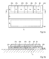
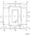
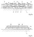
- Un transistor MOS (3) formé dans une couche de semiconducteur, et disposé sur une base isolante (1), comprenant :- une région de canal (24) d'un premier type de conductivité (P), formée dans la couche de semiconducteur;- des régions de source (22) et de drain (20) d'un second type de conductivité (N), formées dans la couche de semiconducteur et séparées par la région de canal (24);- un contact de source (28) connecté à la région de source (22);- un contact de drain (14) connecté à la région de drain (20);- une électrode de commande (27) formée sur la région de canal (24) et séparée de celle-ci par une couche isolante (26), la région de canal (24) et l'électrode de commande (27) s'étendant jusqu'à des bords opposés de la couche de semiconducteur;- une région inférieure (23) du premier type de conductivité (P), formée dans la couche de semiconducteur, au-dessous de la région de source (22), cette région inférieure (23) étant contiguë à la couche de canal (24) et étant plus fortement dopée que la couche de canal (24);caractérisé en ce que- une région d'arrêt de tranche (21) du premier type de conductivité (P) est formée dans la couche de semiconducteur et est disposée de façon contiguë à la région de source (22), à la région inférieure (23) et à la surface de la couche de semiconducteur,- et en ce que la région d'arrêt de tranche (21) et la région inférieure (23) séparent complètement la région de source (22) de la base (1) et des tranches de la couche de semiconducteur.
- Un transistor MOS selon la revendication 1, caractérisé en ce que la région d'arrêt de tranche (21) est plus fortement dopée que la région inférieure (23).
- Un transistor MOS selon la revendication 1 ou 2, caractérisé en ce que le contact de source (28) est connecté à la région d'arrêt de tranche (21).
- Un transistor selon l'une quelconque des revendications précédentes, caractérisé en ce que la région inférieure (23) est dopée avec une dose de dopage d'au moins 2-10¹² cm⁻².
Applications Claiming Priority (2)
| Application Number | Priority Date | Filing Date | Title |
|---|---|---|---|
| SE8703269A SE461490B (sv) | 1987-08-24 | 1987-08-24 | Mos-transistor utbildad paa ett isolerande underlag |
| SE8703269 | 1987-08-24 |
Publications (2)
| Publication Number | Publication Date |
|---|---|
| EP0304811A1 EP0304811A1 (fr) | 1989-03-01 |
| EP0304811B1 true EP0304811B1 (fr) | 1993-05-26 |
Family
ID=20369361
Family Applications (1)
| Application Number | Title | Priority Date | Filing Date |
|---|---|---|---|
| EP88113464A Expired - Lifetime EP0304811B1 (fr) | 1987-08-24 | 1988-08-19 | Transistor MOS |
Country Status (5)
| Country | Link |
|---|---|
| US (1) | US4969023A (fr) |
| EP (1) | EP0304811B1 (fr) |
| JP (1) | JPS6468970A (fr) |
| DE (1) | DE3881304T2 (fr) |
| SE (1) | SE461490B (fr) |
Families Citing this family (33)
| Publication number | Priority date | Publication date | Assignee | Title |
|---|---|---|---|---|
| US5144390A (en) * | 1988-09-02 | 1992-09-01 | Texas Instruments Incorporated | Silicon-on insulator transistor with internal body node to source node connection |
| JP2507567B2 (ja) * | 1988-11-25 | 1996-06-12 | 三菱電機株式会社 | 絶縁体基板上の半導体層に形成されたmos型電界効果トランジスタ |
| US5160989A (en) * | 1989-06-13 | 1992-11-03 | Texas Instruments Incorporated | Extended body contact for semiconductor over insulator transistor |
| FR2648623B1 (fr) * | 1989-06-19 | 1994-07-08 | France Etat | Structure de transistor mos sur isolant avec prise de caisson reliee a la source et procede de fabrication |
| US5316960A (en) * | 1989-07-11 | 1994-05-31 | Ricoh Company, Ltd. | C-MOS thin film transistor device manufacturing method |
| US5060035A (en) * | 1989-07-13 | 1991-10-22 | Mitsubishi Denki Kabushiki Kaisha | Silicon-on-insulator metal oxide semiconductor device having conductive sidewall structure |
| US5264720A (en) * | 1989-09-22 | 1993-11-23 | Nippondenso Co., Ltd. | High withstanding voltage transistor |
| JP2994670B2 (ja) * | 1989-12-02 | 1999-12-27 | 忠弘 大見 | 半導体装置及びその製造方法 |
| US5240865A (en) * | 1990-07-30 | 1993-08-31 | Texas Instruments Incorporated | Method of forming a thyristor on an SOI substrate |
| US5172208A (en) * | 1990-07-30 | 1992-12-15 | Texas Instruments Incorporated | Thyristor |
| TW214603B (en) * | 1992-05-13 | 1993-10-11 | Seiko Electron Co Ltd | Semiconductor device |
| KR940022907A (ko) * | 1993-03-31 | 1994-10-21 | 이헌조 | 비대칭 엘디디(ldd) 접합 박막트랜지스터 |
| US5773864A (en) * | 1995-04-28 | 1998-06-30 | National Semiconductor Corporation | CMOS interface circuit formed in silicon-on-insulator substrate |
| JPH09102609A (ja) * | 1995-08-03 | 1997-04-15 | Seiko Instr Inc | 半導体装置 |
| KR20000003758A (ko) * | 1998-06-29 | 2000-01-25 | 김영환 | 박막 트랜지스터 액정표시소자 |
| US6452233B1 (en) * | 1999-03-23 | 2002-09-17 | Citizen Watch Co., Ltd. | SOI device having a leakage stopping layer |
| JP2002261292A (ja) * | 2000-12-26 | 2002-09-13 | Toshiba Corp | 半導体装置及びその製造方法 |
| JP3845272B2 (ja) * | 2001-06-19 | 2006-11-15 | シャープ株式会社 | Sram及びその製造方法 |
| JP2003031811A (ja) | 2001-07-13 | 2003-01-31 | Mitsubishi Heavy Ind Ltd | トランジスタ及び半導体装置 |
| EP1519421A1 (fr) | 2003-09-25 | 2005-03-30 | Interuniversitair Microelektronica Centrum Vzw | Dispositif semiconducteur à une grille multiple et son procédé de fabrication |
| EP1498958B1 (fr) * | 2003-07-18 | 2014-10-15 | Imec | Procédé de fabrication d'un dispositif semiconducteur à une grille multiple |
| TWI463526B (zh) * | 2004-06-24 | 2014-12-01 | Ibm | 改良具應力矽之cmos元件的方法及以該方法製備而成的元件 |
| US7655511B2 (en) | 2005-11-03 | 2010-02-02 | International Business Machines Corporation | Gate electrode stress control for finFET performance enhancement |
| US7635620B2 (en) | 2006-01-10 | 2009-12-22 | International Business Machines Corporation | Semiconductor device structure having enhanced performance FET device |
| US20070158743A1 (en) * | 2006-01-11 | 2007-07-12 | International Business Machines Corporation | Thin silicon single diffusion field effect transistor for enhanced drive performance with stress film liners |
| US7790540B2 (en) | 2006-08-25 | 2010-09-07 | International Business Machines Corporation | Structure and method to use low k stress liner to reduce parasitic capacitance |
| KR101312259B1 (ko) * | 2007-02-09 | 2013-09-25 | 삼성전자주식회사 | 박막 트랜지스터 및 그 제조방법 |
| US8115254B2 (en) | 2007-09-25 | 2012-02-14 | International Business Machines Corporation | Semiconductor-on-insulator structures including a trench containing an insulator stressor plug and method of fabricating same |
| US8492846B2 (en) | 2007-11-15 | 2013-07-23 | International Business Machines Corporation | Stress-generating shallow trench isolation structure having dual composition |
| US8598006B2 (en) | 2010-03-16 | 2013-12-03 | International Business Machines Corporation | Strain preserving ion implantation methods |
| JP2012256928A (ja) * | 2012-08-15 | 2012-12-27 | Mitsubishi Heavy Ind Ltd | トランジスタ及び半導体装置 |
| JP2015035617A (ja) * | 2014-10-15 | 2015-02-19 | 三菱重工業株式会社 | トランジスタ及び半導体装置 |
| JP6263162B2 (ja) * | 2015-12-21 | 2018-01-17 | 三菱重工業株式会社 | トランジスタ |
Family Cites Families (10)
| Publication number | Priority date | Publication date | Assignee | Title |
|---|---|---|---|---|
| US3958266A (en) * | 1974-04-19 | 1976-05-18 | Rca Corporation | Deep depletion insulated gate field effect transistors |
| JPS5534582B2 (fr) * | 1974-06-24 | 1980-09-08 | ||
| JPS51147186A (en) * | 1975-06-12 | 1976-12-17 | Fujitsu Ltd | Semiconductor device |
| JPS5727069A (en) * | 1980-07-25 | 1982-02-13 | Toshiba Corp | Mos type simiconductor device |
| JPS57190362A (en) * | 1981-05-19 | 1982-11-22 | Nec Corp | Semiconductor device |
| JPS5898969A (ja) * | 1981-12-09 | 1983-06-13 | Nec Corp | 半導体装置 |
| JPS6115369A (ja) * | 1984-07-02 | 1986-01-23 | Nippon Telegr & Teleph Corp <Ntt> | 半導体装置及びその製造方法 |
| JPH0680830B2 (ja) * | 1985-04-08 | 1994-10-12 | 株式会社日立製作所 | 半導体装置 |
| JPH0682840B2 (ja) * | 1985-09-25 | 1994-10-19 | 日本電信電話株式会社 | Mos形半導体装置 |
| US4797721A (en) * | 1987-04-13 | 1989-01-10 | General Electric Company | Radiation hardened semiconductor device and method of making the same |
-
1987
- 1987-08-24 SE SE8703269A patent/SE461490B/sv not_active IP Right Cessation
-
1988
- 1988-08-19 EP EP88113464A patent/EP0304811B1/fr not_active Expired - Lifetime
- 1988-08-19 DE DE88113464T patent/DE3881304T2/de not_active Expired - Fee Related
- 1988-08-23 JP JP63207493A patent/JPS6468970A/ja active Pending
- 1988-08-23 US US07/235,075 patent/US4969023A/en not_active Expired - Fee Related
Also Published As
| Publication number | Publication date |
|---|---|
| JPS6468970A (en) | 1989-03-15 |
| DE3881304D1 (de) | 1993-07-01 |
| EP0304811A1 (fr) | 1989-03-01 |
| DE3881304T2 (de) | 1993-12-16 |
| SE8703269L (sv) | 1989-02-25 |
| SE8703269D0 (sv) | 1987-08-24 |
| US4969023A (en) | 1990-11-06 |
| SE461490B (sv) | 1990-02-19 |
Similar Documents
| Publication | Publication Date | Title |
|---|---|---|
| EP0304811B1 (fr) | Transistor MOS | |
| EP0110313B1 (fr) | Dispositif de circuit intégré semi-conducteur et procédé de fabrication | |
| US6060750A (en) | Semiconductor device having SOI-MOSFET | |
| US4734752A (en) | Electrostatic discharge protection device for CMOS integrated circuit outputs | |
| US5321287A (en) | Semiconductor device wherein n-channel MOSFET, p-channel MOSFET and nonvolatile memory cell are formed in one chip | |
| KR100780967B1 (ko) | 고전압용 쇼트키 다이오드 구조체 | |
| US4908682A (en) | Power MOSFET having a current sensing element of high accuracy | |
| EP0458570A1 (fr) | Diode et dispositif à semiconducteur avec une telle diode | |
| JPS6237545B2 (fr) | ||
| US4631562A (en) | Zener diode structure | |
| US5838033A (en) | Integrated circuit with gate conductor defined resistor | |
| US5990520A (en) | Method for fabricating a high performance vertical bipolar NPN or PNP transistor having low base resistance in a standard CMOS process | |
| JP2800702B2 (ja) | 半導体装置 | |
| EP0031238B1 (fr) | Dispositif semiconducteur à mémoire | |
| JP2814079B2 (ja) | 半導体集積回路とその製造方法 | |
| US4041519A (en) | Low transient effect switching device and method | |
| EP0220500B1 (fr) | Dispositif semi-conducteur à capacité de charge diminuée et son procédé de fabrication | |
| US4864380A (en) | Edgeless CMOS device | |
| EP0263287A2 (fr) | Fabrication d'un capaciteur dans un circuit intégré | |
| EP0399454B1 (fr) | Dispositif semi-conducteur monolithique comprenant des structures ccd, bipolaires et mos | |
| JP2864576B2 (ja) | 半導体装置 | |
| US4918498A (en) | Edgeless semiconductor device | |
| JPH0440865B2 (fr) | ||
| KR900002886B1 (ko) | 반도체 기억장치 | |
| US5122855A (en) | Semiconductor device with latch-up prevention structure |
Legal Events
| Date | Code | Title | Description |
|---|---|---|---|
| PUAI | Public reference made under article 153(3) epc to a published international application that has entered the european phase |
Free format text: ORIGINAL CODE: 0009012 |
|
| AK | Designated contracting states |
Kind code of ref document: A1 Designated state(s): CH DE FR GB IT LI |
|
| 17P | Request for examination filed |
Effective date: 19890619 |
|
| 17Q | First examination report despatched |
Effective date: 19910828 |
|
| GRAA | (expected) grant |
Free format text: ORIGINAL CODE: 0009210 |
|
| AK | Designated contracting states |
Kind code of ref document: B1 Designated state(s): CH DE FR GB IT LI |
|
| REF | Corresponds to: |
Ref document number: 3881304 Country of ref document: DE Date of ref document: 19930701 |
|
| ET | Fr: translation filed | ||
| ITF | It: translation for a ep patent filed |
Owner name: JACOBACCI CASETTA & PERANI S.P.A. |
|
| PLBE | No opposition filed within time limit |
Free format text: ORIGINAL CODE: 0009261 |
|
| STAA | Information on the status of an ep patent application or granted ep patent |
Free format text: STATUS: NO OPPOSITION FILED WITHIN TIME LIMIT |
|
| 26N | No opposition filed | ||
| PGFP | Annual fee paid to national office [announced via postgrant information from national office to epo] |
Ref country code: GB Payment date: 19960812 Year of fee payment: 9 |
|
| PGFP | Annual fee paid to national office [announced via postgrant information from national office to epo] |
Ref country code: CH Payment date: 19960905 Year of fee payment: 9 |
|
| PG25 | Lapsed in a contracting state [announced via postgrant information from national office to epo] |
Ref country code: GB Free format text: LAPSE BECAUSE OF NON-PAYMENT OF DUE FEES Effective date: 19970819 |
|
| PG25 | Lapsed in a contracting state [announced via postgrant information from national office to epo] |
Ref country code: LI Free format text: LAPSE BECAUSE OF NON-PAYMENT OF DUE FEES Effective date: 19970831 Ref country code: CH Free format text: LAPSE BECAUSE OF NON-PAYMENT OF DUE FEES Effective date: 19970831 |
|
| GBPC | Gb: european patent ceased through non-payment of renewal fee |
Effective date: 19970819 |
|
| REG | Reference to a national code |
Ref country code: CH Ref legal event code: PL |
|
| PGFP | Annual fee paid to national office [announced via postgrant information from national office to epo] |
Ref country code: FR Payment date: 19980814 Year of fee payment: 11 |
|
| PGFP | Annual fee paid to national office [announced via postgrant information from national office to epo] |
Ref country code: DE Payment date: 19980831 Year of fee payment: 11 |
|
| PG25 | Lapsed in a contracting state [announced via postgrant information from national office to epo] |
Ref country code: FR Free format text: LAPSE BECAUSE OF NON-PAYMENT OF DUE FEES Effective date: 20000428 |
|
| PG25 | Lapsed in a contracting state [announced via postgrant information from national office to epo] |
Ref country code: DE Free format text: LAPSE BECAUSE OF NON-PAYMENT OF DUE FEES Effective date: 20000601 |
|
| REG | Reference to a national code |
Ref country code: FR Ref legal event code: ST |
|
| PG25 | Lapsed in a contracting state [announced via postgrant information from national office to epo] |
Ref country code: IT Free format text: LAPSE BECAUSE OF NON-PAYMENT OF DUE FEES;WARNING: LAPSES OF ITALIAN PATENTS WITH EFFECTIVE DATE BEFORE 2007 MAY HAVE OCCURRED AT ANY TIME BEFORE 2007. THE CORRECT EFFECTIVE DATE MAY BE DIFFERENT FROM THE ONE RECORDED. Effective date: 20050819 |