EP0294363B1 - Méthode et dispositif pour positionner et aligner la structure d'image d'un masque sur un substrat - Google Patents
Méthode et dispositif pour positionner et aligner la structure d'image d'un masque sur un substrat Download PDFInfo
- Publication number
- EP0294363B1 EP0294363B1 EP88890133A EP88890133A EP0294363B1 EP 0294363 B1 EP0294363 B1 EP 0294363B1 EP 88890133 A EP88890133 A EP 88890133A EP 88890133 A EP88890133 A EP 88890133A EP 0294363 B1 EP0294363 B1 EP 0294363B1
- Authority
- EP
- European Patent Office
- Prior art keywords
- markings
- reference block
- mask
- wafer
- image
- Prior art date
- Legal status (The legal status is an assumption and is not a legal conclusion. Google has not performed a legal analysis and makes no representation as to the accuracy of the status listed.)
- Expired - Lifetime
Links
Images


Classifications
-
- B—PERFORMING OPERATIONS; TRANSPORTING
- B82—NANOTECHNOLOGY
- B82Y—SPECIFIC USES OR APPLICATIONS OF NANOSTRUCTURES; MEASUREMENT OR ANALYSIS OF NANOSTRUCTURES; MANUFACTURE OR TREATMENT OF NANOSTRUCTURES
- B82Y10/00—Nanotechnology for information processing, storage or transmission, e.g. quantum computing or single electron logic
-
- H—ELECTRICITY
- H01—ELECTRIC ELEMENTS
- H01J—ELECTRIC DISCHARGE TUBES OR DISCHARGE LAMPS
- H01J37/00—Discharge tubes with provision for introducing objects or material to be exposed to the discharge, e.g. for the purpose of examination or processing thereof
- H01J37/30—Electron-beam or ion-beam tubes for localised treatment of objects
- H01J37/317—Electron-beam or ion-beam tubes for localised treatment of objects for changing properties of the objects or for applying thin layers thereon, e.g. for ion implantation
- H01J37/3174—Particle-beam lithography, e.g. electron beam lithography
-
- B—PERFORMING OPERATIONS; TRANSPORTING
- B82—NANOTECHNOLOGY
- B82Y—SPECIFIC USES OR APPLICATIONS OF NANOSTRUCTURES; MEASUREMENT OR ANALYSIS OF NANOSTRUCTURES; MANUFACTURE OR TREATMENT OF NANOSTRUCTURES
- B82Y40/00—Manufacture or treatment of nanostructures
-
- H—ELECTRICITY
- H01—ELECTRIC ELEMENTS
- H01J—ELECTRIC DISCHARGE TUBES OR DISCHARGE LAMPS
- H01J2237/00—Discharge tubes exposing object to beam, e.g. for analysis treatment, etching, imaging
- H01J2237/15—Means for deflecting or directing discharge
- H01J2237/151—Electrostatic means
- H01J2237/1516—Multipoles
-
- H—ELECTRICITY
- H01—ELECTRIC ELEMENTS
- H01J—ELECTRIC DISCHARGE TUBES OR DISCHARGE LAMPS
- H01J2237/00—Discharge tubes exposing object to beam, e.g. for analysis treatment, etching, imaging
- H01J2237/30—Electron or ion beam tubes for processing objects
- H01J2237/304—Controlling tubes
- H01J2237/30433—System calibration
- H01J2237/30438—Registration
-
- H—ELECTRICITY
- H01—ELECTRIC ELEMENTS
- H01J—ELECTRIC DISCHARGE TUBES OR DISCHARGE LAMPS
- H01J2237/00—Discharge tubes exposing object to beam, e.g. for analysis treatment, etching, imaging
- H01J2237/30—Electron or ion beam tubes for processing objects
- H01J2237/317—Processing objects on a microscale
- H01J2237/3175—Lithography
- H01J2237/31752—Lithography using particular beams or near-field effects, e.g. STM-like techniques
- H01J2237/31755—Lithography using particular beams or near-field effects, e.g. STM-like techniques using ion beams
-
- H—ELECTRICITY
- H01—ELECTRIC ELEMENTS
- H01J—ELECTRIC DISCHARGE TUBES OR DISCHARGE LAMPS
- H01J2237/00—Discharge tubes exposing object to beam, e.g. for analysis treatment, etching, imaging
- H01J2237/30—Electron or ion beam tubes for processing objects
- H01J2237/317—Processing objects on a microscale
- H01J2237/3175—Lithography
- H01J2237/31776—Shaped beam
Definitions
- the invention relates to an arrangement for ion projection lithography in accordance with the preamble of claim 1.
- the preferred area of application is scaling down or 1: 1 ion projection lithography.
- Ion Projection Lithography "made it known to mark in a mask to image a carrier also provided with markings and to bring the images of the mask markings in coincidence with the carrier markings. Ion beams that have passed through the markings on the mask are electrostatically passed over the Carrier markings are scanned and the secondary beams emanating from the carrier markings are fed to detectors. For the alignment in X, Y, ⁇ and the scale 8 detectors are provided, namely two for each direction between the projection lens and the carrier, which is formed here by the wafer. The markers and detectors are arranged so that the measurements are decoupled for each direction. An electronic feedback system on the octopole, the solenoid and the projection lens aligns the beam passing through the mask marks with the center lines of the carrier marks.
- the object of the invention is to be able to observe any changes in the imaging system, in particular also during the imaging, that is to say “on line”, such as can occur as a result of vibrations or through drift of the lens voltages supplied by power supply units, and to carry out the corresponding corrections.
- the carrier provided with the markings is a reference block arranged in a predetermined position relative to the wafer, but spatially separate from the wafer, preferably parallel to the wafer, in the beam direction in front of the wafer, which has an opening which corresponds to the size of the mask image formed on the wafer, so that the markings are arranged outside the beam path of the ion projection device which forms the image on the wafer, and the detectors are arranged to receive the secondary radiation emitted by the markings on the reference block are and that the device for scale correction in the 1: 1 shadow projection is designed as a mechanical device for changing the height of the wafer.
- the arrangement of the reference block provides shadowing against the detection of secondary electrons which result from the ion beams impinging on the wafer, so that the detectors are not influenced by the wafer, which could influence the display and thus the correction.
- an optical alignment device being used to determine deviations in the positional correspondence of the markings on the reference block and on the wafer is provided.
- This optical device can be designed, for example, as described in SPIE Vol.632 "Electron-Beam, X-Ray, & Ion Beam Techniques for Submicrometer Lithographies V (1986) pp. 146-155 by BSFay et al".
- the optical device provided for determining deviations in the positional correspondence of the line markings can be coupled to a control device for the movement of the table on which the wafer is fastened, with signals from the optical device, the control device for the table movement are feedable.
- the detectors for the secondary beams emanating from the markings on the reference block can be provided in a number that can be divided by two, two pairs of detectors for controlling the multipole, one pair, preferably in combination with one of the pairs for controlling the multipole , for controlling the device for generating a magnetic rotating field and a further pair for controlling a lens upstream of the reference block (projection lens) are provided either in the sense of enlarging or reducing the image.
- Each pair of detectors is assigned a straight-line marking on the reference block, two of the markings being arranged in alignment with one another on the reference block, a third marking being arranged at an angle, preferably at a right angle to the two aligning markings, and a fourth marking is arranged parallel to the third, but offset laterally to this on the reference block.
- the third marking which is at an angle to these markings, is arranged in the line of symmetry between the two marks which are aligned with one another.
- the straight-line markings are formed by a metallic groove which is preferably V-shaped in cross section.
- the two detectors are arranged on different sides of the respective marking outside the sphere of influence of particles originating from other markings, so that it is ensured that only particles of the marking respectively assigned to a pair of detectors on the reference block are detected by this pair of detectors .
- the table can be assigned adjusting devices for adjustment in two mutually perpendicular directions in a plane perpendicular to the optical axis of the ion projection device, further adjusting devices for rotating the table about the optical axis and adjusting devices for the height adjustment of the table.
- the correction movements controlled by the interferometer are like this directed that the relative position between the reference block and table set before exposure via the optical alignment system is maintained.
- a turntable In order to rotate the table and thus the image of the mask structure about the optical axis, a turntable can be provided which carries a coordinate table (movement in the X and Y directions) or is arranged thereon.
- the turntable is operated by a motor which is controlled by the control device for the alignment in the X and Y directions and for the angular adjustment ⁇ .
- the rotation of the image of the mask structure about the optical axis can, however, also be accomplished by rotating the mask about the optical axis.
- the mask is driven by a motor via a gearbox, the motor being controlled by the control device for the alignment in the X and Y directions and for the angular adjustment ⁇ .
- Another embodiment variant according to the invention is characterized in that the optical device for determining deviations in the positional correspondence of the line markings is not coupled to the actuating devices for the table, but rather to the control device for the multipole and the axial magnetic field.
- This arrangement allows the ion-optical beam path to be influenced as a function of the deviation of the positional correspondence of the line markings on the reference block and on the wafer.
- the procedure is such that the table is brought into a position in which the markings on the wafer are only less than a predetermined dimension, for example less than 1 »m, from the target position relative to the further markings of the Reference block deviate (rough alignment), after which the interferometer is activated, ie acts on the adjustment device of the table and is kept at least until the end of the exposure in the active state and that after activation of the interferometer, but before the exposure, which with the optical Alignment system detected deviations in the positional correspondence of the further markings provided on the reference block with respect to the markings assigned to them on the wafer are corrected ion-optically, namely according to a (functionally) predetermined relationship between the optically determined deviation and the action variables on the ion projection device for correcting this deviation, after which the exposure then takes place.
- a predetermined dimension for example less than 1 »m
- the table is initially roughly aligned with the desired chip position relative to the reference block, after which the table position is held relative to the reference block by activating the interferometer and the optically determined deviation between chip and reference block is corrected ion-optically. It is essential that the functional relationship (calibration curve) between the optically determined deviation and the action necessary to correct it on the ion projection device (application of the multipole to correct the beam in the x and y direction, size of the axial magnetic field, and voltage) the projection lens).
- the detectors for the secondary radiation are reactivated, as a result of which the markings on the mask are brought back into line with the markings on the reference block, the interferometer being inactive to obtain a new table position relative to the reference block for the purpose of exposing another chip is transferred.
- the exposure of a chip can also take place in stages, that is to say that an exposure is followed by at least one further exposure in order to expose one and the same chip using the same mask in at least one further stage, the beam position being opposite again between two successive exposures the reference block is corrected.
- the procedure is such that, between two successive exposures, the imaging of the markings of the mask is again aligned with the markings of the reference block via the secondary radiation detectors, after which the detectors are put into the inactive state and the ion-optical device is now dependent on the optically determined deviation the additional markings of the reference block are corrected by the assigned markings on the wafer, after which a further exposure takes place.
- the ion-optical correction can also be carried out “on line” during the exposure — in accordance with the calibration curve — with the optically determined deviation of the additional markings on the reference block from the markings on the wafer.
- both the stabilization of the image of the mask with respect to the reference block is maintained during the chip exposure process, and the table position with respect to the reference block is checked and compensated for deviations thereof.
- This is accomplished in a further embodiment of the invention in that only the rays passing through the mask markings are subjected to the influence of a time-variable field and thus over an area of the reference block containing the markings assigned to the maskings, preferably at a constant speed.
- the detector delivers a maximum signal to which a certain instantaneous value of the time-varying deflection voltage for the reference beams is assigned, that this instantaneous value is compared with a nominal voltage value that corresponds to the maximum detector signal when the signal is stabilized , ie image of the mask structure that does not move relative to the reference block, and that the difference between the instantaneous value of the deflection voltage and the target voltage value by influencing the ion-optical imaging systems is compensated.
- deflection units for example octopoles, connected as electrical dipoles
- additional deflection units do not act on the rays originating from the actual mask structures.
- the deflection of the rays passing through the mask markings can be achieved, for example, with a sawtooth-shaped voltage which is applied to the octopoles connected as electrical dipoles. If the deflection speed is not constant, its time dependency must be known exactly.
- a maximum signal is always obtained from a reference mark on the reference block when the time-varying voltage at the corresponding "reference octopole" reaches a certain fixed value, Uo.
- a change in the voltage value by ⁇ Uo at which the maximum reference mark signal occurs indicates a drift of the reference beam, i.e. the actual image and the reference beams, e.g. a distance ⁇ x.
- the drifting of the beam can be determined either by a time measurement or a voltage measurement.
- the image is stabilized with the aid of the ion-optical correction units (multipole, axial magnetic field, voltage change of the projection lens) so that the detector signal originating from the reference marks is always at a maximum at the same reference octopole voltage Uo or always after the same time interval ⁇ to.
- the ion-optical correction units multipole, axial magnetic field, voltage change of the projection lens
- Shutters of different types can be provided in different configurations in the ion projection device and in different designs.
- All of the alignment measures described above are suitable for 1: 1 ion projection lithography or for reducing ion projection lithography.
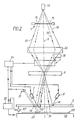
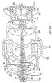
- 1 denotes a mask which is arranged in the beam path of rays coming from an ion source 22.
- the mask 1 is provided with a structure 32 (FIG. 5) which is to be imaged on a substrate 29 by means of the ion projection device.
- the mask structure 32 must be imaged on the substrate 29 in such a way that a predetermined relative position between the image of the mark structure 32 and an image already present on the substrate 29 is achieved.
- the mask 1 is provided with markings 11-13 (which are exaggerated in the drawing). These markings 11-13 are imaged on a carrier likewise provided with markings 16-18, which serves as reference block 2.
- the images of the markings 11-13 of mask 1 on reference block 2 are coincident with the existing ones on reference block 2. brought corresponding markings 16-18.
- An electrostatic multi-esp. Octopole 3, which can be influenced by a control device 34, and a device 4 for generating an axial magnetic field about the optical axis are arranged in the beam path between the mask 1 and the reference block 2.
- reference block 2 is arranged parallel to substrate (wafer) 29.
- the reference block 2 has an opening 31.
- the size of this opening 31 is designed in accordance with the image of the structure on the mask 1 that is formed on the wafer (substrate) 29. In this way, the markings 16-18 on the reference block 2 lie outside the beam path 36 of the ion projection device producing the image on the wafer 29.
- Detectors 7-10 are provided for the secondary radiation emanating from the markings 16-18 on the reference block 2, the arrangement and function of which will be explained in more detail below.
- the secondary radiation originates from the reference beams 33 passing through the mask markings 11-13 and striking the reference block 2.
- the signals from the detectors 7-10 can be fed to the control device 34 for the multi-in particular octopole 3 and the axial magnetic field.
- the arrangement of the reference block 2 has the advantage that shading of the beam is achieved and thus an influence on the detectors 7-10 by beams coming from below (from the substrate 29) is excluded.
- the reference block 2 is provided with further markings 19, which can be designed, for example, as a grating.
- markings 20 On the wafer 29 there are markings 20 corresponding to the marking 19, for example also in the form of a grating.
- an optical device 21 is provided to determine whether there are deviations in the positional correspondence from those on the reference block 2 and on the wafer 29 Markings 19 and 20 exist.
- the optical device 21 can be coupled to a control device 35 for moving the table 30 on which the wafer 29 is attached. Signals from the optical device 21 are then fed to the control device 35 for the table movement.
- the table can be a coordinate table that can be moved in two mutually perpendicular directions. The control device 35 then controls the motors for the movement of the table 30.
- the optical device 21 can also be coupled to a control device 34 for the multipole 3 and the axial magnetic field.
- the position of the projection beam 36 and also the position of the reference beam 33 are changed depending on the size of the error in the positional correspondence of the line markings 19 with the line markings 20.
- An interferometer 37 can be arranged between the reference block 2 and the table 30. When a relative movement of the table 30 with respect to the reference block 2 occurs, this interferometer supplies signals to the control device 35 for the table movement for the purpose of resetting the table 30.
- deflection units 38 for example octopoles, which are connected as an electrical dipole field, are arranged in the beam path excluding the reference beams 33.
- the reference beams 33 are continuously wobbled over the marks 16-18 of the reference block 2 during the alignment and exposure process, for example by applying a sawtooth voltage to the deflection units 38.
- the beams 36 which generate the actual image of the mask structures 32, are generated by the deflection units 38 not affected.
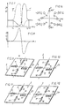
- FIG. 3 shows the - idealized - conditions that occur when the wafer table 30 is exactly aligned with the reference block 2, the optical one So device 21 does not provide a signal.
- the reference beam 33 lies exactly on the assigned reference mark of the reference block 2. The distance s covered by the reference beam is determined by the difference between the maximum and minimum voltages Umax - Umin.
- FIG. 4 shows a block diagram, for example, which shows how the ion-optical correction elements 3 and 4 both via the detectors 7-10, of which only the detector 7 is shown, for the reference marks 16-18 (for stabilizing the ion optics). as well as via the optical device 21 (for correcting displacements of the wafer 29 with respect to the reference block 2).
- the unit A always measures the voltage applied to the octopole 38 when the voltage supplied by the detector 7 is proportional to the counting rate and supplies this voltage U (Zmax) to the unit B.
- This unit compares U (Zmax) with the target voltage Uo, that is the voltage at the octopole 38 at which the reference beam 33 should sweep over the assigned reference mark on the reference block 6 when the table 30 is ideally aligned.
- the measured difference is converted into a corresponding signal for the ion-optical correction elements 3, so that the reference mark is again swept at the nominal voltage Uo.
- the optical device 21 now measures a displacement of the wafer 29 with respect to the reference block 2, a corresponding signal is transmitted to the unit C, which converts it into ion-optical correction signals with which the entire ion beam, that is to say also the portion formed by the reference beams 33 , be distracted or rotated.
- the reference beam 33 now does not sweep the assigned reference mark at Uo, but at Uo + ⁇ Uo, ⁇ Uo being clearly determined by the optical device 21.
- the signals originating from B and origin are added in the unit D and fed to the correction elements 6 for the ion beam.
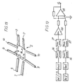
- FIG. 5 shows in detail - an electrostatic in the beam path between mask 1 and reference block 2 Multipole 3 on.
- this multipole is reproduced as an octopole.
- detectors 7 to 10 are provided which, when the markings 11-13 of the mask 1 are projected onto the reference block 2, supply a voltage which corresponds to the secondary radiation emanating from the markings 16-18 of the reference block 2.
- the detectors are provided in a number that can be divided by two. In the illustrated embodiment, a total of eight detectors are provided for the secondary radiation, two pairs 7, 8 are used to control the multipole 3, a pair 9 can control the device 4 for generating the rotating magnetic field, but it is preferable if the pair 9 in association with a pair 8 of the pairs 7, 8 provided for the control of the multipole 3 controls the device 4 for the generation of the magnetic rotating field.
- the pair of detectors 10 controls the voltage supplied to the projection lens 6 so that, depending on the change in this voltage, the image of the structures can be enlarged or reduced from the mask 1 to the reference block 2.
- the detectors can commercially available electron multiplier channels, which generate the control voltage U o depending on the detected electrons by means of the downstream electronics (Fig. 13).
- Each pair of detectors 7 to 10 is assigned a straight line marking 16 to 18 on reference block 2. The assignment is made so that two straight line markings 16 are aligned with one another on reference block 2, a third straight line marking 17 is at right angles to the two aligned marks 16, and finally a fourth rectilinear mark 18 is parallel to the third Marking 17, however laterally offset to this, arranged on the reference block 2.
- the marking 17 lies in the line of symmetry 29 between the mutually aligned markings 16, so that if the marking 18 lying outside the line of symmetry 29 does not match the associated image of the marking 13 of the mask 1, the correspondence can be achieved simply by changing the scale of the figure (FIG. 11, 12).
- the straight-line markings 16-18 on the reference block 2 are designed as a groove with a V cross-section.
- FIGS. 7 and 8 show the processes that occur when a beam is guided in the X direction via a marking 16 designed as a V-shaped groove.
- the width b of the beam can be approximately 1 »m.
- the movement of the beam in the X direction is considered to be caused by electrostatic influence on the beam.
- 6 and 6 denote the detectors of the pair of detectors. At the point X1 begins with a shift of the beam in the positive X direction, the effect of the marker 17 and ends at the point X2 + b.
- the voltages generated by the detectors I and II in the course of the displacement of the ion beam, which are a measure of the secondary radiation received by the detectors, can be seen in FIG. 7, or the voltage curve for the detector II is entered in an interrupted line , and the voltage curve for the detector I in a continuous line.
- FIG. 13 shows how the voltage signals formed by the two detectors, which are assigned to a marker, for example marker 16 in FIG. 15, are converted into control voltage U o , for example for a deflection in the X direction.
- the pulses emitted by the detectors are amplified, converted into rectangular pulses by the discriminators 26, then integrated in the ratemeter 27 (for example an integrator) to form a voltage proportional to the pulse rate.
- the inverter 28 reverses the voltage thus generated, that of the a detector (detector I) is converted into its negative value, so that the operational amplifier 25 is driven with the difference between the voltages supplied by the two detectors I, II.
- the voltage U o supplied by the operational amplifier 25 is used, in accordance with the markings from which the signal originates, to control the multipole 3 to generate the magnetic rotating field or to control the projection lens 6.
- FIG. 14 shows an example of how the voltage U o is applied to an octopole so that it causes a deflection in the X direction. Since, in general, deflection is also to take place in the Y direction, namely whenever the detectors assigned to the corresponding marking (17 in FIGS. 15 and 9-12) simultaneously deliver a signal U y , the two voltages U o and U y are added vectorially via a suitable circuit. The resulting sum voltages are fed to the corresponding poles of the octopole.
- the voltage U o supplied by the operational amplifier 25 is used to generate a current in the coil 4, which causes the rotation of the projection image, and to control the projection lens 6, with which the scale correction is carried out.
- FIGS. 9 to 12 show how the projections of the markings 11 to 13 provided on the mask 1 onto the markings 16 to 18 of the reference block 2 are set up, or respectively the projections of the markings on the Mask 1 is shown with broken lines and designated as the associated slits on mask 1, the slits of mask 1 not necessarily having to be formed as a single slit, but rather a slit also being formed by a plurality of openings of mask 1 aligned with one another can be, so that then an image is created as it is designated in FIGS. 9 to 12 with 11 to 13.
- the illustration of the mark 13 of the reference block 2 comes to lie in the apex of the V-shaped groove 17 of the reference block 2.
- the only marking that generally does not coincide with the corresponding image of a marking of the mask 1 is the marking 18, which is arranged parallel to the marking 17, but shifted laterally relative to it from the line of symmetry 29.
- FIG. 12 shows that after an adjustment in the X and Y directions as well as a rotation and change in scale has already taken place, the markings 11 to 13 of the mask 1 are now displayed on the reference block 2 with the rectilinear markings 16 located there to 18 coincides, ie the projected ion image of mask 1 is correctly aligned with the reference block.
- the adjustment steps described above for reasons of clarity, however, are expediently carried out at the same time, since they are decoupled control loops.
- the two detectors 7 to 10 assigned to a straight line marking 16 to 18 on the reference block 2 lie on different sides of the respective marking, whereby it is ensured that only particles of the assigned marking are detected.
- FIG. 16 shows a mechanical device for rotating the mask structure relative to the wafer 29 for ⁇ correction.
- the device rotates the mask 1 via a gear mechanism, which in the exemplary embodiment is designed as a gear mechanism 40, 41, the pinion 40 of which is actuated by a motor M3, which can be controlled by the control device 34 for the multipole 3 and for the angular correction. is.
- a turntable T1 is provided for performing the angular correction ⁇ (rotating the image of the mask structure).
- the rotary table T1 can be pivoted in the direction of the double arrow P by a motor M3, depending on the signal received from the control device 34.
- the rotary table T1 carries the coordinate table T, whereas, according to FIG. 18, the rotary table T1 is mounted on the coordinate table T.
- FIG. 19 shows a preferred embodiment of an ion projection lithography machine.
- the main components are sequential: the ion source 62, a solenoid 64, a mask assembly 66, the optical column 68 and the projection chamber 70.
- Ions generated in the ion source 62 are passed through a two-coil solenoid, which serves the Analyzing the ion beam and separating the desired type of ion, in the preferred embodiment these are helium ions, which are separated from other types of ions contained in the ion beam as they emerge from the ion source.
- the ion source also has an extraction electrode 74 which is at the negative potential with respect to the ion source in order to accelerate the ions generated in the ion source.
- a shield electrode 76 which is also negative with respect to the potential of the ion source, is provided by means of which an additional voltage can be applied to repel electrons and thereby prevent their inflow to the optical column.
- the extraction electrode 74 is followed by a table 78 for aligning the ion source in the X and Y directions. This table allows the entire ion source to slide to allow accurate alignment of the ion source with the axis of column 68.
- the two coils 80 and 82 of the solenoid 64 are wound opposite to each other to produce magnetic fields rotating in opposite directions which act on the ions and prevent the beam from rotating about its axis as a result of the passage of the solenoid. The solenoid also reduces the angle at which the beam strikes the mask assembly 66.
- An electrical shutter 86 which is formed by a multipole arrangement, is also located in the first coil 80 of the solenoid. The electric shutter deflects the beam from the column axis due to dipole fields that are formed in the electric shutter.
- this multipole can also generate quadrupole fields in order to regulate the magnification on the source beam in the X and Y directions, ie a plane perpendicular to the axis of the beam, and thereby correct elliptical distortions in the source.
- a vacuum isolation valve 144 is also provided in the area of the solenoid, which enables the optical column 68 to be separated from the source in order to replace or repair the source with another.
- a monitor 128 for the dose is located behind the solenoid. The outer edge of the beam strikes a known area of the monitor 78 and the induced current becomes measured. In this way, the flow of the beam through the column can be tracked and the necessary exposure time for a known resist (photoresist) can be determined.
- the beam After passing through the dose monitor 128, the beam continues on to the mask assembly 66, which has a set of mutually complementary masks 84 on a rotatable disc. Only one mask 84 is shown. Each mask is arranged in a holder 89, which enables the mask structure to rotate depending on a linear movement of a bumper 90, which is actuated by a piezoelectric transducer 92. The rotation of the mask 84 and thus also the rotation of the mask structure in the order of magnitude of ⁇ 500 microrad is controlled as a function of an alignment system for the ion beam, which will be described later.
- An exposure shutter 54 and a mask cooling cylinder 94 are arranged in front of the mask assembly 66.
- the cylinder 94 extends around the axis of the jet and is cooled by a coolant which circulates through concentric windings 96. Cylinder 94 also cools the mask by radiation. As soon as the shutter 54 is in a position in which it covers the beam with respect to the mask, it also prevents radiation cooling by the cylinder 94.
- the single lens has three electrodes.
- the first electrode 102 and the third electrode 104 are formed in one piece with a body which surrounds the column and is made of metal.
- the two electrodes are at the same potential.
- the second or center electrode 106 has different potentials that accelerate the ions.
- a pair of field control apertures 110 are disposed on each side of the center electrode 106 to cut its electric field and thereby avoid distortions that may be caused by such fields in a known manner.
- the course of the beam is changed by the single lens, so that the beam converges and forms an intersection or an image of the ion source between the single lens 112 and a second immersion lens 114 of a so-called gap lens, which in turn serves to accelerate ions and form an image to form the mask structure on the projection table 116.
- the immersion lens 114 is, in a known manner, a lens consisting of two electrodes, the two electrodes being at different potentials.
- the first electrode 118 of the immersion lens is part of the rigid body, and the second electrode 130 is carried by an insulating disk 132 at the end of the rigid enveloping body.
- the immersion lens 114 forms ion beams which travel essentially parallel to the axis of the column.
- An arrangement of such ion beams is called telecentric.
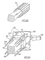
- a multipole assembly 174 Near the point where the single lens 112 forms an intersection of the ion beam, there is a multipole assembly 174, which preferably consists of two successive multipoles 120 and 122, which by applying a suitable dipole field determines the position of the beam in the X, Y plane, ie the image plane, change.
- a dipole field the strength of which is the same but opposite to the multipoles, the beam can be deflected from its original path, but remains parallel to the path.
- the size of this deflection is controlled by the alignment system for the beam, depending on signals which are generated by the alignment beams and can be, for example, ⁇ 5 »m.
- the multipoles preferably have 16 arcs, as can be seen from FIG. 22, which approximate a cylindrical surface more precisely than conventional pins and which can be used to generate any field with a regular strength, for example a dipole, quadrupole, octopole field up to a sixteen pole field.
- the higher order fields are predetermined to correct system distortions, whereas the dipole fields for the deflection are superimposed.
- the multipole assembly 174 is immediately followed by the bulkhead 124 which, in conjunction with the solenoid, serves to select ions of a desired mass.
- a multipole assembly 126 is provided for generating quadrupole fields in order to increase the relative magnification of the image in the X (M X ) and in the Y (M Y ) direction in the wafer plane to change in opposite directions. For example, if the magnification in the X direction is made smaller, the magnification in the Y direction becomes larger.
- This element is therefore used to compensate for differences in scale between the X and Y directions in order to compensate for errors which can be caused, for example, by the wafer tilting slightly in the image plane.
- the voltage of the main lens is used for the absolute adjustment of the magnification, as will be described later.
- the quadrupole assembly 126 is formed by sixteen arcs, as shown in FIG. 22.
- This assembly 126 is controlled by an alignment system for the projection beam depending on signals generated by secondary electrons that are scattered on the alignment ring (block) or on the wafer by changes in the M X and M Y values by a factor of about ⁇ 5. 10 ⁇ 4 to perform.
- the different control of the scale of M X and M Y by quadrupole fields which follow an ion projection lithography lens system can also be applied to lens combinations other than those shown in FIG. 19.
- the embodiment is arranged immediately before the beam hits the wafer, an alignment beam scanner and a detector system 136 which serves to display the position of the image formed on the wafer and to generate a signal for corrective effects of the optical elements in accordance with the alignment error is detected to initiate.
- the partial beams 148 are separated from the main field 150 in the scanner system 136 in that the partial beams pass through the outside of an insulating part 152, whereas the main field 150 runs through the center of the insulating part 152.
- the partial beams are scanned separately from the main field by using dipole fields that are generated on the scanner plate 154.
- the partial beams are scanned on a wafer 138 via reference marks 156. Scattered electrons, which are reflected back from the point of impact of the partial beams on the marks, are detected by a detector 158, which can be designed as a channeltron or electronic multiplier.
- the signals from the detectors are used to detect the position of the main field 150 on the wafer 138.
- correction fields are applied by the ion-optical elements or the rotation of the field is adjusted by rotating the mask 84.
- the position of the ring (block) with respect to the wafer can be indicated by an interferometric method, and the positioning of the main field in this case can only be made depending on the alignment marks on the ring (block).
- the structures can be applied to the wafer without there being any alignment marks on the wafer, and the wafer can simply be moved from one position to another in order to repeatedly apply structures to the wafer after a so-called "blind stepping" -Process. If the position of the alignment block is accurate is determined, the alignment block can also be used when measuring system distortions, the system operating as a measuring system.
- the wafer 138 is placed on a table 140 which allows precise movements in the X and Y directions (in the wafer plane) and in the Z direction (along the optical axis), so that the wafer moves from one position to another can be moved step by step and image repetitions can be made at different locations on the wafer. Furthermore, the position of the wafer can also be adjusted along the optical axis.
- FIG. 23 The electrical supply of the embodiment of an ion-optical lithography device shown in FIG. 19 can be seen from FIG. 23 in the form of a block diagram.
- the source 62 is kept at a positive potential with respect to the extraction electrode 78 by means of a voltage source 176, with which the acceleration potential of the extracted ions can be changed between, for example, 0 to 10 kv.
- the shield electrode 76 is connected to a voltage source 178 which holds the shield electrode 76 at a negative potential with respect to the source to repel electrons.
- a first voltage source 180 applies a negative potential to the center electrode 106 of the single lens 112 with respect to the first electrode 102 and the third electrode 104 of the single lens. This lens does not affect the net energy of the ions.
- the first electrode 102 and the third electrode 104 of the single lens and the first electrode of the immersion lens 134 are integral components of the rigid envelope body of the ion column and receive a positive potential from a second voltage supply 182.
- the immersion lens is supplied with voltage from the source 182, the negative connection of the voltage source 182 is connected to the second electrode 130 of the immersion lens, the second electrode 130 being separated from the column by an insulator 132.
- the immersion lens therefore accelerates the positive ions before they leave the column.
- the focal lengths of the electrostatic lens depend on the potential differences between its electrodes and therefore the magnification of an image behind the lenses can be changed.
- the magnification of the image in the image plane 116 is equal to the ratio of the focal length of the second lens to the focal length of the first lens, or the ratio of the voltage ratios on each lens, namely V1 / V2.
- the coarse magnification can be selected by selecting the voltage ratios of the first and second lenses. If the voltage ratios applied to the lenses are increased proportionally, the focal lengths also increase proportionally, but the magnification does not change. However, this adjustment can affect the distortion of the two lenses, as will be described later.
- voltage sources 180 and 182 are provided with supplementary sources 184 and 186, which are preferably controlled by computers and are dependent on signals which are generated by the alignment beams , are controlled to change the lens voltages by a few percent.
- FIG. 24 shows a block diagram of the alignment system.
- Secondary electrons that are emitted at the alignment marks 156 which can be located on the wafer and / or on the alignment block, as already mentioned, are detected by detectors 158, which are arranged above the marks.
- Signals S1 that are generated by the detectors are fed to a generator 160 for correction signals.
- the signal generator 160 also receives signals S2 from the scanner system 162 for the partial beams. These signals are decisive for the scanning position of the partial beams, which are scanned by the scanner plate 154, which is shown in FIG. 21.
- the signal generator 160 indicates a deviation in the alignment of the main field by processing the signals S1 and S2 and generates a corresponding correction signal S3, which in turn is the control element for the various image correction elements is fed in to carry out a corresponding corrective movement so that the main field comes into the correct position.
- the control devices for the correction is the control device for the multipole 164 for controlling the movement in the X and Y directions, the quadrupole 166 for scale changes M X and M Y , furthermore the supplementary voltage sources for the immersion lens 114 and the central electrode of the single lens 112 for correcting the magnification, and the control element for the device for rotating the mask (converter 172).
Claims (16)
- Agencement pour la lithographie par projection d'ions, avec un dispositif de projection d'ions et un support pourvu de repères (16 - 18), pour positionner sur une galette de silicium (29) la projection des structures (32) qui se trouvent sur un masque (1), les projections de repères (11 - 13) du masque (1) sur le support étant, aux fins d'alignement, en agissant sur un faisceau de référence, amenées en coïncidence avec les repères respectivement correspondants (16 - 18) présents sur le support, le dispositif de projection d'ions contenant, dans la marche des rayons, un pôle multiple, notamment un octopôle (3) soumis à l'action d'un dispositif de commande (34), ainsi qu'un dispositif (4) pour faire tourner l'image des structures (32) du masque autour de l'axe opto-ionique, et qu'un dispositif pour corriger l'échelle de projection, des détecteurs (7 - 10) étant prévus pour le rayonnement secondaire provenant des repères (16 - 18), à savoir notamment les électrons secondaires qui proviennent des faisceaux de référence (33) passant par les repères (11 - 13) du masque, et les signaux des détecteurs (7 - 10) pouvant être transmis au dispositif de commande (34) pour le pôle multiple, notamment l'octopôle (3), ainsi qu'au dispositif pour faire tourner l'image des structures du masque et qu'au dispositif de correction d'échelle, caractérisé en ce que le support pourvu des repères (16 - 18) est un bloc de référence (2), qui est disposé dans une position prédéterminée par rapport à la galette (29), avant la galette (29) dans la direction du faisceau, de préférence parallèlement à la galette mais en un lieu séparé de la galette (29), et qui présente une ouverture (31) qui correspond à la taille de la projection du masque obtenue sur la galette (29), de sorte que les repères (16 - 18) sont disposés en dehors de la marche des rayons du dispositif de projection d'ions produisant l'image sur la galette (29), en ce que les détecteurs (7 - 10) sont disposés de façon à recevoir le rayonnement secondaire émis par les repères (16 - 18) du bloc de référence, et en ce que le dispositif de correction d'échelle à l'échelle de projection 1 : 1 est conçu comme dispositif mécanique pour modifier la position en hauteur de la galette (29).
- Agencement selon la revendication 1, caractérisé en ce qu'afin de positionner la galette (29) par rapport au bloc de référence (2), le bloc de référence (2) est pourvu de repères supplémentaires (19), par exemple sous la forme d'un réseau de traits, et en ce que sont prévus sur la galette (29) des repères (20) correspondant aux repères supplémentaires (19) prévus sur le bloc de référence (2), un dispositif d'alignement optique (21) étant prévu pour déterminer les écarts de coïncidence de position des repères (19, 20) présents sur le bloc de référence (2) et la galette (29).
- Agencement selon la revendication 2, caractérisé en ce que le dispositif optique (21) pour déterminer les écarts de coïncidence de position des traits de repère prévus (19, 20) est couplé à un dispositif de commande (35) pour le déplacement d'une table (30) sur laquelle est fixée la galette (29), les signaux du dispositif optique (21) pouvant être transmis au dispositif (35) de commande du déplacement de la table.
- Agencement selon la revendication 3, caractérisé en ce que le dispositif optique (21) pour déterminer les écarts de coïncidence de position des traits de repère (19, 20) est couplé au dispositif de commande (34) pour le pôle multiple (3) et au dispositif pour faire tourner l'image des structures du masque.
- Agencement selon la revendication 3, caractérisé en ce qu'un interféromètre (37), notamment un interféromètre laser, est prévu pour déterminer les modifications de position de la galette (29) par rapport au bloc de référence (2), des dispositifs (35) de commande de la table (30) pouvant être asservis par l'interféromètre (37).
- Agencement selon l'une quelconque des revendications 1 à 5, caractérisé en ce que des unités de déflexion (38), par exemple des octopôles connectés en champ électrique dipolaire, sont disposées dans la marche des rayons des seuls faisceaux de référence (33).
- Agencement selon l'une quelconque des revendications 1 à 6, caractérisé en ce que le dispositif pour faire tourner l'image des structures du masque est conçu comme dispositif (4) pour produire un champ magnétique axial.
- Agencement selon l'une quelconque des revendications 1 à 6, caractérisé en ce que le dispositif pour faire tourner l'image des structures du masque est conçu comme mécanisme de transmission (40, 41) pour faire tourner le masque (1), mécanisme qui peut être actionné par un moteur (M3).
- Agencement selon l'une quelconque des revendications 1 à 6, caractérisé en ce que le dispositif pour faire tourner l'image des structures du masque est conçu comme table tournante (T1), qui porte la galette (29) et peut être actionnée par un moteur asservissable (M3).
- Agencement selon la revendication 9, caractérisé en ce que le moteur (M3) pour l'actionnement de la table tournante (T1) peut être asservi par le dispositif de commande (34) pour l'alignement dans la direction X et dans la direction Y et pour la rotation (ϑ).
- Agencement selon la revendication 9 ou 10, caractérisé en ce que la table tournante (T1) porte la table de coordonnées (T) (figure 17), ou est disposée sur la table de coordonnées (T) (figure 18).
- Procédé d'alignement en utilisant un agencement selon la revendication 3 ou selon la revendication 3 conjointement avec l'une quelconque des revendications 6 à 11, caractérisé en ce qu'en agissant sur le dispositif de projection d'ions pendant le processus d'alignement, les images des repères du masque sont maintenues en coïncidence avec les repères associés sur le bloc de référence, et les écarts optiquement déterminés de coïncidence de position des repères supplémentaires prévus sur le bloc de référence, par rapport aux repères qui leurs sont associés sur la galette, sont compensés en déplaçant en translation la table (30) par rapport au bloc de référence, et ce faisant, soit a) les erreurs de coïncidence de position entre les repères supplémentaires prévus sur le bloc de référence et les repères qui leur sont associés sur la galette sont détectées en continu pendant l'exposition et transformées en un déplacement correcteur de la table permettant de passer en dessous d'une valeur de seuil d'erreur, soit (b) la coïncidence de position entre les repères supplémentaires prévus sur le bloc de référence et les repères qui leur sont associés sur la galette est réalisée avant l'exposition au moyen du système d'alignement optique.
- Procédé d'alignement en utilisant un agencement selon la revendication 5 ou selon la revendication 5 conjointement avec l'une quelconque des revendications 6 à 11, caractérisé en ce qu'en agissant sur le dispositif de projection d'ions pendant le processus d'alignement, les images des repères du masque sont maintenues en coïncidence avec les repères associés sur le bloc de référence, la table (30) étant tout d'abord amenée dans une position dans laquelle les repères sur la galette ne diffèrent que de moins d'une valeur prédéterminée, par exemple moins de 1 »m, de leur position de consigne par rapport aux repères supplémentaires du bloc de référence qui leur sont associés, à la suite de quoi l'interféromètre est activé et maintenu à l'état actif au moins jusqu'à l'achèvement de l'exposition, et en ce qu'à la suite de l'activation de l'interféromètre, les écarts optiquement déterminés de coïncidence de position des repères supplémentaires prévus sur le bloc de référence, par rapport aux repères qui leurs sont associés sur la galette, sont corrigés de façon opto-ionique, en agissant sur le dispositif de projection d'ions, afin de corriger l'écart optiquement déterminé, conformément à une relation prédéterminée entre cet écart et les variables d'action sur le dispositif de projection d'ions, l'exposition étant effectuée à la suite de cette action.
- Procédé d'alignement selon la revendication 13, carac térisé en ce que l'exposition est suivie d'au moins une autre exposition, afin de soumettre une seule et même pastille à au moins une étape d'exposition supplémentaire en utilisant le même masque, et ce faisant, entre deux expositions successives, les projections des repères du masque sont alignées sur les repères du bloc de référence, à la suite de quoi les détecteurs sont désactivés et le dispositif opto-ionique est maintenant corrigé en fonction de l'écart optiquement déterminé des repères supplémentaires du bloc de référence par rapport aux repères associés sur la galette, à la suite de quoi une nouvelle exposition est effectuée.
- Procédé d'alignement selon la revendication 14, carac térisé en ce qu'à la suite de la désactivation du réglage du système de stabilisation pour la projection des repères du masque sur les repères associés du bloc de référence, le dispositif opto-ionique est, jusqu'à la fin de l'exposition, corrigé en fonction de l'écart optiquement déterminé des repères supplémentaires du bloc de référence par rapport aux repères sur la galette.
- Procédé d'alignement en utilisant un agencement selon la revendication 6 ou selon la revendication 6 conjointement avec l'une quelconque des revendications 7 à 11, avec fixation en position du bloc de référence par un procédé selon la revendication 12 ou 13, caractérisé en ce que les seuls faisceaux de référence sont soumis à l'influence d'un champ modifiable dans le temps et sont ainsi déplacés en va-et-vient, de préférence à vitesse constante, sur une zone du bloc de référence contenant les repères associés aux repères du masque, et ce faisant, lors du balayage d'un repère, par exemple d'un creux, le détecteur délivre un signal maximal auquel est associée une valeur momentanée déterminée de la tension de déflexion, variable dans le temps, pour les faisceaux de référence, en ce que cette valeur momentanée est comparée à une valeur de tension de consigne qui correspond au signal maximal du détecteur pour une image stabilisée des structures du masque, c'est-à-dire ne bougeant pas par rapport au bloc de référence, lorsque les faisceaux de référence balayent un repère du bloc de référence, et en ce que la différence entre la valeur momentanée de la tension de déflexion et la valeur de tension de consigne est compensée en agissant sur le système de projection opto-ionique.
Priority Applications (3)
| Application Number | Priority Date | Filing Date | Title |
|---|---|---|---|
| DE68928821T DE68928821D1 (de) | 1988-06-01 | 1989-05-26 | Ionenstrahllithographie |
| AT89109553T ATE171812T1 (de) | 1988-06-01 | 1989-05-26 | Ionenstrahllithographie |
| EP89109553A EP0344646B1 (fr) | 1988-06-01 | 1989-05-26 | Lithographie par faisceaux d'ions |
Applications Claiming Priority (2)
| Application Number | Priority Date | Filing Date | Title |
|---|---|---|---|
| AT0140487A AT393925B (de) | 1987-06-02 | 1987-06-02 | Anordnung zur durchfuehrung eines verfahrens zum positionieren der abbildung der auf einer maske befindlichen struktur auf ein substrat, und verfahren zum ausrichten von auf einer maske angeordneten markierungen auf markierungen, die auf einem traeger angeordnet sind |
| AT1404/87 | 1987-06-02 |
Publications (3)
| Publication Number | Publication Date |
|---|---|
| EP0294363A2 EP0294363A2 (fr) | 1988-12-07 |
| EP0294363A3 EP0294363A3 (fr) | 1991-04-17 |
| EP0294363B1 true EP0294363B1 (fr) | 1994-09-28 |
Family
ID=3513165
Family Applications (1)
| Application Number | Title | Priority Date | Filing Date |
|---|---|---|---|
| EP88890133A Expired - Lifetime EP0294363B1 (fr) | 1987-06-02 | 1988-06-01 | Méthode et dispositif pour positionner et aligner la structure d'image d'un masque sur un substrat |
Country Status (5)
| Country | Link |
|---|---|
| US (1) | US4967088A (fr) |
| EP (1) | EP0294363B1 (fr) |
| JP (1) | JPH07109817B2 (fr) |
| AT (2) | AT393925B (fr) |
| DE (1) | DE3851653D1 (fr) |
Families Citing this family (51)
| Publication number | Priority date | Publication date | Assignee | Title |
|---|---|---|---|---|
| ATE171812T1 (de) * | 1988-06-01 | 1998-10-15 | Ims Ionen Mikrofab Syst | Ionenstrahllithographie |
| US5168306A (en) * | 1989-04-04 | 1992-12-01 | Asahi Kogaku Kogyo Kabushiki Kaisha | Exposure apparatus |
| DE3941889A1 (de) * | 1989-12-19 | 1991-06-20 | Integrated Circuit Testing | Verfahren und vorrichtung zur potentialmessung auf leiterbahnen einer programmgesteuerten integrierten schaltung |
| JP3192500B2 (ja) * | 1992-11-19 | 2001-07-30 | 株式会社日立製作所 | 電子線描画方法および電子線描画装置 |
| US5742062A (en) * | 1995-02-13 | 1998-04-21 | Ims Mikrofabrikations Systeme Gmbh | Arrangement for masked beam lithography by means of electrically charged particles |
| JPH09320948A (ja) * | 1996-05-27 | 1997-12-12 | Nikon Corp | 基板の受け渡し方法及び露光装置 |
| US6225637B1 (en) | 1996-10-25 | 2001-05-01 | Canon Kabushiki Kaisha | Electron beam exposure apparatus |
| IL124592A (en) | 1997-05-23 | 2002-07-25 | Gersan Ets | Method of marking a gemstone or diamond |
| US6174741B1 (en) | 1997-12-19 | 2001-01-16 | Siemens Aktiengesellschaft | Method for quantifying proximity effect by measuring device performance |
| US6335534B1 (en) * | 1998-04-17 | 2002-01-01 | Kabushiki Kaisha Toshiba | Ion implantation apparatus, ion generating apparatus and semiconductor manufacturing method with ion implantation processes |
| JP2000012455A (ja) * | 1998-06-25 | 2000-01-14 | Nikon Corp | 荷電粒子線転写露光装置及び荷電粒子線転写露光装置におけるマスクと感応基板の位置合わせ方法 |
| US6989546B2 (en) * | 1998-08-19 | 2006-01-24 | Ims-Innenmikrofabrikations Systeme Gmbh | Particle multibeam lithography |
| EP0989595A3 (fr) * | 1998-09-18 | 2001-09-19 | Ims-Ionen Mikrofabrikations Systeme Gmbh | Dispositif pour le traitement d'une surface de substrat |
| US6549649B1 (en) * | 1999-03-04 | 2003-04-15 | Electroglas, Inc. | Apparatus and method for projecting an alignment image |
| US6437347B1 (en) * | 1999-04-13 | 2002-08-20 | International Business Machines Corporation | Target locking system for electron beam lithography |
| JP2001284239A (ja) * | 2000-04-03 | 2001-10-12 | Nikon Corp | 荷電粒子線露光装置、及び半導体デバイスの製造方法 |
| DE60134922D1 (de) * | 2000-08-14 | 2008-09-04 | Elith Llc | Lithographischer Apparat |
| DE10041040A1 (de) * | 2000-08-22 | 2002-03-07 | Zeiss Carl | Vorrichtung und Verfahren zur Belichtung einer strahlungsempfindlichen Schicht mittels geladener Teilchen sowie Maske hierfür |
| US6661015B2 (en) * | 2000-09-15 | 2003-12-09 | Ims-Ionen Mikrofabrikations Systeme Gmbh | Pattern lock system |
| GB2375182B (en) * | 2001-03-19 | 2004-01-14 | Ims Ionen Mikrofab Syst | Thermal control of image pattern distortions |
| DE10115915A1 (de) * | 2001-03-30 | 2002-10-02 | Zeiss Carl | Vorrichtung zur Justierung von Einrichtungen und zum Einstellen von Verstellwegen |
| DE10136387A1 (de) * | 2001-07-26 | 2003-02-13 | Zeiss Carl | Objektiv, insbesondere Objektiv für die Halbleiter-Lithographie |
| US6760641B2 (en) * | 2001-08-08 | 2004-07-06 | Asml Holding N.V. | Discrete time trajectory planner for lithography system |
| JP3984019B2 (ja) * | 2001-10-15 | 2007-09-26 | パイオニア株式会社 | 電子ビーム装置及び電子ビーム調整方法 |
| US6768125B2 (en) * | 2002-01-17 | 2004-07-27 | Ims Nanofabrication, Gmbh | Maskless particle-beam system for exposing a pattern on a substrate |
| DE10219514A1 (de) | 2002-04-30 | 2003-11-13 | Zeiss Carl Smt Ag | Beleuchtungssystem, insbesondere für die EUV-Lithographie |
| US20040120457A1 (en) * | 2002-12-20 | 2004-06-24 | University Of Massachusetts Medical Center | Scatter reducing device for imaging |
| RU2243613C1 (ru) * | 2003-07-16 | 2004-12-27 | Гурович Борис Аронович | Способ формирования объемной структуры |
| JP4199618B2 (ja) * | 2003-08-12 | 2008-12-17 | 財団法人国際科学振興財団 | 電子ビーム露光装置及び露光方法 |
| GB2408143B (en) * | 2003-10-20 | 2006-11-15 | Ims Nanofabrication Gmbh | Charged-particle multi-beam exposure apparatus |
| US7265917B2 (en) * | 2003-12-23 | 2007-09-04 | Carl Zeiss Smt Ag | Replacement apparatus for an optical element |
| GB2412232A (en) * | 2004-03-15 | 2005-09-21 | Ims Nanofabrication Gmbh | Particle-optical projection system |
| US7332729B1 (en) * | 2004-06-18 | 2008-02-19 | Novelx, Inc. | System and method for multiple electron, ion, and photon beam alignment |
| JP5505821B2 (ja) * | 2004-11-17 | 2014-05-28 | イーエムエス ナノファブリカツィオン アーゲー | 粒子ビーム露光装置のためのパターンロック装置 |
| KR100566096B1 (ko) * | 2004-11-24 | 2006-03-31 | 한국전자통신연구원 | 노광 장치 |
| US7459701B2 (en) * | 2005-06-08 | 2008-12-02 | Asml Netherlands B.V. | Stage apparatus, lithographic apparatus and device manufacturing method |
| US20080099696A1 (en) * | 2006-10-31 | 2008-05-01 | Applied Materials, Inc. | Shaped apertures in an ion implanter |
| NL2001369C2 (nl) * | 2007-03-29 | 2010-06-14 | Ims Nanofabrication Ag | Werkwijze voor maskerloze deeltjesbundelbelichting. |
| DE102008004762A1 (de) | 2008-01-16 | 2009-07-30 | Carl Zeiss Smt Ag | Projektionsbelichtungsanlage für die Mikrolithographie mit einer Messeinrichtung |
| DE102008000967B4 (de) | 2008-04-03 | 2015-04-09 | Carl Zeiss Smt Gmbh | Projektionsbelichtungsanlage für die EUV-Mikrolithographie |
| JP2010040732A (ja) * | 2008-08-05 | 2010-02-18 | Nuflare Technology Inc | 描画装置及び描画方法 |
| US8749053B2 (en) | 2009-06-23 | 2014-06-10 | Intevac, Inc. | Plasma grid implant system for use in solar cell fabrications |
| WO2011100363A1 (fr) * | 2010-02-09 | 2011-08-18 | Intevac, Inc. | Ensemble masque perforé ajustable pour une utilisation dans des fabrications de cellules solaires |
| US20120223245A1 (en) * | 2011-03-01 | 2012-09-06 | John Bennett | Electron beam source system and method |
| KR20140027298A (ko) | 2011-04-22 | 2014-03-06 | 마퍼 리쏘그라피 아이피 비.브이. | 웨이퍼와 같은 타겟의 처리를 위한 리소그래피 시스템 및 웨이퍼와 같은 타겟의 처리를 위한 리소그래피 시스템 작동 방법 |
| EP2699967B1 (fr) | 2011-04-22 | 2023-09-13 | ASML Netherlands B.V. | Détermination d'une position dans un système de lithographie à l'aide d'un substrat doté d'une marque de positionnement partiellement réfléchissante |
| JP5932023B2 (ja) | 2011-05-13 | 2016-06-08 | マッパー・リソグラフィー・アイピー・ビー.ブイ. | ターゲットの少なくとも一部を処理するためのリソグラフィシステム |
| CN106847736B (zh) | 2011-11-08 | 2020-08-11 | 因特瓦克公司 | 基板处理系统和方法 |
| EP2912521A1 (fr) | 2012-10-26 | 2015-09-02 | Mapper Lithography IP B.V. | Détermination d'une position d'un substrat de lithographie |
| MY178951A (en) | 2012-12-19 | 2020-10-23 | Intevac Inc | Grid for plasma ion implant |
| US9333733B2 (en) * | 2013-07-26 | 2016-05-10 | Varian Semiconductor Equipment Associates, Inc. | Multi-part mask for implanting workpieces |
Citations (1)
| Publication number | Priority date | Publication date | Assignee | Title |
|---|---|---|---|---|
| EP0325575A2 (fr) * | 1988-01-22 | 1989-07-26 | IMS Ionen Mikrofabrikations Systeme Gesellschaft m.b.H. | Dispositif de stabilisation d'un masque illuminé |
Family Cites Families (36)
| Publication number | Priority date | Publication date | Assignee | Title |
|---|---|---|---|---|
| NL158008B (nl) * | 1950-04-28 | Ibm | Holografisch geheugen. | |
| US2919381A (en) * | 1956-07-25 | 1959-12-29 | Farrand Optical Co Inc | Electron lens |
| NL96667C (fr) * | 1957-01-03 | |||
| US3434894A (en) * | 1965-10-06 | 1969-03-25 | Ion Physics Corp | Fabricating solid state devices by ion implantation |
| US4090077A (en) * | 1969-03-05 | 1978-05-16 | Siemens Aktiengesellschaft | Particle beam device with a deflection system and a stigmator |
| US3845312A (en) * | 1972-07-13 | 1974-10-29 | Texas Instruments Inc | Particle accelerator producing a uniformly expanded particle beam of uniform cross-sectioned density |
| JPS5145005A (ja) * | 1974-10-14 | 1976-04-17 | Kanto Itami Denki Kk | Inenoikubyohoho |
| JPS5168052A (fr) * | 1974-12-11 | 1976-06-12 | Matsushita Electric Ind Co Ltd | |
| US3928094A (en) * | 1975-01-16 | 1975-12-23 | Fairchild Camera Instr Co | Method of aligning a wafer beneath a mask and system therefor and wafer having a unique alignment pattern |
| JPS5228239A (en) * | 1975-08-29 | 1977-03-03 | Hitachi Ltd | Testing system for unit of semiconductor integrated circuit |
| DD136670A1 (de) * | 1976-02-04 | 1979-07-18 | Rudolf Sacher | Verfahren und vorrichtung zur herstellung von halbleiterstrukturen |
| DE2606169C2 (de) * | 1976-02-17 | 1983-09-01 | Polymer-Physik GmbH & Co KG, 2844 Lemförde | Elektronenaustrittsfenster für eine Elektronenstrahlquelle |
| US4085330A (en) * | 1976-07-08 | 1978-04-18 | Burroughs Corporation | Focused ion beam mask maker |
| JPS5398781A (en) * | 1976-11-25 | 1978-08-29 | Jeol Ltd | Electron ray exposure unit |
| DE2702444C3 (de) * | 1977-01-20 | 1980-10-09 | Siemens Ag, 1000 Berlin Und 8000 Muenchen | Korpuskularstrahloptisches Gerät zur Abbildung einer Maske auf ein Präparat |
| DE2739502C3 (de) * | 1977-09-02 | 1980-07-03 | Ibm Deutschland Gmbh, 7000 Stuttgart | Verfahren zur Belichtung durch Korpuskularstrahlen-Schattenwurf und Vorrichtung zur Durchführung des Verfahrens |
| US4139773A (en) * | 1977-11-04 | 1979-02-13 | Oregon Graduate Center | Method and apparatus for producing bright high resolution ion beams |
| GB1597596A (en) * | 1978-05-31 | 1981-09-09 | Funkwerk Erfurt Veb K | Manufacture of semiconductor elements |
| DE2827085C2 (de) * | 1978-06-16 | 1980-07-24 | Siemens Ag, 1000 Berlin Und 8000 Muenchen | Verfahren und Vorrichtung zur Brennweitenbestimmung langbrennweitiger elektronenoptischer Linsen |
| DE2939044A1 (de) * | 1979-09-27 | 1981-04-09 | Ibm Deutschland Gmbh, 7000 Stuttgart | Einrichtung fuer elektronenstrahllithographie |
| JPS5693318A (en) * | 1979-12-10 | 1981-07-28 | Fujitsu Ltd | Electron beam exposure device |
| US4344160A (en) * | 1980-05-02 | 1982-08-10 | The Perkin-Elmer Corporation | Automatic wafer focusing and flattening system |
| DE3033160A1 (de) * | 1980-09-03 | 1982-04-22 | Bayer Ag, 5090 Leverkusen | N-oxiamide, verfahren zu ihrer herstellung sowie ihre verwendung als fungizide |
| JPS6033708B2 (ja) * | 1980-11-28 | 1985-08-05 | 五洋建設株式会社 | アンカ−の方向表示装置 |
| DE3138896A1 (de) * | 1981-09-30 | 1983-04-14 | Siemens AG, 1000 Berlin und 8000 München | Elektronenoptisches system mit vario-formstrahl zur erzeugung und messung von mikrostrukturen |
| JPS5856332A (ja) * | 1981-09-30 | 1983-04-04 | Hitachi Ltd | マスクの欠陥修正方法 |
| JPS58106750A (ja) * | 1981-12-18 | 1983-06-25 | Toshiba Corp | フオ−カスイオンビ−ム加工方法 |
| US4408338A (en) * | 1981-12-31 | 1983-10-04 | International Business Machines Corporation | Pulsed electromagnetic radiation source having a barrier for discharged debris |
| JPS58181535A (ja) * | 1982-04-13 | 1983-10-24 | Yoshiaki Ihara | マシニングセンタ |
| JPS59200721A (ja) * | 1983-04-27 | 1984-11-14 | Toshiba Corp | シヤドウマスクの製造方法 |
| DE3370699D1 (en) * | 1983-05-25 | 1987-05-07 | Ibm Deutschland | Process for pattern transfer onto a light-sensitive layer |
| DE3375252D1 (en) * | 1983-08-11 | 1988-02-11 | Ibm Deutschland | Electron beam projection lithography |
| DE3410885A1 (de) * | 1984-03-24 | 1985-10-03 | Ibm Deutschland Gmbh, 7000 Stuttgart | Fehlerkorrigierte korpuskularstrahllithographie |
| JPH0616391B2 (ja) * | 1984-07-13 | 1994-03-02 | 株式会社日立製作所 | イオンビーム照射装置 |
| US4698236A (en) * | 1984-10-26 | 1987-10-06 | Ion Beam Systems, Inc. | Augmented carbonaceous substrate alteration |
| AT391772B (de) * | 1986-05-16 | 1990-11-26 | Ims Ionen Mikrofab Syst | Anordnung zum positionieren der abbildung der struktur einer maske auf ein substrat |
-
1987
- 1987-06-02 AT AT0140487A patent/AT393925B/de not_active IP Right Cessation
-
1988
- 1988-06-01 AT AT88890133T patent/ATE112400T1/de active
- 1988-06-01 DE DE3851653T patent/DE3851653D1/de not_active Expired - Fee Related
- 1988-06-01 EP EP88890133A patent/EP0294363B1/fr not_active Expired - Lifetime
- 1988-06-02 JP JP63136465A patent/JPH07109817B2/ja not_active Expired - Fee Related
- 1988-06-02 US US07/201,959 patent/US4967088A/en not_active Expired - Lifetime
Patent Citations (1)
| Publication number | Priority date | Publication date | Assignee | Title |
|---|---|---|---|---|
| EP0325575A2 (fr) * | 1988-01-22 | 1989-07-26 | IMS Ionen Mikrofabrikations Systeme Gesellschaft m.b.H. | Dispositif de stabilisation d'un masque illuminé |
Non-Patent Citations (1)
| Title |
|---|
| SPIE, vol. 632, Electron-Beam, X-Ray, & Ion-Beam Techniques for Submicrometer Lithographies V (1986), Seiten 146-155, B.S. Fay et al. : "Advanced X-ray alignment system" * |
Also Published As
| Publication number | Publication date |
|---|---|
| ATA140487A (de) | 1991-06-15 |
| JPS6464216A (en) | 1989-03-10 |
| AT393925B (de) | 1992-01-10 |
| EP0294363A3 (fr) | 1991-04-17 |
| EP0294363A2 (fr) | 1988-12-07 |
| JPH07109817B2 (ja) | 1995-11-22 |
| ATE112400T1 (de) | 1994-10-15 |
| DE3851653D1 (de) | 1994-11-03 |
| US4967088A (en) | 1990-10-30 |
Similar Documents
| Publication | Publication Date | Title |
|---|---|---|
| EP0294363B1 (fr) | Méthode et dispositif pour positionner et aligner la structure d'image d'un masque sur un substrat | |
| DE102018007652B4 (de) | Teilchenstrahl-System sowie Verfahren zur Stromregulierung von Einzel-Teilchenstrahlen | |
| DE102013210045B4 (de) | Schreibverfahren für einen Multistrahl geladener Teilchen und Schreibvorrichtung für einen Multistrahl geladener Teilchen | |
| DE10329383B4 (de) | Ionenstrahldetektor für Ionenimplantationsanlagen, Faraday-Behälter dafür und Verfahren zur Steuerung der Eigenschaften eines Ionenstrahls mittels des Ionenstrahldetektors | |
| DE19848070A1 (de) | Niedrigenergie-Elektronenstrahllithographie | |
| DE2702445C3 (de) | Korpuskularstrahloptisches Gerät zur verkleinernden Abbildung einer Maske auf ein zu bestrahlendes Präparat | |
| DE10312989A1 (de) | Lithographiesystem mit Strahl aus geladenen Teilchen, Lithographieverfahren, das einen Strahl aus geladenen Teilchen verwendet, Verfahren zum Steuern eines Strahls aus geladenen Teilchen, und Verfahren zur Herstellung eines Halbleiterbauteils | |
| EP1280184A2 (fr) | Système d'inspection d'optique corpusculaire pour l'imagerie d'un objet, dispositif pour la déflection des particules chargées et procédé pour son fonctionnement | |
| DE2727733C2 (de) | Elektronenstrahllithographieanordnung | |
| DE3307138A1 (de) | Belichtungssystem mit einem strahl geladener teilchen | |
| DE2647254C2 (de) | Anordnung zum Bestrahlen eines Targets mit einem Strahl geladener Teilchen und Verwendung | |
| DE2647855A1 (de) | Verfahren zum projizieren eines buendels aus geladenen partikeln | |
| DE2443121A1 (de) | Verfahren zum praezisen ausrichten eines elektronenstrahlmusters gegenueber vorbestimmten bereichen eines substrates | |
| EP0250391B1 (fr) | Dispositif de positionnement d'une structure d'image d'un masque sur un substrat | |
| DE3933317A1 (de) | Saeule zur erzeugung eines fokussierten ionenstrahls | |
| DE2512468A1 (de) | Elektronenmikroskop mit energieanalysator | |
| DE3510961C2 (fr) | ||
| EP0231164B1 (fr) | Dispositif pour appareils de projection ionique | |
| DE2726173A1 (de) | Verfahren und einrichtung zur automatischen positionierung eines werkstueckes relativ zu einem abtastfeld bzw. zu einer maske | |
| DE2805602C2 (fr) | ||
| DE4041297A1 (de) | Verfahren und vorrichtung zum waehlen der aufloesung eines ladungsteilchenstrahl-analysators | |
| EP0564438A1 (fr) | Système de formation d'images par faisceau de particules notamment système d'imagerie en optique ionique | |
| EP0440901B1 (fr) | Appareil à faisceau d'ions et procédé pour effectuer des mesures de potentiel par un faisceau d'ions | |
| DE102018215724A1 (de) | Verfahren zum Beeinflussen einer Position eines Brennflecks in einer Röntgenstrahlungsquelle eines Computertomographen und Computertomograph | |
| EP0523033A1 (fr) | Système d'imagerie en optique ionique |
Legal Events
| Date | Code | Title | Description |
|---|---|---|---|
| PUAI | Public reference made under article 153(3) epc to a published international application that has entered the european phase |
Free format text: ORIGINAL CODE: 0009012 |
|
| AK | Designated contracting states |
Kind code of ref document: A2 Designated state(s): AT BE DE FR GB IT NL SE |
|
| RAP1 | Party data changed (applicant data changed or rights of an application transferred) |
Owner name: OESTERREICHISCHE INVESTITIONSKREDIT AKTIENGESELLS Owner name: IMS IONEN MIKROFABRIKATIONS SYSTEME GESELLSCHAFT M |
|
| PUAL | Search report despatched |
Free format text: ORIGINAL CODE: 0009013 |
|
| AK | Designated contracting states |
Kind code of ref document: A3 Designated state(s): AT BE DE FR GB IT NL SE |
|
| 17P | Request for examination filed |
Effective date: 19910710 |
|
| 17Q | First examination report despatched |
Effective date: 19930215 |
|
| GRAA | (expected) grant |
Free format text: ORIGINAL CODE: 0009210 |
|
| AK | Designated contracting states |
Kind code of ref document: B1 Designated state(s): AT BE DE FR GB IT NL SE |
|
| PG25 | Lapsed in a contracting state [announced via postgrant information from national office to epo] |
Ref country code: BE Effective date: 19940928 |
|
| REF | Corresponds to: |
Ref document number: 112400 Country of ref document: AT Date of ref document: 19941015 Kind code of ref document: T |
|
| REF | Corresponds to: |
Ref document number: 3851653 Country of ref document: DE Date of ref document: 19941103 |
|
| GBT | Gb: translation of ep patent filed (gb section 77(6)(a)/1977) |
Effective date: 19941018 |
|
| ITF | It: translation for a ep patent filed |
Owner name: STUDIO GLP S.R.L. |
|
| PG25 | Lapsed in a contracting state [announced via postgrant information from national office to epo] |
Ref country code: SE Effective date: 19941228 |
|
| ET | Fr: translation filed | ||
| PG25 | Lapsed in a contracting state [announced via postgrant information from national office to epo] |
Ref country code: AT Effective date: 19950601 |
|
| PGFP | Annual fee paid to national office [announced via postgrant information from national office to epo] |
Ref country code: FR Payment date: 19950714 Year of fee payment: 8 |
|
| PLBE | No opposition filed within time limit |
Free format text: ORIGINAL CODE: 0009261 |
|
| STAA | Information on the status of an ep patent application or granted ep patent |
Free format text: STATUS: NO OPPOSITION FILED WITHIN TIME LIMIT |
|
| 26N | No opposition filed | ||
| PG25 | Lapsed in a contracting state [announced via postgrant information from national office to epo] |
Ref country code: NL Effective date: 19960101 |
|
| NLV4 | Nl: lapsed or anulled due to non-payment of the annual fee |
Effective date: 19960101 |
|
| PG25 | Lapsed in a contracting state [announced via postgrant information from national office to epo] |
Ref country code: DE Effective date: 19960301 |
|
| PG25 | Lapsed in a contracting state [announced via postgrant information from national office to epo] |
Ref country code: FR Effective date: 19970228 |
|
| REG | Reference to a national code |
Ref country code: FR Ref legal event code: ST |
|
| REG | Reference to a national code |
Ref country code: GB Ref legal event code: IF02 |
|
| PG25 | Lapsed in a contracting state [announced via postgrant information from national office to epo] |
Ref country code: IT Free format text: LAPSE BECAUSE OF NON-PAYMENT OF DUE FEES Effective date: 20050601 |
|
| PGFP | Annual fee paid to national office [announced via postgrant information from national office to epo] |
Ref country code: GB Payment date: 20050606 Year of fee payment: 18 |
|
| PG25 | Lapsed in a contracting state [announced via postgrant information from national office to epo] |
Ref country code: GB Free format text: LAPSE BECAUSE OF NON-PAYMENT OF DUE FEES Effective date: 20060601 |
|
| GBPC | Gb: european patent ceased through non-payment of renewal fee |
Effective date: 20060601 |