EP0286129A2 - Verfahren zur Bildung eines dünnen Überzuges auf der äusseren Oberfläche eines Bildschirmes eines Elektronenstrahlröhre - Google Patents
Verfahren zur Bildung eines dünnen Überzuges auf der äusseren Oberfläche eines Bildschirmes eines Elektronenstrahlröhre Download PDFInfo
- Publication number
- EP0286129A2 EP0286129A2 EP88105646A EP88105646A EP0286129A2 EP 0286129 A2 EP0286129 A2 EP 0286129A2 EP 88105646 A EP88105646 A EP 88105646A EP 88105646 A EP88105646 A EP 88105646A EP 0286129 A2 EP0286129 A2 EP 0286129A2
- Authority
- EP
- European Patent Office
- Prior art keywords
- cathode ray
- ray tube
- film
- display screen
- solution
- Prior art date
- Legal status (The legal status is an assumption and is not a legal conclusion. Google has not performed a legal analysis and makes no representation as to the accuracy of the status listed.)
- Granted
Links
- 238000000034 method Methods 0.000 title claims abstract description 42
- 239000010409 thin film Substances 0.000 title claims abstract description 25
- 239000010408 film Substances 0.000 claims abstract description 53
- 239000002904 solvent Substances 0.000 claims abstract description 8
- 230000015572 biosynthetic process Effects 0.000 claims abstract description 7
- 239000000463 material Substances 0.000 claims abstract description 6
- 238000010438 heat treatment Methods 0.000 claims description 14
- 238000001035 drying Methods 0.000 claims description 3
- 238000007664 blowing Methods 0.000 claims description 2
- 239000000243 solution Substances 0.000 abstract description 45
- 238000009740 moulding (composite fabrication) Methods 0.000 description 15
- VYPSYNLAJGMNEJ-UHFFFAOYSA-N Silicium dioxide Chemical compound O=[Si]=O VYPSYNLAJGMNEJ-UHFFFAOYSA-N 0.000 description 12
- 238000005507 spraying Methods 0.000 description 9
- 229910052681 coesite Inorganic materials 0.000 description 6
- 229910052906 cristobalite Inorganic materials 0.000 description 6
- 239000000377 silicon dioxide Substances 0.000 description 6
- 235000012239 silicon dioxide Nutrition 0.000 description 6
- 229910052682 stishovite Inorganic materials 0.000 description 6
- 239000000758 substrate Substances 0.000 description 6
- 229910052905 tridymite Inorganic materials 0.000 description 6
- 238000005755 formation reaction Methods 0.000 description 5
- 230000000694 effects Effects 0.000 description 4
- KFZMGEQAYNKOFK-UHFFFAOYSA-N Isopropanol Chemical compound CC(C)O KFZMGEQAYNKOFK-UHFFFAOYSA-N 0.000 description 3
- HEMHJVSKTPXQMS-UHFFFAOYSA-M Sodium hydroxide Chemical compound [OH-].[Na+] HEMHJVSKTPXQMS-UHFFFAOYSA-M 0.000 description 3
- 230000001476 alcoholic effect Effects 0.000 description 3
- 239000000428 dust Substances 0.000 description 3
- 239000002245 particle Substances 0.000 description 3
- 230000003014 reinforcing effect Effects 0.000 description 3
- LFQSCWFLJHTTHZ-UHFFFAOYSA-N Ethanol Chemical compound CCO LFQSCWFLJHTTHZ-UHFFFAOYSA-N 0.000 description 2
- VEXZGXHMUGYJMC-UHFFFAOYSA-N Hydrochloric acid Chemical compound Cl VEXZGXHMUGYJMC-UHFFFAOYSA-N 0.000 description 2
- 238000009833 condensation Methods 0.000 description 2
- 230000005494 condensation Effects 0.000 description 2
- 238000007598 dipping method Methods 0.000 description 2
- 238000009826 distribution Methods 0.000 description 2
- 235000019441 ethanol Nutrition 0.000 description 2
- 230000007062 hydrolysis Effects 0.000 description 2
- 238000006460 hydrolysis reaction Methods 0.000 description 2
- 239000011259 mixed solution Substances 0.000 description 2
- XLYOFNOQVPJJNP-UHFFFAOYSA-N water Substances O XLYOFNOQVPJJNP-UHFFFAOYSA-N 0.000 description 2
- DDFHBQSCUXNBSA-UHFFFAOYSA-N 5-(5-carboxythiophen-2-yl)thiophene-2-carboxylic acid Chemical compound S1C(C(=O)O)=CC=C1C1=CC=C(C(O)=O)S1 DDFHBQSCUXNBSA-UHFFFAOYSA-N 0.000 description 1
- KRHYYFGTRYWZRS-UHFFFAOYSA-N Fluorane Chemical compound F KRHYYFGTRYWZRS-UHFFFAOYSA-N 0.000 description 1
- GRYLNZFGIOXLOG-UHFFFAOYSA-N Nitric acid Chemical compound O[N+]([O-])=O GRYLNZFGIOXLOG-UHFFFAOYSA-N 0.000 description 1
- 239000011248 coating agent Substances 0.000 description 1
- 238000000576 coating method Methods 0.000 description 1
- 238000001704 evaporation Methods 0.000 description 1
- 230000008020 evaporation Effects 0.000 description 1
- 229960002050 hydrofluoric acid Drugs 0.000 description 1
- 238000009413 insulation Methods 0.000 description 1
- 229960004592 isopropanol Drugs 0.000 description 1
- 238000004519 manufacturing process Methods 0.000 description 1
- 239000000203 mixture Substances 0.000 description 1
- 229910017604 nitric acid Inorganic materials 0.000 description 1
- 239000007921 spray Substances 0.000 description 1
- 238000001694 spray drying Methods 0.000 description 1
- 230000003068 static effect Effects 0.000 description 1
Images


Classifications
-
- H—ELECTRICITY
- H01—ELECTRIC ELEMENTS
- H01J—ELECTRIC DISCHARGE TUBES OR DISCHARGE LAMPS
- H01J29/00—Details of cathode-ray tubes or of electron-beam tubes of the types covered by group H01J31/00
- H01J29/86—Vessels; Containers; Vacuum locks
- H01J29/88—Vessels; Containers; Vacuum locks provided with coatings on the walls thereof; Selection of materials for the coatings
-
- C—CHEMISTRY; METALLURGY
- C03—GLASS; MINERAL OR SLAG WOOL
- C03C—CHEMICAL COMPOSITION OF GLASSES, GLAZES OR VITREOUS ENAMELS; SURFACE TREATMENT OF GLASS; SURFACE TREATMENT OF FIBRES OR FILAMENTS MADE FROM GLASS, MINERALS OR SLAGS; JOINING GLASS TO GLASS OR OTHER MATERIALS
- C03C17/00—Surface treatment of glass, not in the form of fibres or filaments, by coating
- C03C17/001—General methods for coating; Devices therefor
- C03C17/003—General methods for coating; Devices therefor for hollow ware, e.g. containers
- C03C17/005—Coating the outside
-
- C—CHEMISTRY; METALLURGY
- C03—GLASS; MINERAL OR SLAG WOOL
- C03C—CHEMICAL COMPOSITION OF GLASSES, GLAZES OR VITREOUS ENAMELS; SURFACE TREATMENT OF GLASS; SURFACE TREATMENT OF FIBRES OR FILAMENTS MADE FROM GLASS, MINERALS OR SLAGS; JOINING GLASS TO GLASS OR OTHER MATERIALS
- C03C17/00—Surface treatment of glass, not in the form of fibres or filaments, by coating
- C03C17/22—Surface treatment of glass, not in the form of fibres or filaments, by coating with other inorganic material
- C03C17/23—Oxides
- C03C17/25—Oxides by deposition from the liquid phase
-
- H—ELECTRICITY
- H01—ELECTRIC ELEMENTS
- H01J—ELECTRIC DISCHARGE TUBES OR DISCHARGE LAMPS
- H01J9/00—Apparatus or processes specially adapted for the manufacture, installation, removal, maintenance of electric discharge tubes, discharge lamps, or parts thereof; Recovery of material from discharge tubes or lamps
- H01J9/20—Manufacture of screens on or from which an image or pattern is formed, picked up, converted or stored; Applying coatings to the vessel
-
- C—CHEMISTRY; METALLURGY
- C03—GLASS; MINERAL OR SLAG WOOL
- C03C—CHEMICAL COMPOSITION OF GLASSES, GLAZES OR VITREOUS ENAMELS; SURFACE TREATMENT OF GLASS; SURFACE TREATMENT OF FIBRES OR FILAMENTS MADE FROM GLASS, MINERALS OR SLAGS; JOINING GLASS TO GLASS OR OTHER MATERIALS
- C03C2217/00—Coatings on glass
- C03C2217/20—Materials for coating a single layer on glass
- C03C2217/21—Oxides
-
- C—CHEMISTRY; METALLURGY
- C03—GLASS; MINERAL OR SLAG WOOL
- C03C—CHEMICAL COMPOSITION OF GLASSES, GLAZES OR VITREOUS ENAMELS; SURFACE TREATMENT OF GLASS; SURFACE TREATMENT OF FIBRES OR FILAMENTS MADE FROM GLASS, MINERALS OR SLAGS; JOINING GLASS TO GLASS OR OTHER MATERIALS
- C03C2218/00—Methods for coating glass
- C03C2218/10—Deposition methods
- C03C2218/11—Deposition methods from solutions or suspensions
- C03C2218/116—Deposition methods from solutions or suspensions by spin-coating, centrifugation
Definitions
- the present invention relates to a method of forming a thin film, especially, an antistatic or antireflection film on an outer surface of a display screen of a cathode ray tube.
- the outer surface of a display screen of a cathode ray tube has a smooth mirror-like surface, and its surface resistance is high. For this reason, external light is reflected on the outer surface, and therefore an image displayed on an inner surface of the display screen is dull or a static charge is undesirably stored during an operation of the cathode ray tube.
- Japanese Patent Disclosure No. 61-118932 describes a method of coating an alcoholic solution of Si(OR)4 on the outer surface of a display screen of a cathode ray tube by spray coating, drying and baking the coated solution, thereby forming an SiO2 film having antistatic and antidazzling effects.
- This method aims at obtaining an antistatic effect of an SiO2 film by forming an SiO2 film having fine projections on the outer surface of a display screen, which diffuse external light, thereby obtaining an antidazzling effect.
- the above method is not suitable for forming a smooth thin film without projections such as a thin film having only an antistatic effect or an antireflection film which utilizes interference of external light, especially when a solution to be coated is volatile. The reason for this is as follows.
- Figs. 1A and 1B schematically show a formation process of an SiO2 film performed by a spray coating method.
- Fig. 1A droplets 2 of an Si(OR)4 alcoholic solution are adhered to an outer surface of a display screen of a cathode ray tube by the spray coating method.
- droplets 2 fly in the air in an arrow direction, a large amount of alcohol as a solvent is evaporated and lost. Therefore, hydrolysis and condensation of Si(OR)4 progress and the viscosity of the droplets is increased. For this reason, the droplets are adhered on the outer surface of the display screen and become semi-spherical droplets 3.
- droplets In order to form a film having a surface without projections by the spray coating method, droplets must be adhered to the display screen before the solvent in the previously adhered droplets has evaporated. For this purpose, it is conceivable to increase a spray amount of the Si(OR)4 alcoholic solution per unit time.
- an airless-spraying machine may be used in place of an air-spraying machine and the distance between the airless-spraying machine and the display screen may be shortened to minimize the evaporation of the solvent while the droplets fly in the air.
- a smooth thin film without projections can be formed.
- the process of forming a uniform thin film having a desired thickness on the outer surface of a display screen of a cathode ray tube remains a difficult task, especially a large cathode ray tube.
- a dipping method is also known to those skilled in the art as a method of forming a smooth thin film without projections.
- this method after an outer surface of a display screen of a cathode ray tube is dipped in a film formation material solution, the display screen is raised upright, and then the solution is caused to dry. With this method, a thin film having a smooth surface can be formed.
- the solution flows downward while it is being dried, a film thickness of a lower portion is increased. In a display screen having a large area, this difference in the film thickness is increased, and therefore a thin film having a uniform thickness is hard to form.
- a rotating method is also known as a method of forming a smooth thin film on a substrate.
- a film formation material solution is applied on the entire surface of a substrate and then the substrate is rotated at a high speed, thereby forming a uniform solution film.
- This method is effective when a substrate surface is flat and has a relatively small area.
- a solution containing a volatile solvent is to be applied on a substrate having a convex surface with a relatively large area such as a display screen of a cathode ray tube, it is difficult to directly apply the method.
- the cathode ray tube is rotated about its tube axis at a high speed (about 130 to 200 rpm) in order to obtain a uniform thickness of the solution film. Then, the excess solution film applied near the center of the display screen is moved to a periphery of the display screen by a centrifugal force and then dried and solidified at the periphery by an air flow generated by rotation, thereby forming annular projections.
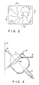
- the solution moved from the central portion to the periphery of the display screen causes an inferior, nonuniform thickness in the film at the corners of the display screen because a surface of the display screen of the cathode ray tube is convex and square. That is, in Fig. 2, when the cathode ray tube rotates in a direction indicated by arrow a , the solution applied on a portion near the central portion flows in directions indicated by arrows b . Although the solution mostly spreads outwardly, some of the solution stays at an edge portion of the display screen and flows in a direction indicated by arrows c .
- a solution which flows to the hatched portions then flows in the directions indicated by arrows d to the corners of the display screen because the display screen is convex and square. Since the speed of air flow generated at the corners is high, the solution film is dried faster in the corner areas than in the central portion, and a solution from the central portion further flows onto the dried film in the corner areas and is dried thereon, thereby forming a thick film.
- a method of forming a thin film on an outer surface of a display screen of a cathode ray tube comprising the steps of: applying a film formation material solution containing a volatile solvent on the outer surface of the display screen of the cathode ray tube to form a solution film; rotating the cathode ray tube about a tube axis thereof to obtain a uniform film thickness of the solution film; and causing a portion of the solution film applied in and around the center of the outer surface of the display screen to dry while the cathode ray tube is being rotated.
- a rotational speed of the cathode ray tube is preferably 30 to 300 rpm, and more preferably, 50 to 200 rpm. This rotational speed is preferably changed, e.g., reduced in a stepwise manner.
- An angle defined by a rotational axis of the cathode ray tube and a vertical axis is preferably 90° or less.
- the drying step can be performed by heating.
- Heating can be performed by blowing hot air or by using a heater.
- a temperature of the hot air near the display screen is preferably 30 to 200°C, and more preferably, 50 to 120°C.
- a flow speed of the hot air near the display screen is preferably 1 to 10 m/s, and more preferably, 1.5 to 6 m/s.
- the temperature and the flow speed of the air are preferably changed, e.g., increased in a stepwise manner. If drying is rapidly performed from the beginning, the solution film is dried before it attains a uniform thickness, thereby forming scale-like projections on the thin film.
- the solution film at a portion near the central portion on the outer surface of the display screen may be dried by preheating this portion up to a temperature higher than that at the corners before the solution is applied.
- a thin film having a smooth surface and a uniform film thickness can be formed on the outer surface of a display screen of a cathode ray tube.
- Fig. 3 the outer surface of display screen 12 of the 25 inch-type color cathode ray tube 11 is washed with fluoric acid, ammonium fluoride, nitric acid, or sodium hydroxide and then washed with pure water. Thereafter, a high pressure air is blown onto the outer surface of the display screen 12 to dry it. Then, tube 11 is mounted on supporting apparatus 13 so that the outer surface of screen 12 faces obliquely downward. Apparatus 13 can be inclined so that angle ⁇ defined by axis 14 of tube 11 and vertical axis 15 falls within the range of 90° or less. In this example, angle ⁇ is 15°.
- a mixed solution is applied from nozzle 16 to the entire outer surface of screen 12.
- a composition of the mixed solution is 7 g of Si(OC2H5), 176 g of isopropyl alcohol, 3 g of hydrochloric acid, and 2 g of water.
- hot air is blown from hot air supplying pipe 17 to the central portion of the outer surface of screen 12 for 10 seconds so that the temperature and flow speed of the hot air near screen 12 are about 50°C and about 2 m/sec, respectively, (a first heating step).
- the temperature of the hot air near the central portion of screen 12 is increased to about 80°C, and hot air is similarly blown for 10 seconds (a second heating step).
- the temperature of the hot air near the central portion of screen 12 is increased to 110°C, and the hot air is blown for 40 seconds (a third heating step).
- Table 1 The results of the surface check, reporting the smoothness and uniformity of the thin film surface formed as described above, are summarized in Table 1 below. Note that Table 1 also displays the results obtained when no hot air is blown, when the hot air is blown only under the heating condition of the first heating step for 60 seconds, and when air at room temperature of 22°C is blown for 100°C seconds onto the thin film surface.
- the solution film at the central portion of the outer surface of screen 12 can also be dried by preheating this portion, before the solution is applied, to a high temperature of, e.g., 40°C and preheating the corner portions with a low temperature of, e.g., 25°C.
- An angle defined by the rotational axis of the cathode ray tube and the vertical axis is preferably 90° or less. The reason for this is as follows.
- cathode ray tube 21 comprises reinforcing member 24 which serves to prevent cathode ray tube 21 from exploiding, located on side periphery 23 of display screen 22.
- a small gap is formed between side periphery 23 and reinforcing member 24.
- the solution adhered on side periphery 23 of screen 22 reaches funnel portion 28 through the gap between periphery 23 and reinforcing member 24 and is adhered on anode 26 or outer conductive film 27, thereby posing a serious problem of, e.g., poor insulation.
Landscapes
- Chemical & Material Sciences (AREA)
- Engineering & Computer Science (AREA)
- Life Sciences & Earth Sciences (AREA)
- Chemical Kinetics & Catalysis (AREA)
- General Chemical & Material Sciences (AREA)
- Geochemistry & Mineralogy (AREA)
- Materials Engineering (AREA)
- Organic Chemistry (AREA)
- Manufacturing & Machinery (AREA)
- Formation Of Various Coating Films On Cathode Ray Tubes And Lamps (AREA)
- Vessels, Lead-In Wires, Accessory Apparatuses For Cathode-Ray Tubes (AREA)
- Application Of Or Painting With Fluid Materials (AREA)
Applications Claiming Priority (4)
| Application Number | Priority Date | Filing Date | Title |
|---|---|---|---|
| JP8696687 | 1987-04-10 | ||
| JP86966/87 | 1987-04-10 | ||
| JP23812/88 | 1988-02-05 | ||
| JP2381288 | 1988-02-05 |
Publications (3)
| Publication Number | Publication Date |
|---|---|
| EP0286129A2 true EP0286129A2 (de) | 1988-10-12 |
| EP0286129A3 EP0286129A3 (en) | 1988-11-17 |
| EP0286129B1 EP0286129B1 (de) | 1990-09-26 |
Family
ID=26361233
Family Applications (1)
| Application Number | Title | Priority Date | Filing Date |
|---|---|---|---|
| EP88105646A Expired - Lifetime EP0286129B1 (de) | 1987-04-10 | 1988-04-08 | Verfahren zur Bildung eines dünnen Überzuges auf der äusseren Oberfläche eines Bildschirmes eines Elektronenstrahlröhre |
Country Status (6)
| Country | Link |
|---|---|
| US (1) | US4908232A (de) |
| EP (1) | EP0286129B1 (de) |
| JP (1) | JP2695823B2 (de) |
| KR (1) | KR930001186B1 (de) |
| CN (1) | CN1021715C (de) |
| DE (1) | DE3860680D1 (de) |
Cited By (2)
| Publication number | Priority date | Publication date | Assignee | Title |
|---|---|---|---|---|
| DE4204637C1 (de) * | 1992-02-15 | 1993-03-11 | Schott Glaswerke, 6500 Mainz, De | |
| EP0602721A1 (de) * | 1992-12-17 | 1994-06-22 | Koninklijke Philips Electronics N.V. | Verfahren zum Aushärten eines Filmes |
Families Citing this family (5)
| Publication number | Priority date | Publication date | Assignee | Title |
|---|---|---|---|---|
| KR920000328B1 (ko) * | 1988-09-29 | 1992-01-11 | 미쯔비시덴끼 가부시끼가이샤 | 대전방지 처리형 음극선관의 제조방법 |
| JPH04137436A (ja) * | 1990-09-28 | 1992-05-12 | Sony Corp | 陰極線管の製造方法 |
| CN100437152C (zh) * | 2004-09-30 | 2008-11-26 | 亚洲光学股份有限公司 | 湿式抗反射化合物薄膜的涂布方法 |
| US7993610B2 (en) * | 2005-10-05 | 2011-08-09 | Idexx Laboratories, Incorporated | Blood centrifuge rotor with fill indicator |
| CN103370286A (zh) | 2011-02-11 | 2013-10-23 | 帝斯曼知识产权资产管理有限公司 | 在基材上沉积抗反射层的方法 |
Family Cites Families (14)
| Publication number | Priority date | Publication date | Assignee | Title |
|---|---|---|---|---|
| US3143435A (en) * | 1962-01-05 | 1964-08-04 | Gen Electric | Round panel lamp phosphor coating |
| US3376153A (en) * | 1964-10-20 | 1968-04-02 | Rauland Corp | Method of coating cathode-ray tubes |
| NL6713664A (de) * | 1967-10-07 | 1969-04-09 | ||
| US3653939A (en) * | 1970-01-05 | 1972-04-04 | Zenith Radio Corp | Screening of black-surround color picture tubes |
| US4078095A (en) * | 1974-03-28 | 1978-03-07 | Rca Corporation | Slurry process for coating particles upon the viewing-window surface of a cathode-ray tube |
| US3940508A (en) * | 1974-09-16 | 1976-02-24 | Westinghouse Electric Corporation | Precoating color television picture tube faceplate panels to promote phosphor pattern adherence |
| JPS5947418B2 (ja) * | 1976-12-17 | 1984-11-19 | 株式会社東芝 | カラ−受像管の製造方法 |
| JPS54147773A (en) * | 1978-05-11 | 1979-11-19 | Mitsubishi Electric Corp | Filming method for fluorescent screen |
| JPS5512629A (en) * | 1978-07-11 | 1980-01-29 | Mitsubishi Electric Corp | Formation of organic film on the inside surface of cathode-ray tube or color picture tube |
| JPS55130039A (en) * | 1979-03-30 | 1980-10-08 | Toshiba Corp | Formation method of metal back fluorescent screen |
| JPS6074231A (ja) * | 1983-09-30 | 1985-04-26 | Hitachi Ltd | 陰極線管の製造方法 |
| JPS61104535A (ja) * | 1984-10-26 | 1986-05-22 | Hitachi Ltd | 陰極線管パネル表面の反射防止膜形成方法 |
| JPH0646538B2 (ja) * | 1985-06-19 | 1994-06-15 | 株式会社日立製作所 | ブラウン管の製造方法 |
| US4746588A (en) * | 1985-11-25 | 1988-05-24 | Rca Corporation | Method for preparing a photosensitive film on a glass surface |
-
1988
- 1988-03-23 JP JP63067120A patent/JP2695823B2/ja not_active Expired - Fee Related
- 1988-04-08 EP EP88105646A patent/EP0286129B1/de not_active Expired - Lifetime
- 1988-04-08 DE DE8888105646T patent/DE3860680D1/de not_active Expired - Lifetime
- 1988-04-08 US US07/179,326 patent/US4908232A/en not_active Expired - Lifetime
- 1988-04-09 CN CN88102016A patent/CN1021715C/zh not_active Expired - Lifetime
- 1988-04-11 KR KR1019880004102A patent/KR930001186B1/ko not_active Expired - Fee Related
Cited By (3)
| Publication number | Priority date | Publication date | Assignee | Title |
|---|---|---|---|---|
| DE4204637C1 (de) * | 1992-02-15 | 1993-03-11 | Schott Glaswerke, 6500 Mainz, De | |
| US5314715A (en) * | 1992-02-15 | 1994-05-24 | Schott Glaswerke | Coating process |
| EP0602721A1 (de) * | 1992-12-17 | 1994-06-22 | Koninklijke Philips Electronics N.V. | Verfahren zum Aushärten eines Filmes |
Also Published As
| Publication number | Publication date |
|---|---|
| KR930001186B1 (ko) | 1993-02-20 |
| CN88102016A (zh) | 1988-11-23 |
| JPH01281637A (ja) | 1989-11-13 |
| KR880013218A (ko) | 1988-11-30 |
| US4908232A (en) | 1990-03-13 |
| DE3860680D1 (de) | 1990-10-31 |
| EP0286129A3 (en) | 1988-11-17 |
| EP0286129B1 (de) | 1990-09-26 |
| CN1021715C (zh) | 1993-07-28 |
| JP2695823B2 (ja) | 1998-01-14 |
Similar Documents
| Publication | Publication Date | Title |
|---|---|---|
| US4068019A (en) | Spin coating process for prevention of edge buildup | |
| EP0286129B1 (de) | Verfahren zur Bildung eines dünnen Überzuges auf der äusseren Oberfläche eines Bildschirmes eines Elektronenstrahlröhre | |
| US3652323A (en) | Process for coating flatlike surfaces | |
| US5660876A (en) | Method of manufacturing cathode ray tube with a nonglare multi-layered film | |
| CA1087038A (en) | Process for coating a phosphor slurry on the inner surface of a color cathode ray tube faceplate | |
| US2903377A (en) | Method of applying films to cathode ray tube screens | |
| US5002799A (en) | Method for manufacturing anti-static cathode ray tubes | |
| JPH10296172A (ja) | 塗膜形成法 | |
| JP3280225B2 (ja) | ゾルゲル薄膜の成膜法 | |
| CN1146063A (zh) | 形成阴极射线管荧光屏的方法 | |
| KR100277629B1 (ko) | 필르밍액 도포방법 | |
| JPH0588001A (ja) | 陰極線管のフエース部外表面の反射防止膜形成方法 | |
| EP0574112A1 (de) | Beschichtungszusammenstellung und Kathodenstrahlröhre mit Verwendung derselben | |
| JPH03152827A (ja) | 陰極線管のフェース外表面に薄膜を形成する方法 | |
| KR920008314B1 (ko) | 음극선관의 패널 외표면에 도포막을 형성시키는 방법 | |
| JPH06283417A (ja) | 塗膜装置 | |
| US5314715A (en) | Coating process | |
| JPH08138545A (ja) | 反射・帯電防止型陰極線管の製造方法 | |
| JP3159531B2 (ja) | 受像管の製造方法 | |
| JPH0536351A (ja) | Crtアルミバツク用アンダーコート被膜の形成方法 | |
| JPH0241140B2 (ja) | Inkyokusenkannoseizohoho | |
| JP2000251754A (ja) | 蛍光面、画像表示装置及び蛍光面の製造方法 | |
| JP2002050284A (ja) | 画像表示装置用フェースパネルの表面処理方法、およびこの表面処理を施されたフェースパネルを備えた画像表示装置 | |
| JPH117889A (ja) | 陰極線管の製造方法 | |
| JPH0461726A (ja) | 小型陰極線管の成膜方法 |
Legal Events
| Date | Code | Title | Description |
|---|---|---|---|
| PUAI | Public reference made under article 153(3) epc to a published international application that has entered the european phase |
Free format text: ORIGINAL CODE: 0009012 |
|
| PUAL | Search report despatched |
Free format text: ORIGINAL CODE: 0009013 |
|
| 17P | Request for examination filed |
Effective date: 19880505 |
|
| AK | Designated contracting states |
Kind code of ref document: A2 Designated state(s): DE FR GB |
|
| AK | Designated contracting states |
Kind code of ref document: A3 Designated state(s): DE FR GB |
|
| 17Q | First examination report despatched |
Effective date: 19891227 |
|
| GRAA | (expected) grant |
Free format text: ORIGINAL CODE: 0009210 |
|
| AK | Designated contracting states |
Kind code of ref document: B1 Designated state(s): DE FR GB |
|
| REF | Corresponds to: |
Ref document number: 3860680 Country of ref document: DE Date of ref document: 19901031 |
|
| ET | Fr: translation filed | ||
| PLBE | No opposition filed within time limit |
Free format text: ORIGINAL CODE: 0009261 |
|
| STAA | Information on the status of an ep patent application or granted ep patent |
Free format text: STATUS: NO OPPOSITION FILED WITHIN TIME LIMIT |
|
| 26N | No opposition filed | ||
| REG | Reference to a national code |
Ref country code: GB Ref legal event code: 746 Effective date: 19981010 |
|
| REG | Reference to a national code |
Ref country code: FR Ref legal event code: D6 |
|
| REG | Reference to a national code |
Ref country code: GB Ref legal event code: IF02 |
|
| PGFP | Annual fee paid to national office [announced via postgrant information from national office to epo] |
Ref country code: DE Payment date: 20070405 Year of fee payment: 20 |
|
| PGFP | Annual fee paid to national office [announced via postgrant information from national office to epo] |
Ref country code: GB Payment date: 20070404 Year of fee payment: 20 |
|
| PGFP | Annual fee paid to national office [announced via postgrant information from national office to epo] |
Ref country code: FR Payment date: 20070411 Year of fee payment: 20 |
|
| REG | Reference to a national code |
Ref country code: GB Ref legal event code: PE20 Expiry date: 20080407 |
|
| PG25 | Lapsed in a contracting state [announced via postgrant information from national office to epo] |
Ref country code: GB Free format text: LAPSE BECAUSE OF EXPIRATION OF PROTECTION Effective date: 20080407 |