EP0248033B1 - Multi-level power amplifying circuitry for portable radio transceivers - Google Patents
Multi-level power amplifying circuitry for portable radio transceivers Download PDFInfo
- Publication number
- EP0248033B1 EP0248033B1 EP86906589A EP86906589A EP0248033B1 EP 0248033 B1 EP0248033 B1 EP 0248033B1 EP 86906589 A EP86906589 A EP 86906589A EP 86906589 A EP86906589 A EP 86906589A EP 0248033 B1 EP0248033 B1 EP 0248033B1
- Authority
- EP
- European Patent Office
- Prior art keywords
- power
- output
- output power
- signal
- magnitude
- Prior art date
- Legal status (The legal status is an assumption and is not a legal conclusion. Google has not performed a legal analysis and makes no representation as to the accuracy of the status listed.)
- Expired - Lifetime
Links
- 230000008878 coupling Effects 0.000 claims description 7
- 238000010168 coupling process Methods 0.000 claims description 7
- 238000005859 coupling reaction Methods 0.000 claims description 7
- 230000001105 regulatory effect Effects 0.000 claims 1
- 238000000034 method Methods 0.000 description 7
- 238000010586 diagram Methods 0.000 description 4
- 238000004891 communication Methods 0.000 description 3
- 238000013459 approach Methods 0.000 description 2
- 230000001413 cellular effect Effects 0.000 description 2
- 238000012937 correction Methods 0.000 description 1
- 230000001419 dependent effect Effects 0.000 description 1
- 238000012544 monitoring process Methods 0.000 description 1
Images


Classifications
-
- H—ELECTRICITY
- H03—ELECTRONIC CIRCUITRY
- H03F—AMPLIFIERS
- H03F3/00—Amplifiers with only discharge tubes or only semiconductor devices as amplifying elements
- H03F3/189—High-frequency amplifiers, e.g. radio frequency amplifiers
-
- H—ELECTRICITY
- H04—ELECTRIC COMMUNICATION TECHNIQUE
- H04B—TRANSMISSION
- H04B1/00—Details of transmission systems, not covered by a single one of groups H04B3/00 - H04B13/00; Details of transmission systems not characterised by the medium used for transmission
- H04B1/38—Transceivers, i.e. devices in which transmitter and receiver form a structural unit and in which at least one part is used for functions of transmitting and receiving
- H04B1/3827—Portable transceivers
- H04B1/3877—Arrangements for enabling portable transceivers to be used in a fixed position, e.g. cradles or boosters
-
- B—PERFORMING OPERATIONS; TRANSPORTING
- B32—LAYERED PRODUCTS
- B32B—LAYERED PRODUCTS, i.e. PRODUCTS BUILT-UP OF STRATA OF FLAT OR NON-FLAT, e.g. CELLULAR OR HONEYCOMB, FORM
- B32B15/00—Layered products comprising a layer of metal
-
- H—ELECTRICITY
- H03—ELECTRONIC CIRCUITRY
- H03F—AMPLIFIERS
- H03F1/00—Details of amplifiers with only discharge tubes, only semiconductor devices or only unspecified devices as amplifying elements
- H03F1/02—Modifications of amplifiers to raise the efficiency, e.g. gliding Class A stages, use of an auxiliary oscillation
- H03F1/0205—Modifications of amplifiers to raise the efficiency, e.g. gliding Class A stages, use of an auxiliary oscillation in transistor amplifiers
- H03F1/0211—Modifications of amplifiers to raise the efficiency, e.g. gliding Class A stages, use of an auxiliary oscillation in transistor amplifiers with control of the supply voltage or current
- H03F1/0216—Continuous control
- H03F1/0222—Continuous control by using a signal derived from the input signal
-
- H—ELECTRICITY
- H03—ELECTRONIC CIRCUITRY
- H03F—AMPLIFIERS
- H03F1/00—Details of amplifiers with only discharge tubes, only semiconductor devices or only unspecified devices as amplifying elements
- H03F1/02—Modifications of amplifiers to raise the efficiency, e.g. gliding Class A stages, use of an auxiliary oscillation
- H03F1/0205—Modifications of amplifiers to raise the efficiency, e.g. gliding Class A stages, use of an auxiliary oscillation in transistor amplifiers
- H03F1/0211—Modifications of amplifiers to raise the efficiency, e.g. gliding Class A stages, use of an auxiliary oscillation in transistor amplifiers with control of the supply voltage or current
- H03F1/0216—Continuous control
- H03F1/0233—Continuous control by using a signal derived from the output signal, e.g. bootstrapping the voltage supply
Definitions
- the present invention is generally related to radio transceivers and more particularly related to an improved multilevel power amplifying circuitry for use in duplex battery-operated radio transceivers.
- the maximum power output of power amplifiers in duplex battery-operated transceivers such as those used in portable radiotelephones was primarily dictated by the magnitude of the battery voltage and the need to conserve battery energy. Since vehicular operation was often desired in fringe areas, further away from the nearest fixed station than is typical in portable applications, there was a need for higher transmit power when such a portable radio transceiver is used in a vehicle. Furthermore, since the transmit and receive signals of such transceivers are duplexed, another power amplifier preceded by demultiplexing filters and followed by multiplexing filters and a separate power control circuit was required in order to boost the output power level by means of an external vehicle battery. This overall approach to boosting the output power level of such transceivers was costly and duplicative of transceiver filters, power amplifiers, and power control circuits.
- US Patent No. 4,523,155 describes power amplifier control circuitry coupled to a single power voltage, for maintaining the power amplifier output at a selected one of eight different power levels, the highest of which is limited in magnitude by the magnitude of the power supply voltage.
- EP-A-0159670 discloses a portable communication device having an amplifier which operates at a fixed output power level.
- the portable communication device can be coupled to a fixed power amplifier device which amplifies a reduced fixed output of the portable communication device by a fixed gain.
- Such a circuit requires a separate 'booster' amplifier device to provide the larger transceiver output power level.
- the present invention encompasses power amplifying circuitry for a radio frequency (RF) signal from a radio transmitter of a radio telephone, said radio telephone including a radio receiver for receiving different output power level commands each corresponding to one of a first set of output power levels, said power amplifying circuitry including amplifying means coupled to a first voltage source providing a first supply voltage for amplifying the RF signal to produce an output RF signal, selecting means for selecting one of the first set of output power levels corresponding to the received output power level command, and maintaining means for maintaining the magnitude of said output RF signal at the selected one of the first set of output power levels, said power amplifying circuitry CHARACTERIZED BY: means for coupling said amplifying means to, and operating said amplifying means from, a second voltage source providing a second supply voltage, said second supply voltage having a magnitude greater than the magnitude of said first supply voltage; means for detecting the presence of said second voltage source; said selecting means selecting one of the first set of output power levels corresponding to the received output power level
- FIG. 1 is a block diagram of a portable radio transceiver embodying the present invention together with vehicular adaptor circuitry.
- FIG 2 is a flow chart for the process used by the portable radio transceiver in Figure 1 for power level selection.
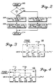
- FIGs 3, 4 and 5 are alternative embodiments of power amplifier stages for the power amplifier block in Figures 1, 8, 10 and 12.
- FIG 8 is yet another block diagram of a portable radio transceiver embodying the present invention together with vehicular adaptor circuitry.
- Figure 9 is a flow chart for the process used by the portable radio transceiver in Figure 8 to control the circuitry in the power control block thereof.
- FIG 10 is yet another block diagram of a portable radio transceiver embodying the present invention together with vehicular adaptor circuitry.
- FIG 11 is a flow chart for the process used by the portable radio transceiver in Figure 10 for power level selection.
- FIG 12 is yet another block diagram of a portable radio transceiver embodying the present invention together with vehicular adaptor circuitry.
- Figure 13 is a flow chart for the process used by the portable radio transceiver in Figure 12 for power level selection.
- Portable radio transceiver 100 embodying the present invention together with a vehicular adaptor 180.
- Portable radio transceiver 100 includes a keyboard 114, display 116, microphone 110, speaker 112, battery 118, power control 150, voltage detector 140, power amplifier (PA) 122, circulator 124, transmitter filter 126, receiver filter 130, antenna 128 and transmitter, receiver and microcomputer 120.
- Vehicular adaptor 180 includes a vehicle battery 182, battery charger 184, voltage regulator 186 and antenna 188, all of which may be commercially available devices.
- power control 150 includes a power detector 152, attenuator 154 coupled by three binary control signals to microcomputer 120, differential amplifier 156 and power control driver 158, all of which may be implemented as shown and described in U.S. Patent No. 4,523,155.
- Microcomputer 120 uses the three control signals applied to attenuator 154 to select one of eight different power levels of PA 122.
- the voltage Vref applied to differential amplifier 156 may be generated by a commercially available voltage regulator that is coupled to battery 118.
- PA 122 includes cascaded amplifier stages 132 and 134 and may also be arranged as illustrated in Figures 3, 4 and 5.
- PA 122 may be implemented with a commercially available device, such as, for example, a Motorola type MHW808 power amplifier. Likewise, circulator 124 and antenna 128 may be implemented with commercially available devices. Transmitter filter 126 and receiver filter 130 may be implemented as shown and described in U.S. Patent No. 4,431,977. Voltage detector 140 may be a conventional analog-to-digital converter (such as a Motorola type MC14442 converter) whose digitized output corresponds to the magnitude of Vsw, or may be a conventional comparator whose output changes from a low to a high state when VSW exceeds Vb by a predetermined amount.
- a Motorola type MC14442 converter such as a Motorola type MC14442 converter
- Transmitter, receiver and microcomputer 120 and associated blocks 110, 112, 114 and 116 may also be implemented by corresponding conventional circuitry shown and described in Motorola Instruction Manual no. 68P81046E60, entitled “DYNATAC Cellular Portable Telephone", or in U.S. Patent No. 4,486,624.
- This and other Motorola Instruction Manuals may be obtained from the Service Publications Department of Motorola, Inc., 1301 East Algonquin Road, Schaumburg, Illinois 60196, or from Motorola C & E Parts, 1313 East Algonquin Road, Schaumburg, Illinois 60196.
- voltage regulator 186 is optional and may be bypassed as shown by dotted line 183.
- Voltage regulator 186 both protects and optimizes the efficiency of PA 122.
- voltage regulator 186 protects PA 122 from damage due to over-voltage conditions arising during charging of vehicle battery 182 or "jump starting" of the vehicle.
- Voltage regulator 186 also optimizes the efficiency of PA 122 by maintaining Vr, and hence Vsw, at a voltage just large enough to enable PA 122 to reach the highest power level at which it is intended to operate. However, such highest power level may also be attained by bypassing voltage regulator 186 as shown by dotted line 183 without departing from the true spirit and scope of the present invention.
- Microcomputer 120 in Figure 1 senses the presence of adaptor 180 by monitoring the VEH signal from voltage detector 140. If voltage detector 140 is implemented with a commercially available comparator (e.g., a Motorola type MC1710 comparator), the VEH signal changes state when Vsw exceeds Vb by a predetermined amount. The change in state of the VEH signal informs microcomputer 120 that adaptor 180 is present. Alternalively, if voltage detector 140 is implemented with a commercially available analog-to-digital converter (e.g., a Motorola type MC14442), the VEH signal is the digital representation of the magnitude of the Vsw voltage and, for example, changes from a representation of 6V to 11V. Microcomputer 120 compares the digital values of the VEH signal to the previous value or stored predetermined values to determine that adaptor 180 is present (see also description below for block 204 in Figure 8).
- a commercially available comparator e.g., a Motorola type MC1710 comparator
- Microcomputer 120 in Figure 1 periodically monitors the VEH signal to determine when adaptor 180 is present.
- microcomputer 120 changes the operational class of transceiver 100 when adaptor 180 is present.
- the operational class is changed, for example, from class 3 to class 1 when adaptor 180 is present, and vice versa.
- power control driver 158 and PA 122 are powered by battery 118 and produces a first set of power levels for PA 122.
- the first set of power levels includes six power levels.
- a second set of power levels for PA 122 is produced.
- the second set of power levels includes eight power levels, two more power levels higher in magnitude than those in the first set.
- Additional higher power levels may be produced in operational class 1 since the voltage Vr from regulator 186 has a magnitude greater than that of the voltage from battery 118. Furthermore, the exact value of power levels 1-6 may also change from Class 1 to Class 3 in order to compensate for changes in gain between antennas 188 and 128.
- microcomputer 120 in Figure 1 is illustrated in more detail by the flow chart in Figure 2.
- the following description assumes that voltage detector 140 is a comparator.
- the flow chart is entered at START block 202 and proceeds to decision block 204 where a check is made of the VEH signal. IF the VEH signal has a first state (e.g., binary one) indicating that the adaptor 180 is present, YES branch is taken to block 206.
- the operational class of transceiver 100 is changed from class 3 to class 1.
- a power level SPL is selected from the second set of eight levels, attenuator 154 is set to produce SPL, and microcomputer 120 returns to other tasks at block 214.
- VEH signal has a second state (e.g., binary zero) indicating that the adaptor 180 is not present
- NO branch is taken to block 210.
- the operational class of transceiver 100 is changed from class 1 to class 3.
- a power level SPL is selected from the first set of six levels, attenuator 154 is set to produce SPL, and microcomputer 120 returns to other tasks at block 214.
- the various stages in PA 122 may be operated at a plurality of supply voltages for the purposes of setting its output power at a selected power level in the first or second sets of power levels and enabling PA 122 to reach higher power levels when transceiver 100 is coupled to vehicular adaptor 180.
- connecting different voltage sources to Vsw for supplying DC power to the final stage 134 of PA 122 allows the attainment of higher power levels in the second set than those in the first set of power levels.
- power control driver 158 varies the supply voltage to stage 132 in order to maintain the output of PA 122 at the level selected by microcomputer 120. Since power control driver 158 is also coupled to voltage Vsw, higher levels of DC voltage may also be applied to driver stage 132 for achieving the higher power levels in the second set of power levels.
- PA 122 is shown with two or more stages 302, 304 and 306, where DC voltage may be applied to the various stages by connection to Vsw or the power control signal.
- the connections of stages 302, 304 and 306 to Vsw and the power control signal may be configured to optimize PA performance characteristics, such as, efficiency, stability, continuity of power variation, and other requirements due to a particular application.
- FIG 4 another alternative embodiment for PA 122 is shown where the power control signal is coupled to the DC biasing point of the first stage 402.
- the DC biasing point of one or more stages may be coupled to the power control signal in order to obtain improved stability and/or power output controllability.
- This arrangement is common practice when FET devices or forward-biased bipolar devices are used as the active device in a PA stage. Since it is not necessary to raise the DC supply voltage on all PA stages in order to obtain increased power output, stages 402 and 404 may be coupled to voltage Vb from battery 118.
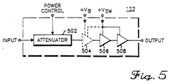
- FIG 5 yet another alternative embodiment of PA 122 is shown where the power control signal is coupled to an electronically variable attenuator 502 which varies the RF input drive power to one or more amplifier stages 504, 506 and 508.
- Attenuator 502 may be one or more PIN diodes with variable bias or a resistor network with variable resistance. Combinations of the various features found in Figures 3, 4 and 5 may also be employed as needed to provide proper functioning of the circuit chosen for PA 122.
- the key feature common to all approaches, that makes the higher power levels possible, is the raising of supply voltages to selected PA stages and/or the power control driver when adaptor 180 is connected.
- Transceiver 104 is substantially the same as transceiver 100 in Figure 1 with the exception of power control 170 and inverting gate 142.
- Power control 170 includes a power detector 172, a multiplexed analog-to-digital (A/D) converter 174, a digital-to-analog (D/A) converter 176 and power control driver 178.
- Power detector 172 and power control drive 178 may be implemented as shown and described in U.S. Patent No. 4,523,155.
- Convertors 174 and 176 may be any suitable commercially available converters, such as, for example, Motorola type MC 14442 and MC 144111 converters, respectively.
- Inverting gate 142 is coupled to adaptor 180 for generating the VEH signal.
- Microcomputer 120 in Figure 8 monitors VEH or utilizes converter 174 to determine when adaptor 180 is present.
- the VEH signal from inverting gate 142 has a binary one state when adaptor 180 is present and a binary zero state when adaptor 180 is not present. If VEH is monitored, microcomputer 120 periodically executes the flow chart in Figure 2.
- microcomputer 120 in Figure 8 may utilize converter 174 to convert
- Vsw to a digital representation which is compared to stored predetermined numbers to determine if adaptor 180 is present.
- Converter 174 periodically monitors either DPWR or Vsw in response to a select signal from microcomputer 120.
- digital representations of Vb and Vr may be stored by microcomputer 120 to determine when adaptor 180 is present.
- the flow chart in Figure 2 may be used for this purpose by changing decision block 204 to read: "Determine whether the digital representation of Vsw is greater than a digital representation of a voltage between that of Vb and Vr, such as, for example (Vb+Vr)/2". Therefore, to monitor Vsw, microcomputer 120 periodically executes the flow chart in Figure 2, and in order to maintain the selected power level, SPL, microcomputer 120 periodically executes the flow chart in Figure 9.
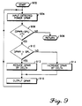
- microcomputer 120 in Figure 8 is illustrated in more detail by the flow chart in Figure 9.
- the flow chart is entered at START block 902 and proceeds to block 904 where DPWR is input from converter 174.
- DPWR is the digital representation of the output of detector 172.
- decision block 904 a check is made to see if the absolute value of DPWR-SPL is greater than TH, where SPL is a digital representation of the selected power level and TH is a predetermined number.
- TH represents a minimum difference that must exist between DPWR and SPL before a correction is made in OPWR.
- OPWR is the digital representation of the analog control signal that, when coupled to the power control driver 178, is used to make fine adjustments in the output of PA 122.
- DPWR-SPL If the absolute value of DPWR-SPL is less than TH, NO branch is taken to return to other tasks at block 908. Returning to decision block 906, if the absolute value of DPWR-SPL is greater than TH, YES branch is taken to decision block 910. In decision block 910, a check is made to see if DPWR is greater than SPL. If so, YES branch is taken to block 912 to reduce OPWR by DELTA. DELTA is a predetermined step size chosen to be small enough so that the resulting steps in DPWR are always less than TH. Otherwise, NO branch is taken from decision block 910 to block 914 where OPWR is increased by DELTA.
- OPWR is output to converter 176 and microcomputer 120 returns to block 904 to repeat the process steps of the flow chart until the absolute value of DPWR-SPL is less than TH, whereupon microcomputer 120 returns to other tasks at block 908.
- Transceiver 106 is substantially the same as transceiver 100 in Figure 1 with the exception of power control 151, inverting gate 142.
- Power control 151 contains an additional control path consisting of attenuator 155 and differential amplifier 157, which is, in turn, connected to a power control driver 189 in vehicular adaptor 181.
- Inverting gate 142 is coupled to adaptor 181 for generating the VEH signal.
- Adaptor 181 is similar to adaptor 180 with the exception of power control driver 189 which replaces voltage regulator 186.
- Power control driver 189 may be implemented in the same manner as power control driver 158 and may alternatively be located in power control 151, in which case vehicle battery 182 is coupled to plug 185.
- transceiver 106 in Figure 10 When transceiver 106 in Figure 10 is coupled by plug or otherwise to adaptor 181, battery charger 184 is coupled to battery 118, filters 120 and 130 are connected to antenna 188 instead of antenna 128, the input of inverting gate 142 is grounded, the input of power control driver 189 is connected to the output of differential amplifier 157, and Vsw is coupled to Vc2 instead of Vb.
- Vehicular adaptor 181 boosts the maximum power level of PA 122 by supplying one or more stages in PA 122 with voltage Vc2 whose magnitude may exceed the magnitude of the voltage supplied by battery 118. This is made possible by the fact that power control driver 189 is coupled to vehicle battery 182, which has a voltage of greater magnitude than that of voltage Vb from battery 118.
- Microcomputer 120 in Figure 10 periodically monitors the VEH signal from inverting gate 142 to determine when adaptor 181 is present. Switching between operational class 3 and class 1 and selection of the appropriate power level SPL from the first or second set of power levels occurs in a similar manner to that shown and described herein with respect to Figure 2.
- the selection of operational class 3 and a power level SPL from the first set of power levels is the same as that shown in Figure 2.
- maintaining a selected power level in the second set of power levels is dependent upon whether or not the magnitude of the selected power level exceeds the magnitude of the maximum power level in the first set of power levels.
- voltage Vc2 is coupled to stage 134 for attaining and maintaining such selected power level in the second set of power levels.
- microcomputer 120 in Figure 10 is illustrated in more detail by the flow chart in Figure 11.
- the flow chart is entered at START block 802 and proceeds to decision block 804 where a check is made of the VEH signal. If the VEH signal has a first state (e.g., binary zero) indicating that adaptor 181 is not present, NO branch is taken to block 806.
- the operational class of transceiver 106 is changed from class 1 to class 3.
- a power level SPL is selected from among the first set of M levels as commanded by the central control terminal.
- the power levels in the first set of M levels are preferably arranged in increasing order of magnitude such that level M has the highest magnitude.
- at block 810 attenuator 154 is set to the value needed by power control 151 to maintain the selected power level SPL, and microcomputer 120 returns to other tasks at block 822.
- a power level SPL is selected from among the second set of N power levels as commanded by the central control terminal.
- the number N of power levels in the second set is greater than the number M of power levels in the first set.
- the second set includes one or more power levels having a magnitude greater that that of level M, the highest power level in the first set.
- the magnitude of the selected power level SPL is compared to the magnitude of level M.
- Attenuator 154 is set to its maximum attenuation, which is chosen to be great enough to keep the output from attenuator 154 below the magnitude of Vref for all possible output levels from PA 122.
- power control driver 158 produces a maximum output voltage (which typically is slightly below the magnitude of voltage Vb from battery 118).
- attenuator 155 is set to the value necessary to maintain the selected power SPL using power control driver 189, and microcomputer 120 returns to other tasks at block 822.
- Attenuator 155 is set to its maximum attenuation, which is chosen to be great enough to keep the output from attenuator 155 below the magnitude of Vref for all possible output levels from PA 122.
- power control driver 189 produces a maximum output voltage Vc2 which typically has a magnitude that is slightly less than the magnitude of the voltage from vehicle battery 182.
- attenuator 154 is set to the value necessary to maintain the selected power level SPL using power control driver 158, and microcomputer 120 returns to other tasks at block 822.
- Transceiver 108 is substantially the same as transceiver 106 in Figure 10 with the exception of power control 171.
- Power control 171 contains multiplexed A/D converter 174 instead of attenuators 154 and 155, and D/A converters 176 and 177 instead of differential amplifiers 156 and 157.
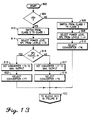
- microcomputer 120 in Figure 12 is illustrated in more detail by the flow charts in Figures 13 and 9.
- the flow chart in Figure 13 is substantially identical to the flow chart in Figure 11.
- the flow chart is entered at START block 602 and proceeds to decision block 604 where a check is made of the VEH signal. If the VEH signal has a first state (e.g., binary zero) indicating that adaptor 181 is not present, NO branch is taken to block 606.
- the operational class of transceiver 108 is changed from class 1 to class 3.
- converter 176 is selected, and microcomputer 120 exits at block 622 to block 902 in Figure 9, where the output of converter 176 is adjusted to the value needed to maintain the selected power level SPL.
- VEH signal has a second state (e.g., binary one) indicating that adaptor 181 is present
- YES branch is taken to block 612.
- the operational class is changed from class 3 to class 1.
- a power level SPL is selected from among the second set of N power levels as commanded by the central control terminal.
- the second set of N levels includes at least one level with a magnitude greater than that of level M.
- the magnitude of the selected power level SPL is compared to the magnitude of level M. If the magnitude of SPL is greater than the magnitude of level M, YES branch is taken to block 619. In block 619, converter 176 is set to its maximum output.
- power control driver 158 produces a maximum output voltage (which typically is slightly below the magnitude of voltage Vb from battery 118).
- Vb voltage
- converter 177 is selected, and microcomputer 120 exits at block 622 to block 902 in Figure 9, where the output of converter 177 is adjusted to the value needed to maintain the selected power level SPL.
- converter 177 is set to its maximum output.
- power control driver 189 produces a maximum output voltage Vc2 (which typically is slightly below the magnitude of the voltage from vehicle battery 182).
- An alternative implementation of block 617 is to set converter 177 such that power control driver 189 produces an output voltage substantially equal in magnitude to that produced by battery 118.
- converter 176 is selected, and microcomputer 120 exits at block 622 to block 902 in Figure 9, where the output of converter 176 is adjusted to the value needed to maintain the selected power level SPL.
- multi-level power amplifying circuitry may be advantageously utilized in portable radio transceivers which are insertable into a vehicular adaptor for operation from the vehicle battery.
- the power amplifier Upon detecting the presence of the vehicular adaptor, the power amplifier be operated at a second set of power levels which include levels greater than those in a first set of power levels for portable operation.
- the multi-level power amplifying circuitry of the present invention may be advantageously utilized in a variety of applications where battery-operated radio transceivers may be inserted into an adaptor for operation from another power source.
Landscapes
- Engineering & Computer Science (AREA)
- Power Engineering (AREA)
- Computer Networks & Wireless Communication (AREA)
- Signal Processing (AREA)
- Transmitters (AREA)
- Amplifiers (AREA)
- Transceivers (AREA)
Applications Claiming Priority (2)
| Application Number | Priority Date | Filing Date | Title |
|---|---|---|---|
| US06/794,026 US4636741A (en) | 1985-11-01 | 1985-11-01 | Multi-level power amplifying circuitry for portable radio transceivers |
| US794026 | 1985-11-01 |
Publications (3)
| Publication Number | Publication Date |
|---|---|
| EP0248033A4 EP0248033A4 (en) | 1987-11-02 |
| EP0248033A1 EP0248033A1 (en) | 1987-12-09 |
| EP0248033B1 true EP0248033B1 (en) | 1992-02-05 |
Family
ID=25161452
Family Applications (1)
| Application Number | Title | Priority Date | Filing Date |
|---|---|---|---|
| EP86906589A Expired - Lifetime EP0248033B1 (en) | 1985-11-01 | 1986-10-08 | Multi-level power amplifying circuitry for portable radio transceivers |
Country Status (10)
| Country | Link |
|---|---|
| US (1) | US4636741A (ja) |
| EP (1) | EP0248033B1 (ja) |
| JP (1) | JP2579473B2 (ja) |
| KR (1) | KR960002390B1 (ja) |
| CN (1) | CN1006269B (ja) |
| AU (1) | AU582078B2 (ja) |
| CA (1) | CA1264067A (ja) |
| DE (1) | DE3683848D1 (ja) |
| IL (1) | IL80141A (ja) |
| WO (1) | WO1987002843A1 (ja) |
Families Citing this family (112)
| Publication number | Priority date | Publication date | Assignee | Title |
|---|---|---|---|---|
| JPH0644716B2 (ja) * | 1984-08-14 | 1994-06-08 | 日本電気株式会社 | 無線通信装置 |
| US4885798A (en) * | 1987-01-28 | 1989-12-05 | Rockwell International Corporation | Power consumption control apparatus |
| JPS648733A (en) * | 1987-06-30 | 1989-01-12 | Mitsubishi Electric Corp | Portable radio communication equipment |
| JPS6446324A (en) * | 1987-08-14 | 1989-02-20 | Fujitsu Ltd | Control circuit for switching transmission power of portable radio equipment |
| JPS6485431A (en) * | 1987-09-28 | 1989-03-30 | Toshiba Corp | Radio telephone system |
| US5029233A (en) * | 1987-10-09 | 1991-07-02 | Motorola, Inc. | Radio arrangement having two radios sharing circuitry |
| US4875038A (en) * | 1988-01-07 | 1989-10-17 | Motorola, Inc. | Frequency division multiplexed acknowledge back paging system |
| US4825193A (en) * | 1988-01-07 | 1989-04-25 | Motorola, Inc. | Acknowledge back pager with adaptive variable transmitter output power |
| US4891637A (en) * | 1988-01-07 | 1990-01-02 | Motorola, Inc. | Acknowledge back pager with apparatus for controlling transmit frequency |
| US4882579A (en) * | 1988-01-07 | 1989-11-21 | Motorola, Inc. | Code division multiplexed acknowledge back paging system |
| US4823123A (en) * | 1988-01-07 | 1989-04-18 | Motorola, Inc. | Knowledge back pager with frequency control apparatus |
| JPH0650825B2 (ja) * | 1988-01-29 | 1994-06-29 | 日本電気株式会社 | 無線電話装置 |
| JPH01220919A (ja) * | 1988-02-29 | 1989-09-04 | Toshiba Corp | 無線電話装置 |
| JPH0759109B2 (ja) * | 1988-04-20 | 1995-06-21 | 日本電気株式会社 | 終話処理機能付自動車電話端末機 |
| US5203020A (en) * | 1988-06-14 | 1993-04-13 | Kabushiki Kaisha Toshiba | Method and apparatus for reducing power consumption in a radio telecommunication apparatus |
| JP2583578B2 (ja) * | 1988-07-01 | 1997-02-19 | 三菱電機株式会社 | ポケット電話機 |
| US5150031A (en) * | 1988-09-30 | 1992-09-22 | Motorola, Inc. | Battery charging system |
| US5095528A (en) * | 1988-10-28 | 1992-03-10 | Orion Industries, Inc. | Repeater with feedback oscillation control |
| US5170494A (en) * | 1988-12-08 | 1992-12-08 | Nokia Mobile Phones Ltd. | Two piece radio telephone |
| GB8828635D0 (en) * | 1988-12-08 | 1989-01-11 | Hewlett Packard Co | Rf amplifier bias circuit |
| US4989261A (en) * | 1988-12-09 | 1991-01-29 | Dallas Semiconductor Corporation | Power supply intercept with reference output |
| JPH02202252A (ja) * | 1989-01-31 | 1990-08-10 | Toshiba Corp | コードレス電話装置の充電器 |
| JP2773228B2 (ja) * | 1989-04-20 | 1998-07-09 | 日本電気株式会社 | 携帯電話機 |
| US5164652A (en) * | 1989-04-21 | 1992-11-17 | Motorola, Inc. | Method and apparatus for determining battery type and modifying operating characteristics |
| KR910007680B1 (ko) * | 1989-04-26 | 1991-09-30 | 삼성전자 주식회사 | 휴대용 이동 무선전화기의 rf 전력 레벨 제어회로 |
| US4989260A (en) * | 1989-05-17 | 1991-01-29 | The Quaker Oats Company | Transmitter with power reduction to compensate for varying radiated electric field strength when switching between batteries and AC power |
| US5142279A (en) * | 1989-06-05 | 1992-08-25 | Motorola, Inc. | Acknowledge back paging system having the capability of matching variable length data messages to pager addresses |
| JPH0775324B2 (ja) * | 1989-08-18 | 1995-08-09 | 日本電気株式会社 | 携帯無線機 |
| ES2073541T3 (es) * | 1989-12-05 | 1995-08-16 | Nec Corp | Unidad amplificadora de potencia que utiliza un modulo amplificador de potencia. |
| JP2616098B2 (ja) * | 1990-02-27 | 1997-06-04 | 日本電気株式会社 | 電力増幅装置 |
| JP2647730B2 (ja) * | 1990-06-01 | 1997-08-27 | ソニー株式会社 | 移動電話装置 |
| TW198152B (ja) * | 1990-10-18 | 1993-01-11 | Hitachi Seisakusyo Kk | |
| GB9025007D0 (en) * | 1990-11-16 | 1991-01-02 | Orbitel Mobile Communications | Mobile radio telephone |
| BR9106405A (pt) * | 1990-12-20 | 1993-05-04 | Motorola Inc | Circuidade de controle de energia,telefone celular de acesso multiplo de divisao de tempo |
| JPH04239251A (ja) * | 1991-01-11 | 1992-08-27 | Toshiba Corp | 無線電話装置アダプタ |
| JP3058923B2 (ja) * | 1991-01-11 | 2000-07-04 | 株式会社東芝 | 無線電話装置アダプタ |
| US5444867A (en) * | 1991-01-11 | 1995-08-22 | Kabushiki Kaisha Toshiba | Adapter unit for adaptively supplying a portable radio telephone with power |
| JPH04319899A (ja) * | 1991-04-19 | 1992-11-10 | Fujitsu Ltd | 自動車電話付属回路 |
| US5287555A (en) * | 1991-07-22 | 1994-02-15 | Motorola, Inc. | Power control circuitry for a TDMA radio frequency transmitter |
| GB2258370B (en) * | 1991-08-02 | 1995-09-06 | Technophone Ltd | Cellular telephone |
| US5265271A (en) * | 1991-09-23 | 1993-11-23 | Motorola, Inc. | Low battery detector |
| US5303395A (en) * | 1991-11-06 | 1994-04-12 | Mitsubishi Consumer Electronics America, Inc. | Power control with a constant gain amplifier for portable radio transceivers |
| JP2776105B2 (ja) * | 1992-01-07 | 1998-07-16 | 三菱電機株式会社 | 電子機器及び電子機器への電力供給方法 |
| EP0559187B1 (en) * | 1992-03-06 | 1998-11-04 | Fujitsu Limited | Adapter for connecting a portable telephone to a mobile telephone |
| US5333176A (en) * | 1992-04-30 | 1994-07-26 | Murata Machinery, Ltd. | Cellular hand held portable speakerphone system having an interface adapter |
| JP2935311B2 (ja) * | 1992-07-24 | 1999-08-16 | 関西日本電気株式会社 | 充電回路 |
| JPH06260996A (ja) * | 1992-10-02 | 1994-09-16 | Nokia Mobile Phones Ltd | セルラ電話用出力増幅システム |
| US5457814A (en) * | 1993-10-02 | 1995-10-10 | Nokia Mobile Phones Ltd. | Power boost system for cellular telephone |
| US5436548A (en) * | 1992-11-25 | 1995-07-25 | Motorola, Inc. | Battery charging and discharging system and corresponding method |
| KR950007973B1 (ko) * | 1992-11-27 | 1995-07-21 | 삼성전자주식회사 | 휴대용 무선송수신기의 고주파 출력레벨 보상회로 |
| US5332928A (en) * | 1992-12-10 | 1994-07-26 | Threepenny Electronics Corporation | Battery drain reducer |
| AU5986594A (en) * | 1992-12-30 | 1994-08-15 | George H. Grindley Jr. | Programmable child paging system |
| JPH06276146A (ja) * | 1993-03-19 | 1994-09-30 | Fujitsu Ltd | 移動電話装置 |
| FI99180C (fi) * | 1993-04-26 | 1997-10-10 | Nokia Mobile Phones Ltd | Menetelmä radiopuhelimen käyttämiseksi ulkoisen vahvistinlaitteen kanssa ja menetelmässä käytettävä radiopuhelin ja vahvistinlaite |
| US5432473A (en) * | 1993-07-14 | 1995-07-11 | Nokia Mobile Phones, Limited | Dual mode amplifier with bias control |
| JP2570588B2 (ja) * | 1993-07-29 | 1997-01-08 | 日本電気株式会社 | 送受信装置 |
| JP3158833B2 (ja) * | 1994-01-27 | 2001-04-23 | 三菱電機株式会社 | 移動無線装置 |
| US5629599A (en) * | 1994-05-31 | 1997-05-13 | Motorola, Inc. | Rechargeable battery-powered communication device having integral vibrating means |
| US5697074A (en) * | 1995-03-30 | 1997-12-09 | Nokia Mobile Phones Limited | Dual rate power control loop for a transmitter |
| US5732335A (en) * | 1995-04-28 | 1998-03-24 | Telefonaktiebolaget Lm Ericsson | Externally controlled output power by means of antenna keying |
| US5689815A (en) * | 1995-05-04 | 1997-11-18 | Oki Telecom, Inc. | Saturation prevention system for radio telephone with open and closed loop power control systems |
| US5754962A (en) * | 1995-07-27 | 1998-05-19 | Ericsson Inc. | Method and apparatus for indicating an operable or non-operable connection between a portable radio and a vehicle kit |
| JP3039613B2 (ja) * | 1995-08-28 | 2000-05-08 | 日本電気株式会社 | 増幅器 |
| US5623227A (en) * | 1995-10-17 | 1997-04-22 | Motorola, Inc. | Amplifier circuit and method of controlling an amplifier for use in a radio frequency communication system |
| US5621354A (en) * | 1995-10-17 | 1997-04-15 | Motorola, Inc. | Apparatus and method for performing error corrected amplification in a radio frequency system |
| JP3309271B2 (ja) * | 1996-07-09 | 2002-07-29 | 京セラ株式会社 | 携帯端末 |
| US5752172A (en) * | 1996-08-16 | 1998-05-12 | Nokia Mobile Phones Limited | Distributed transmitter output power control circuit and method for a radio telephone |
| US5898908A (en) * | 1996-10-09 | 1999-04-27 | Ericsson, Inc. | RF gain enhancement for cellular telephone |
| US5802167A (en) * | 1996-11-12 | 1998-09-01 | Hong; Chu-Chai | Hands-free device for use with a cellular telephone in a car to permit hands-free operation of the cellular telephone |
| FR2758024B1 (fr) * | 1996-12-30 | 1999-01-29 | Alsthom Cge Alcatel | Dispositif d'alimentation d'un amplificateur de puissance pour terminal de radiocommunications mobiles |
| DE19705447B4 (de) * | 1997-02-13 | 2006-02-02 | Robert Bosch Gmbh | Funkgerät |
| US6230031B1 (en) | 1997-03-31 | 2001-05-08 | Oki Telecom, Inc. | Power amplifying circuitry for wireless radio transceivers |
| US6236863B1 (en) | 1997-03-31 | 2001-05-22 | Oki Telecom, Inc. | Comprehensive transmitter power control system for radio telephones |
| US6148220A (en) * | 1997-04-25 | 2000-11-14 | Triquint Semiconductor, Inc. | Battery life extending technique for mobile wireless applications |
| US6029074A (en) * | 1997-05-02 | 2000-02-22 | Ericsson, Inc. | Hand-held cellular telephone with power management features |
| US6185431B1 (en) | 1997-06-18 | 2001-02-06 | Oki Telecom, Inc. | Mobile station closed loop output power stability system for weak signal conditions |
| US5999832A (en) * | 1997-07-31 | 1999-12-07 | Vannatta; Louis J. | Method of and apparatus for controlling a transmit power of a communication device |
| US6011323A (en) * | 1997-09-30 | 2000-01-04 | International Business Machines Corporation | Apparatus, method and article of manufacture providing for auxiliary battery conservation in adapters |
| US6038457A (en) * | 1997-12-05 | 2000-03-14 | Motorola, Inc. | Apparatus and method for detecting and powering an accessory |
| US6097973A (en) * | 1997-12-19 | 2000-08-01 | Motorola, Inc. | Electronic circuit for a portable electronic device |
| EP0940910A1 (en) * | 1998-03-03 | 1999-09-08 | Robert Bosch Gmbh | Power amplifier for a radio transmitter and mobile telephone with a radio transmitter |
| GB2339113B (en) * | 1998-06-30 | 2003-05-21 | Nokia Mobile Phones Ltd | Data transmission in tdma system |
| US6133792A (en) * | 1998-09-17 | 2000-10-17 | Telefonakteibolaget Lm Ericsson | Method and apparatus for preventing power amplifier saturation |
| DE19858836A1 (de) * | 1998-12-19 | 2000-06-21 | Bayerische Motoren Werke Ag | Fahrzeug-Audiosystem |
| JP2000332542A (ja) * | 1999-05-20 | 2000-11-30 | Mitsubishi Electric Corp | 多段電力増幅器のバイアス回路及びそのバイアス供給方法 |
| US6734724B1 (en) | 2000-10-06 | 2004-05-11 | Tropian, Inc. | Power control and modulation of switched-mode power amplifiers with one or more stages |
| US6941152B2 (en) * | 2001-04-24 | 2005-09-06 | Ipr Licensing, Inc. | Wireless subscriber network registration system for configurable services |
| FR2824972B1 (fr) * | 2001-05-17 | 2003-12-26 | Sagem | Selection de puissance d'emission dans un radiotelephone |
| US6515541B2 (en) * | 2001-06-13 | 2003-02-04 | Skyworks Solutions, Inc. | Multi-level power amplifier |
| US7039435B2 (en) * | 2001-09-28 | 2006-05-02 | Agere Systems Inc. | Proximity regulation system for use with a portable cell phone and a method of operation thereof |
| TW516748U (en) * | 2001-10-26 | 2003-01-01 | Kye Systems Corp | Wireless transmitting circuit with adjustable radio frequency transmitting power |
| US6892080B2 (en) * | 2001-11-27 | 2005-05-10 | Arrista Technologies, Inc. | Booster amplifier for cellular telephone cradles |
| US6624702B1 (en) | 2002-04-05 | 2003-09-23 | Rf Micro Devices, Inc. | Automatic Vcc control for optimum power amplifier efficiency |
| DE10218828A1 (de) * | 2002-04-26 | 2003-11-06 | Siemens Ag | Mobilfunkgerät mit Sendeleistungsbeschränkung |
| US6685334B2 (en) | 2002-04-30 | 2004-02-03 | G-5 Electronics | System and method of power management for a solar powered device |
| US20040072554A1 (en) * | 2002-10-15 | 2004-04-15 | Triquint Semiconductor, Inc. | Automatic-bias amplifier circuit |
| US7010284B2 (en) * | 2002-11-06 | 2006-03-07 | Triquint Semiconductor, Inc. | Wireless communications device including power detector circuit coupled to sample signal at interior node of amplifier |
| US20040070454A1 (en) * | 2002-10-15 | 2004-04-15 | Triquint Semiconductor, Inc. | Continuous bias circuit and method for an amplifier |
| US7136667B2 (en) * | 2003-10-28 | 2006-11-14 | Nokia Corporation | Method and radio terminal equipment arrangement for power control, radio terminal equipment and secondary terminal unit |
| US7177370B2 (en) * | 2003-12-17 | 2007-02-13 | Triquint Semiconductor, Inc. | Method and architecture for dual-mode linear and saturated power amplifier operation |
| GB2411547A (en) * | 2004-02-27 | 2005-08-31 | Nec Technologies | Dynamically determining a power class of a mobile radio communications device |
| US7498953B2 (en) * | 2004-11-16 | 2009-03-03 | Salser Jr Floyd Stanley | Smart transmitter for utility meters |
| EP1708358A3 (en) * | 2005-03-11 | 2006-12-06 | LG Electronics Inc. | Mobile communications terminal having driving voltage control apparatus and method thereof |
| DE102006056342B4 (de) * | 2005-11-30 | 2011-07-14 | VTECH Telecommunications, Ltd., New Territory | System und Verfahren zur Registrierung eines drahtlosen Handgeräts |
| US20080003956A1 (en) * | 2006-06-29 | 2008-01-03 | Paul Stanley Rutkowski | Apparatus and method for FM transmitting audio at optimal power levels |
| KR100765790B1 (ko) | 2006-06-30 | 2007-10-12 | 삼성전자주식회사 | 모바일 기기의 가변 전원공급 장치 및 방법 |
| US8798564B2 (en) * | 2009-03-17 | 2014-08-05 | Provigent Ltd. | Transmitter with replaceable power amplifier |
| US8611836B2 (en) * | 2010-08-25 | 2013-12-17 | Skyworks Solutions, Inc. | Amplifier gain adjustment in response to reduced supply voltage |
| US11483778B2 (en) * | 2019-07-16 | 2022-10-25 | Molex CVS Bochum GmbH | Compensator system with feedback |
| US11272459B2 (en) * | 2019-11-07 | 2022-03-08 | Qualcomm Incorporated | Power control for wireless device cooperative transmission schemes |
| CN114946084A (zh) | 2020-01-24 | 2022-08-26 | 京瓷Avx元器件(圣地亚哥)有限公司 | 用于具有模态天线的天线系统的射频rf放大器电路 |
| US11533688B2 (en) * | 2021-03-17 | 2022-12-20 | T-Mobile Usa, Inc. | Dynamic switching of user equipment power class |
Family Cites Families (9)
| Publication number | Priority date | Publication date | Assignee | Title |
|---|---|---|---|---|
| US3065424A (en) * | 1960-12-20 | 1962-11-20 | Packard Bell Electronics Corp | Radio receiver with means for compensating for variations in the supply voltage |
| US4307455A (en) * | 1978-02-27 | 1981-12-22 | Rockwell International Corporation | Power supply for computing means with data protected shut-down |
| DE2911998C2 (de) * | 1979-03-27 | 1985-11-07 | Robert Bosch Gmbh, 7000 Stuttgart | Stromversorgung für einen Mikroprozessor, der elektrische Einrichtungen, insbesondere eines Kraftfahrzeuges steuert |
| US4414623A (en) * | 1980-10-01 | 1983-11-08 | Motorola, Inc. | Dual deadman timer circuit |
| JPS5851634A (ja) * | 1981-09-24 | 1983-03-26 | Nippon Telegr & Teleph Corp <Ntt> | 移動通信方式 |
| JPS5981113U (ja) * | 1982-11-25 | 1984-06-01 | 日本電気株式会社 | 出力電力制御回路 |
| US4523155A (en) * | 1983-05-04 | 1985-06-11 | Motorola, Inc. | Temperature compensated automatic output control circuitry for RF signal power amplifiers with wide dynamic range |
| WO1985000082A1 (en) * | 1983-06-17 | 1985-01-03 | Prutec Limited | Transmitter with power amplifier control |
| JPS60223231A (ja) * | 1984-04-19 | 1985-11-07 | Nec Corp | 無線通信機 |
-
1985
- 1985-11-01 US US06/794,026 patent/US4636741A/en not_active Expired - Lifetime
-
1986
- 1986-09-24 IL IL80141A patent/IL80141A/xx not_active IP Right Cessation
- 1986-09-25 CA CA000519045A patent/CA1264067A/en not_active Expired
- 1986-10-08 DE DE8686906589T patent/DE3683848D1/de not_active Expired - Lifetime
- 1986-10-08 KR KR1019870700572A patent/KR960002390B1/ko not_active IP Right Cessation
- 1986-10-08 AU AU65439/86A patent/AU582078B2/en not_active Ceased
- 1986-10-08 EP EP86906589A patent/EP0248033B1/en not_active Expired - Lifetime
- 1986-10-08 JP JP61505717A patent/JP2579473B2/ja not_active Expired - Lifetime
- 1986-10-08 WO PCT/US1986/002140 patent/WO1987002843A1/en active IP Right Grant
- 1986-10-30 CN CN86107133.6A patent/CN1006269B/zh not_active Expired
Also Published As
| Publication number | Publication date |
|---|---|
| AU582078B2 (en) | 1989-03-09 |
| JPS63501258A (ja) | 1988-05-12 |
| KR960002390B1 (ko) | 1996-02-16 |
| WO1987002843A1 (en) | 1987-05-07 |
| IL80141A (en) | 1990-07-12 |
| US4636741A (en) | 1987-01-13 |
| EP0248033A1 (en) | 1987-12-09 |
| IL80141A0 (en) | 1986-12-31 |
| CN86107133A (zh) | 1987-06-10 |
| DE3683848D1 (de) | 1992-03-19 |
| EP0248033A4 (en) | 1987-11-02 |
| JP2579473B2 (ja) | 1997-02-05 |
| KR880700537A (ko) | 1988-03-15 |
| AU6543986A (en) | 1987-05-19 |
| CA1264067A (en) | 1989-12-27 |
| CN1006269B (zh) | 1989-12-27 |
Similar Documents
| Publication | Publication Date | Title |
|---|---|---|
| EP0248033B1 (en) | Multi-level power amplifying circuitry for portable radio transceivers | |
| US5303395A (en) | Power control with a constant gain amplifier for portable radio transceivers | |
| CA1245307A (en) | Battery-powered radio communication apparatus capable of prolonging the communicable state thereof | |
| CA1233204A (en) | Automatic output control circuitry for rf power amplifiers with wide dynamic range | |
| US5852770A (en) | Transmission power control device for a portable terminal | |
| EP0734118B1 (en) | Bias control circuit for an RF power amplifier | |
| CA2160750C (en) | Method and apparatus for increasing amplifier efficiency | |
| CA1230926A (en) | Radio communication device and method of controlling transmitter output power | |
| EP0482502B1 (en) | Power amplifier and mobile radio apparatus with the same | |
| US5438683A (en) | Automatic level control circuit for dual mode analog/digital cellular telephone | |
| US5029298A (en) | Transmitter circuit | |
| JPH0376430A (ja) | 携帯無線機 | |
| WO1993018583A1 (en) | High efficiency dual mode power amplifier apparatus | |
| EP0459440B1 (en) | Radio transmitter apparatus | |
| US20010006355A1 (en) | Device for controlling power in power amplifier of a portable wireless terminal | |
| US5239695A (en) | Radio-frequency power control circuit of mobile radiophone | |
| KR910007680B1 (ko) | 휴대용 이동 무선전화기의 rf 전력 레벨 제어회로 | |
| US6175748B1 (en) | Methods and apparatus for determination of a power level in an RF booster for wireless communications | |
| JP3180429B2 (ja) | 移動電話装置 | |
| JPS6047783B2 (ja) | 自動利得制御方式 | |
| WO1985000082A1 (en) | Transmitter with power amplifier control | |
| GB2308950A (en) | Power supply for intermittent load | |
| JPH05268139A (ja) | 電力増幅回路 | |
| JPH05160771A (ja) | 携帯電話装置 | |
| US20040072548A1 (en) | Transmission circuit suitable for dual-mode mobile phone |
Legal Events
| Date | Code | Title | Description |
|---|---|---|---|
| PUAI | Public reference made under article 153(3) epc to a published international application that has entered the european phase |
Free format text: ORIGINAL CODE: 0009012 |
|
| 17P | Request for examination filed |
Effective date: 19870630 |
|
| AK | Designated contracting states |
Kind code of ref document: A1 Designated state(s): DE FR IT NL SE |
|
| A4 | Supplementary search report drawn up and despatched |
Effective date: 19871102 |
|
| 17Q | First examination report despatched |
Effective date: 19891218 |
|
| GRAA | (expected) grant |
Free format text: ORIGINAL CODE: 0009210 |
|
| ITF | It: translation for a ep patent filed |
Owner name: BARZANO' E ZANARDO ROMA S.P.A. |
|
| AK | Designated contracting states |
Kind code of ref document: B1 Designated state(s): DE FR IT NL SE |
|
| REF | Corresponds to: |
Ref document number: 3683848 Country of ref document: DE Date of ref document: 19920319 |
|
| ET | Fr: translation filed | ||
| PLBI | Opposition filed |
Free format text: ORIGINAL CODE: 0009260 |
|
| PLAB | Opposition data, opponent's data or that of the opponent's representative modified |
Free format text: ORIGINAL CODE: 0009299OPPO |
|
| 26 | Opposition filed |
Opponent name: NOKIA MOBILE PHONES LTD Effective date: 19921104 |
|
| R26 | Opposition filed (corrected) |
Opponent name: NOKIA MOBILE PHONES LTD Effective date: 19921104 |
|
| NLR1 | Nl: opposition has been filed with the epo |
Opponent name: NOKIA MOBILE PHONES LTD |
|
| EAL | Se: european patent in force in sweden |
Ref document number: 86906589.6 |
|
| PGFP | Annual fee paid to national office [announced via postgrant information from national office to epo] |
Ref country code: NL Payment date: 19961031 Year of fee payment: 11 |
|
| APCC | Communication from the board of appeal sent |
Free format text: ORIGINAL CODE: EPIDOS OBAPO |
|
| APCC | Communication from the board of appeal sent |
Free format text: ORIGINAL CODE: EPIDOS OBAPO |
|
| APAC | Appeal dossier modified |
Free format text: ORIGINAL CODE: EPIDOS NOAPO |
|
| PLBN | Opposition rejected |
Free format text: ORIGINAL CODE: 0009273 |
|
| STAA | Information on the status of an ep patent application or granted ep patent |
Free format text: STATUS: OPPOSITION REJECTED |
|
| 27O | Opposition rejected |
Effective date: 19971015 |
|
| PG25 | Lapsed in a contracting state [announced via postgrant information from national office to epo] |
Ref country code: NL Free format text: LAPSE BECAUSE OF NON-PAYMENT OF DUE FEES Effective date: 19980501 |
|
| NLR2 | Nl: decision of opposition | ||
| NLV4 | Nl: lapsed or anulled due to non-payment of the annual fee |
Effective date: 19980501 |
|
| PGFP | Annual fee paid to national office [announced via postgrant information from national office to epo] |
Ref country code: SE Payment date: 19991014 Year of fee payment: 14 |
|
| PGFP | Annual fee paid to national office [announced via postgrant information from national office to epo] |
Ref country code: DE Payment date: 19991021 Year of fee payment: 14 |
|
| PG25 | Lapsed in a contracting state [announced via postgrant information from national office to epo] |
Ref country code: SE Free format text: THE PATENT HAS BEEN ANNULLED BY A DECISION OF A NATIONAL AUTHORITY Effective date: 20001030 |
|
| EUG | Se: european patent has lapsed |
Ref document number: 86906589.6 |
|
| PG25 | Lapsed in a contracting state [announced via postgrant information from national office to epo] |
Ref country code: DE Free format text: LAPSE BECAUSE OF NON-PAYMENT OF DUE FEES Effective date: 20010703 |
|
| APAH | Appeal reference modified |
Free format text: ORIGINAL CODE: EPIDOSCREFNO |
|
| PGFP | Annual fee paid to national office [announced via postgrant information from national office to epo] |
Ref country code: FR Payment date: 20051006 Year of fee payment: 20 |
|
| PG25 | Lapsed in a contracting state [announced via postgrant information from national office to epo] |
Ref country code: IT Free format text: LAPSE BECAUSE OF NON-PAYMENT OF DUE FEES;WARNING: LAPSES OF ITALIAN PATENTS WITH EFFECTIVE DATE BEFORE 2007 MAY HAVE OCCURRED AT ANY TIME BEFORE 2007. THE CORRECT EFFECTIVE DATE MAY BE DIFFERENT FROM THE ONE RECORDED. Effective date: 20051008 |
|
| P01 | Opt-out of the competence of the unified patent court (upc) registered |
Effective date: 20230520 |