EP0243840B1 - Steuerschaltung für einen Umrichter - Google Patents
Steuerschaltung für einen Umrichter Download PDFInfo
- Publication number
- EP0243840B1 EP0243840B1 EP87105791A EP87105791A EP0243840B1 EP 0243840 B1 EP0243840 B1 EP 0243840B1 EP 87105791 A EP87105791 A EP 87105791A EP 87105791 A EP87105791 A EP 87105791A EP 0243840 B1 EP0243840 B1 EP 0243840B1
- Authority
- EP
- European Patent Office
- Prior art keywords
- current
- voltage
- control
- inverter
- control circuit
- Prior art date
- Legal status (The legal status is an assumption and is not a legal conclusion. Google has not performed a legal analysis and makes no representation as to the accuracy of the status listed.)
- Expired - Lifetime
Links
Images


Classifications
-
- H—ELECTRICITY
- H02—GENERATION; CONVERSION OR DISTRIBUTION OF ELECTRIC POWER
- H02M—APPARATUS FOR CONVERSION BETWEEN AC AND AC, BETWEEN AC AND DC, OR BETWEEN DC AND DC, AND FOR USE WITH MAINS OR SIMILAR POWER SUPPLY SYSTEMS; CONVERSION OF DC OR AC INPUT POWER INTO SURGE OUTPUT POWER; CONTROL OR REGULATION THEREOF
- H02M7/00—Conversion of AC power input into DC power output; Conversion of DC power input into AC power output
- H02M7/42—Conversion of DC power input into AC power output without possibility of reversal
- H02M7/44—Conversion of DC power input into AC power output without possibility of reversal by static converters
- H02M7/48—Conversion of DC power input into AC power output without possibility of reversal by static converters using discharge tubes with control electrode or semiconductor devices with control electrode
- H02M7/53—Conversion of DC power input into AC power output without possibility of reversal by static converters using discharge tubes with control electrode or semiconductor devices with control electrode using devices of a triode or transistor type requiring continuous application of a control signal
- H02M7/537—Conversion of DC power input into AC power output without possibility of reversal by static converters using discharge tubes with control electrode or semiconductor devices with control electrode using devices of a triode or transistor type requiring continuous application of a control signal using semiconductor devices only, e.g. single switched pulse inverters
- H02M7/5387—Conversion of DC power input into AC power output without possibility of reversal by static converters using discharge tubes with control electrode or semiconductor devices with control electrode using devices of a triode or transistor type requiring continuous application of a control signal using semiconductor devices only, e.g. single switched pulse inverters in a bridge configuration
- H02M7/53871—Conversion of DC power input into AC power output without possibility of reversal by static converters using discharge tubes with control electrode or semiconductor devices with control electrode using devices of a triode or transistor type requiring continuous application of a control signal using semiconductor devices only, e.g. single switched pulse inverters in a bridge configuration with automatic control of output voltage or current
- H02M7/53873—Conversion of DC power input into AC power output without possibility of reversal by static converters using discharge tubes with control electrode or semiconductor devices with control electrode using devices of a triode or transistor type requiring continuous application of a control signal using semiconductor devices only, e.g. single switched pulse inverters in a bridge configuration with automatic control of output voltage or current with digital control
Definitions
- the invention relates to a control circuit in a power conversion apparatus producing sinusoidal a.c. power through multiple switching operations of switching devices within a cycle and supplying through an L-C type output filter having a series reactor and a parallel capacitor sinusoidal voltage to a load, using voltage feedback and current feedback.
- FIG. 1 is a block diagram derived from FIG. 5 of the above article on page 207 and rewritten to contrast with the present invention.
- the system includes an inverter main circuit 1, a reactor 2 and capacitor 3 making in combination an alternating current (AC) power filter, a direct current (DC) power source 4, a load 5, a drive circuit 6 for the inverter main circuit 1, an AC reference voltage generator 7 for producing a sinusoidal reference voltage, an amplifier 8, and a pulse width modulation (PWM) circuit 9 consisting of a comparator 9a and a carrier wave generator 9b.
- AC alternating current
- DC direct current
- PWM pulse width modulation
- a sinusoidal output voltage in compliance with the control output of the PWM circuit 9 is produced across the capacitor 3.
- the amplifier 8 and PWM circuit 9 control the switching operation of the inverter 1 so that the output voltage is equal to the sinusoidal reference voltage of the AC reference voltage generator 7.
- the PWM circuit 9 made up of a triangular carrier wave generator 9b and a comparator 9a, operates to determine the switching time point of pulse width modulation in accordance with a virtually sinusoidal signal produced by amplification of the voltage difference by the amplifier 8. Since the amplifier 8 has a certain finite gain for the stability of operation, the output voltage of the inverter 1 has a small error with respect to the reference voltage of the AC reference voltage generator 8, and the system operates such that the inverter output voltage follows the reference voltage.
- the conventional control circuit for a converter such as an inverter is constructed as described above, and the inverter operates as a very low-impedance voltage source when the inverter is seen from the load.
- a short circuit current in the load or an inrush current of a transformer tends to cause the inverter to have an excessive output current, and the protection of the inverter has been difficult.
- the inverter is loaded by a device such as a rectifier which produces much harmonics, the voltage distortion caused by the harmonics of the load cannot be eliminated completely due to the foregoing principle of control operation in which the corrective action takes place after a voltage error has arisen.
- EP-A-215 362 to be considered under Article 54(3) EPC, discloses an AC power supply device in which means are provided for eliminating waveform distortion using a voltage type inverter.
- a control circuit in a power conversion apparatus is characterized by a current control minor loop which controls the instantaneous value of the current flowing through said reactor in compliance with a current reference value which is determined by the sum of
- FIG. 2 shows in block diagram an embodiment of this invention, in which reference number 1 denotes a voltage-type inverter, which converts DC power into AC power with an arbitrary voltage and frequency.
- the inverter typically includes a single-phase or three-phase full-wave bridge circuit including switching devices S1 - S4 as shown in FIG. 3A or switching devices S5 - S10 as shown in FIG. 3B operative in pulse width modulation by a triangular wave carrier of 1 - 2 kHz or higher.
- a reactor 2 and a capacitor 3 remove higher harmonics to get sinusoidal output voltage.
- the arrangement of FIG. 2 further includes a DC power source 4, a load 5, a drive circuit 6 for the switching devices, e.g., S1 - S4 or S5 - S10, of the inverter 1, and a control circuit 10.
- a current sensor 11 a is provided at the output of the inverter 1 so as to detect the inverter output current I A
- another current sensor 11b b is provided at the input of the load 5 so as to detect the load current IL.
- a voltage sensor 11 c detects and feed backs the inverter output voltage V c to the control circuit.
- reference numbers above 100 are given to components of the control circuit 10.
- the control circuit 10 includes an AC sinusoidal reference voltage generator 101, a phase-lead circuit 102 which advances the phase of the AC reference voltage VR by 90* to produce a signal VR90 (it is also possible to produce the VR signal from the VR90 signal by detardation), a scaler 103, a low-pass filter 104 which removes high-frequency components in the load current IL which the inverter cannot follow, a limiter 105 which limits the inverter current command value IR below the inverter allowable value, a current control amplifier 106, a low-pass filter 107 which removes a ripple component created by PWM modulation in the inverter output current I A , a voltage error detecting circuit 109, integrating amplifiers, 110, 111 and 112, and multipliers 113 and 114.
- FIG. 4 shows in block diagram a PWM circuit 108 used in the embodiment of FIG. 2, and it consists of a comparator 108a and a carrier wave generator 108b which generates a carrier signal in triangular wave.
- FIG. 5 explains the operation of the voltage error detecting circuit.
- the control circuit 10 includes a current control minor loop for implementing tile high-response current control and a voltage control loop which is lower in response than the minor loop.
- the inverter output current I A responds instantaneously to the current command value IRL which has been set so that the inverter produces the sinusoidal AC voltage, and the sinusoidal output voltage which follows the AC reference voltage is produced.
- the current control minor loop operates as follows.
- the inverter output current I A is detected by the sensor 11 a as a current signal I A1' and it is rid of a ripple component caused by PWM modulation by the low-pass filter 107 to become a current signal I A2 .
- the error of the inverter output current I A from the current command value IRL is amplified by the amplifier 106, which provides its output IE1 to the PWM circuit 108.
- the modulation output PWMO is amplified through the drive circuit 6, which applies the output PWM1 to the inverter, and it is controlled in PWM mode.
- the current which is to be produced by the inverter is the sum of the current Ic flowing through the capacitor 3 and the load current IL. Accordingly, the inverter current command value IR is the capacitor current ICR plus the load current command value ILR added by a small compensation IVR for minimizing the voltage error.
- the current to be supplied to the capacitor in order to produce the prescribed sinusoidal voltage has a magnitude which is the AC reference voltage VR with a 90* lead phase multiplied by the value of wC.
- the capacitor current command value ICR can be obtained from the output of the 90°-!ead circuit 102 by way of the scaler 103 having a constant gain (jC.
- the inverter With the current control loop following the reference value which advances by 90* from the voltage reference as explained above, the inverter can establish the rated voltage in the no-load condition. In this state of no-load voltage establishment, the inverter is operating with the parallel capacitor connected in parallel to the current source, and it does not behave as a low-impedance voltage source required for the general sinusoidal output inverter.
- the inventive arrangement is made so that the current control minor loop of the inverter quickly follows the current demanded by the load, thereby effecting as a low-impedance voltage source seen from the load.
- the load demand current will have a distorted waveform including many harmonics in such a case of a rectifier load.
- the current source inverter can apparently serve as a voltage source.
- the low-pass filter 104 is used to reduce harmonics above 11th order and admit harmonics below the seventh order so as to produce a current reference ILR pertinent to the load current including the fundamental to harmonic components up to seventh order, and the inverter is made to follow the reference, whereby the inverter operation which does not increase the voltage distortion due to a nonlinear load can be accomplished.
- the foregoing control system is a feedforward control for the capacitor current IC to follow an intended sinusoidal current ICR, and also the load current command value ILR is fed forward. Therefore, the capacitor current IC which is nearly equal to the intended current ICR is obtained, whereas the inverter output voltage Vc has a small error VE with respect to the AC reference voltage VR due to a limited accuracy of the capacitance of the capacitor 3 and a steady-state error of the current control minor loop. On this account, a compensating current IVR which minimizes the error VE is produced and added to the inverter current command value.
- the voltage error VE is decomposed by the voltage error detection circuit 109 into a voltage error VP which relates to the active current, an error VQ which relates to the reactive current and an error VD which relates to the DC current.
- An increase of the active current in the inverter output current I A causes the inverter output voltage Vc to have a lead phase, while an increase of the reactive current causes the inverter output voltage Vc to have an increased amplitude.
- an unbalanced inverter output voltage in the positive and negative mean value, can be corrected.
- FIG. 5(a) shows the case of an error in the voltage amplitude with respect to the reference voltage of the same phase. This error varies depending on the reactive current of the inverter, and the error appears significantly at portions of 90* and 270 of the reference voltage. Accordingly, by detecting the error at timings T1 and T3 in FIG. 5(b), a signal VQ which reflects the amplitude error can be evaluated through the following calculation.
- FIG. 5(c) shows the case of an error in the phase with respect to the reference voltage. This error varies depending on the active current of the inverter, and the error appears significantly at portions of 0 and 180 of the reference voltage. Accordingly, by detecting the error at timings TO and T2 in FIG. 5(d), a signal VP which reflects the phase error can be evaluated through the following calculation.
- FIG. 5(e) shows the case of an error in the DC component with respect to the reference voltage. This error is constant over the entire period, and it can be detected as shown in FIG. 5(f) through the following calculation.
- the signal VQ represents the amplitude error which can be corrected by the reactive current
- the signal VP represents the phase error which can be corrected by the active current
- the signal VD represents the positive-to-negative balance error which can be corrected by the DC current.
- These signals are processed by the integrating amplifiers 110, 111 and 112 and the multipliers 113 and 114, and converted into a compensation active current IP, compensation reactive current IQ and compensation DC current ID, with their sum representing the terms of compensation IVR.
- This value IVR is for the correction of a small voltage error, and its magnitude is smaller than the capacitor current command value ICR.
- the integrating amplifiers 110, 111 and 112 has a property of saturation so as to provide a limit on the compensation value IVR.
- the IVR finely adjusts the inverter output current so that the error becomes minimal.
- the sum of the current command values ICR, ILR and IVR is applied through the limiter 105 to the current control minor loop including the amplifier 106.
- the limiter 105 By the presence of the limiter 105, no command value in excess of the maximum allowable instantaneous current of the inverter is issued at any transitional state, and the inverter operates safely by being protected from over-current inherently.
- control circuit 10 is arranged so that the terms of compensation IVR is produced through the compensation by the integrating amplifiers 110, 111 and 112 and the multipliers 113 and 114 based on the outputs of the voltage error detection circuit 109, the present invention is not confined to this scheme, but the control circuit 10 may be arranged as shown in FIG. 6 and described in the following as the second embodiment of this invention.
- the control circuit 20 includes a current control minor loop which implements the instantaneous current control and a voltage control loop having a sufficiently high response.
- a current command value I A * necessary for the inverter to produce the sinusoidal AC output voltage is evaluated and the inverter output current I A is made to follow the command value through the current control minor loop, and a sinusoidal output voltage which follows the AC reference voltage is produced.
- the current control minor loop operates as follows.
- the inverter output current I A is detected by a sensor 11 a, which produces a current signal I A1 , and the signal is fed through the low-pass filter 207 so that it is rid of a ripple component caused by pulse width modulation to become a current signal I A2 .
- the error of the inverter output current I A from current command value I A * is amplified by the amplifier 206, which provides its output I E1 to the PWM circuit 208, and the modulation output is applied to the inverter so that it is controlled in PWM mode.
- a high response operation of the system is achieved by making a smaller delay and higher gain for the current control minor loop.
- the current which the inverter is to produce is the current I e flowing through the capacitor 3 and the load current I L . Accordingly, the inverter current command value I A * is the sum of the capacitor current command l c * and load current command value I L * added by the terms of compensation J c for minimizing the voltage error.
- the capacitor current command value ICR is calculated as follows. First, the relation between the capacitor voltage V c and capacitor current I c is expressed by the following formula.
- the current to be applied to the capacitor in order to produce a rated sinusoidal voltage is ⁇ CpE cos ⁇ t which advances by 90* relative to the AC reference voltage E sinwt.
- the inverter can establish the rated voltage in a no-load condition. In this state of no-load voltage establishment, the inverter is operating with a capacitor connected in parallel to the current source, and it does not behave as a low-impedance voltage source required for a usual sinusoidal output inverter.
- the current control minor loop of the inverter is arranged so that it is highly responsive to the current demanded by the load, so that the system becomes a low-impedance voltage source seen from the load.
- the load demand current will have a distorted waveform including many harmonics in such a case of a rectifier load.
- the current source inverter acts as an apparent sinusoidal voltage source.
- the control system described above is a feedback control for the capacitor current I c to follow the intended sinusoidal current l c * , added by a feed-forward of the load current command value I L *-
- the voltage control major loop provided outside of the minor loop has a function of system stabilization by correcting the deviation of the output voltage from the command sinusoidal voltage caused by various variations and indeterminate factors as follows.
- the voltage control system provides the compensation signal J c responsively so as to maintain the sinusoidal waveform of the output voltage.
- the Dead Beat control is a generic term which denotes the finite time settlement control system.
- FIG. 7 shows the arrangement of this system.
- state variables I A and V c an input variable V A and an external disturbance I L , as shown in the figure, sampled state equations will be derived.
- Parameters used in the following are defined as follows.
- V D Battery voltage
- V A Inverter output voltage
- V c Capacitor voltage
- I A Inverter output current
- I c Capacitor current
- I L Load current
- V c (k) Capacitor voltage detected value
- Idk) Load current detected value
- L s Output filter reactor
- Cp Output filter capacitor
- Equation (1) can be expressed in the form of matrix as follows.
- equation (2) is expressed by the block diagram shown in FIG. 8. where ix denotes state variables, u denotes an input variable, w denotes an external disturbance and 1 denotes a unit matrix.
- equation (3) gives a discrete status equation (4) and the block diagram becomes as shown in FIG. 9.
- the equations (5), (6) and (7) are introduced from publication "Digital Control Systems", Chapter 4, by B.C.Kuo.
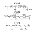
- the voltage control system is formed with the assumption that the inverter and output filter reactor in combination act as an ideal current source, as shown in FIG. 12.
- a redicted value I L * (k) used here is obtained by quadratic prediction (4) shown in the block diagram of FIG. 13.
- the value of G 3 for attaining a finite settlement is obtained.
- the primary feature of this method is the provision of a voltage control system outside of a current control system to form a dual Dead Beat control system. Because of a high response operation realized by Dead Beat control for the voltage control system, voltage deviations induced by the causes which have been itemized in (i) - (iii) can be corrected promptly and a stable control system is realized.
- step T s double period of sampling time T s is adopted for step T of Dead Beat control as explained below.
- the step number of sampling m is used to distinguish from k of discretization of Dead Beat control.
- capacitor Cp is considered to be separated from the load 5, as shown in FIG. 6. But as an another embodiment that capacitor can be thought as one part of load 5, and then in this case, the block 202 for capacitor current command is eliminated and inverter current I A , that is the output of sensor 11 a is given as the feedforward signal instead of load current I L , that is the output of sensor 11 b. Even in this case, same construction of the current minor loop can be adopted. That is, in the procedure to construct current minor loop, Cp is considered explicitly as from equation (1) to equation (11).
- a specific circuit for carrying out the digital sampling control as shown in FIG. 17, comprises a microprocessor system 230 which implements the calculation of the foregoing Dead Beat control, a crystal oscillator 231 as a time base, a counter circuit-A 232 which performs 512 counts, a counter circuit-B 233 which performs 130 counts, sample hold circuits 234, 235 and 236 which sample and hold the voltage Vc, currents I A and I L respectively, a multiplexer 237, an analog-digital (A/D) converter 238, a flip-flop circuit 239, and a comparator 240.
- a microprocessor system 230 which implements the calculation of the foregoing Dead Beat control
- a crystal oscillator 231 as a time base
- a counter circuit-A 232 which performs 512 counts
- a counter circuit-B 233 which performs 130 counts
- sample hold circuits 234, 235 and 236 which sample and hold the voltage Vc, currents I A and I L respectively
- the microprocessor system 230 is composed of a single-chip microprocessor 230A, a crystal oscillator 230B, a latch circuit 230C, a ROM 230D, inverters 230E and 2301, a resistor 230F, a switch 230G, and a Power ON Reset circuit 230H.
- the single-chip microprocessor 230A acts using the crystal oscillator 230B as the system clock connected to the X1 terminal.
- the latch circuit 230C is connected to the port terminal PD7-0 of the address data bus of the microprocessor 230A, and latches the lower 8 bits of the address in response to signal of the ALE terminal.
- the terminal PF5-0 of the port F outputs the upper 6 bits of the address, and when the address is OOOOH-1 FFFH the ROM 230D is accessed.
- the control program is stored in the ROM 230D, and data is read in the single-chip microprocessor 230A in response to signal of the RD terminal.
- the switch 230G is a switch of start/stop operation of the inverters and connected to the pull-up resistor 230F, and the joint is connected to the terminal PB4 of the microprocessor 230A.
- the Power ON Reset circuit 230H is inputted to the RESET terminal, and resets the single-chip microprocessor 230A when the control power source is turned on.
- the counter circuit-A 232 performs the frequency dividing of output from the crystal oscillator 231 as the time base, and generates sawtooth wave signal being the reference value of the pulse width modulation and interrupt signal to determine the sampling time.
- the interrupt signal is inputted to the interrupt terminal INT1 of the single-chip microprocessor 230A, and execution of the control program is started by the interrupt signal.
- the counter circuit-B 233 receives output of the counter circuit-A 232 and further reduces the frequency, and produces the time reference for the sinusoidal wave voltage reference and inputs it as signal of 8 bits to the terminal PA7-0 of the port A of the single-chip microprocessor 230A.
- the counter circuit-A 232 is composed of program counters 232A, 232B and 232C
- the counter circuit-B 233 is composed of program counters 233A and 233B.
- the time base of 3.9936 MHz outputted from the crystal oscillator 231 is frequency-divided by 512 in the counter circuit-A 232, and is further frequency-divided by 130 in the counter circuit-B 233.
- the interrupt signal corresponds to the frequency dividing of the sawtooth wave signal by 2
- the sinusoidal wave output voltage of 60 Hz is controlled by the carrier frequency 15.6 kHz and the sampling frequency 7.8 kHz. That is, since the period of the PWM is 64 u.s being a half of the sampling period 128 us, it is outputted twice in the same pulse width. This is effected so that the carrier frequency is made higher than audio frequency.
- the voltage V e , the currents I A and required for the waveform control are taken by the sample hold circuits 234 - 236.
- the same signal as the interrupt signal inputted to the interrupt terminal INT 1 is supplied commonly to all sample hold circuits 234 - 236.
- These sample hold circuits 234 - 236 act so that value at a moment of the interrupt signal is held during the 1/2 sampling time and sample during the residual 1/2 sampling time.
- Analog signal held in the sample hold circuits 234 - 236 are selected by the multiplexer 237 and converted into digital signals by the A-D converter 238.
- Action of the multiplexer 237 and the A-D converter 238 is controlled by the terminals PBO - PB3 of the port B of the single-chip microprocessor 230A.
- the single-chip microprocessor 230A selects a chip by signal from the terminal PF5 through the inverter 230E, and analog signal is read in the A-D converter 238 by signal from the terminal RD.
- the inverter output voltage command being a calculation result of the single-chip microprocessor 230A is supplied from the terminal PC7-0 of the port C to the latch circuit 239 every sampling time, and compared with the sawtooth wave of counter A by the comparator 240 thereby the PWM signal is obtained.
- process of calculating the control gain by multiplication may be performed only by referring to the DATA-TABLE where the control gain is previously calculated by multiplication, and therefore the actual calculation need not be performed. Also the division by the DC voltage in ST 12 may be performed only by reading the DATA-TABLE so as to avoid the time-consuming calculation.
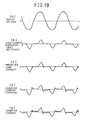
- FIG. 19 shows a set of waveforms at various portions of the system based on the foregoing principle in which the inverter is combined with a capacitor-input rectifier load.
- the distortion of the output voltage is less than 5% for the rectifier load which is the inverter rated kW multiplied by 0.8.
- load current I L can be expressed by equation (20). Then, load current I L can be calculated as the difference of inverter current I A and capacitor current I c . And also capacitor current I e can be estimated from differential calculus of the capacitor voltage V c and multiply it by constant capacitor value Cp.
- load current can be estimated indirectly without load current sensor 11 b.
- a high-frequency inverter 300 has its output through a transformer 303 controlled by a cycloconverter 301 to an arbitrary frequency and it is fed through a filter 302 for shaping to become a sinusoidal waveform before being supplied to a load.
- the inventive control circuit is designed to produce a current command value for a converter to produce a sinusoidal output voltage and to implement instantaneous-value control so that the converted output current follows the current command, with resultant effectiveness including a satisfactory accuracy and transient response of the converted output voltage, a smaller distortion in the output voltage against a harmonic load current, and ensured over-current protection for the switching devices by the current control minor loop against an inrush current or short-circuitting in the load.
- a harmonic load current is controlled on a feed-forward basis, instead of a voltage error feedback correction, whereby production of an accurate voltage and waveform can be accomplished.
Landscapes
- Engineering & Computer Science (AREA)
- Power Engineering (AREA)
- Inverter Devices (AREA)
Claims (12)
eine unterlagerte Stromregelschleife (11 a, 107; 11a, 207), mit der der Augenblickswert des durch die Induktivität (2) fließenden Stromes (I) in Übereinstimmung mit einem Stromreferenzwert (IR; IA *) geregelt wird, der durch folgende Summe folgender Größen gegeben ist:
die Kondensatorstromkomponente (ICR; Ic *) durch eine Rechenschaltung (103; 202) aus einer phasenverschobenen Spannungskomponente (VR90) der sinusförmigen Referenzspannung (VR) abgeleitet wird.
die Laststromkomponente (ILR; IL *) einem vorbestimmten Wert des Laststromes entspricht.
der vorbestimmte Wert des Laststroms durch ein quadratisches Vorhersageverfahren unter Benutzung von derzeitigen und vorhergehenden Lastromwerten ermittelt wird.
die unterlagerte Stromregelschleife ein Abtastdaten-Regelsystem ist.
die Modifikationsstromkomponente (IVR; Ic) durch Abtastdatenregelung unter Benutzung eines finiten Abgleichregelsystems ermittelt wird.
der Umrichter aus einem Wechselrichter (1) besteht, der Gleichstrom in Wechselstrom umwandelt.
die Verstärkungsfaktoren der finiten Abgleichregelung durch eine Diskretisierungszeit T bestimmt werden, die der zweifachen Abtastzeit Ts entspricht.
den Ausgangswert dieser Abtastzeit zu bestimmen, daß nach der Berechnung des Ausgangswertes der Wert VAO(m) dieser Diskretisierungsperiode ermittelt wird und daß der Ausgangswert VA(m + 1 ) der nächsten Abtastzeit der Regelschaltung als
Applications Claiming Priority (6)
| Application Number | Priority Date | Filing Date | Title |
|---|---|---|---|
| JP9119286 | 1986-04-22 | ||
| JP91192/86 | 1986-04-22 | ||
| JP15196286 | 1986-06-27 | ||
| JP151962/86 | 1986-06-27 | ||
| JP8473/87 | 1987-01-17 | ||
| JP62008473A JPH0744841B2 (ja) | 1986-04-22 | 1987-01-17 | 電力変換器の制御回路 |
Publications (3)
| Publication Number | Publication Date |
|---|---|
| EP0243840A2 EP0243840A2 (de) | 1987-11-04 |
| EP0243840A3 EP0243840A3 (en) | 1989-06-07 |
| EP0243840B1 true EP0243840B1 (de) | 1992-12-02 |
Family
ID=27278032
Family Applications (1)
| Application Number | Title | Priority Date | Filing Date |
|---|---|---|---|
| EP87105791A Expired - Lifetime EP0243840B1 (de) | 1986-04-22 | 1987-04-18 | Steuerschaltung für einen Umrichter |
Country Status (3)
| Country | Link |
|---|---|
| US (1) | US4757434A (de) |
| EP (1) | EP0243840B1 (de) |
| DE (1) | DE3782848T2 (de) |
Families Citing this family (45)
| Publication number | Priority date | Publication date | Assignee | Title |
|---|---|---|---|---|
| US5111380A (en) * | 1986-10-10 | 1992-05-05 | Nilssen Ole K | Controlled series-resonance-loaded inverter |
| JPH01152928A (ja) * | 1987-12-09 | 1989-06-15 | Toshiba Corp | 電力変換装置の制御装置 |
| WO1990006621A1 (en) * | 1988-12-05 | 1990-06-14 | Sundstrand Corporation | Vscf start system with precise voltage control |
| US5347441A (en) * | 1989-09-18 | 1994-09-13 | Mitsubishi Denki Kabushiki Kaisha | Thyristor converter system with higher harmonics suppression |
| US4935860A (en) * | 1989-10-13 | 1990-06-19 | Sundstrand Corporation | PWM inverter circuit having modulated DC link input |
| US4937720A (en) * | 1989-10-13 | 1990-06-26 | Sundstrand Corporation | PWM inverter circuit analytically compensating for DC link distortion |
| US4961130A (en) * | 1989-12-11 | 1990-10-02 | Sundstrand Corporation | Voltage inverter control applying real-time angle pattern determination |
| US5043857A (en) * | 1990-04-11 | 1991-08-27 | Sundstrand Corporation | Real-time control of PWM inverters by pattern development from stored constants |
| US4977492A (en) * | 1990-04-25 | 1990-12-11 | Sundstrand Corporation | Suppression of switching harmonics |
| US5053939A (en) * | 1990-08-27 | 1991-10-01 | Sundstrand Corporation | Control of PWM inverters by pattern development from stored constants relating D.C. link harmonics to output distortion |
| US5229929A (en) * | 1990-11-30 | 1993-07-20 | Honda Giken Kogyo Kabushiki Kaisha | Output peak current correction for PWM invertors |
| JP2884880B2 (ja) * | 1992-02-12 | 1999-04-19 | 株式会社日立製作所 | 電力変換器の制御装置 |
| US5343379A (en) * | 1992-11-06 | 1994-08-30 | Sundstrand Corporation | Control method for inverters having dwell times between switch conduction periods |
| JP3022063B2 (ja) * | 1993-01-07 | 2000-03-15 | 三菱電機株式会社 | 電力変換器の制御装置 |
| DE4311896A1 (de) * | 1993-04-10 | 1994-10-20 | Thomas Dipl Ing Loesel | Verfahren zur Bestimmung der Einschaltzeiten der Schalter eines n-phasigen Pulsstromwechselrichters |
| US5452198A (en) * | 1994-02-09 | 1995-09-19 | Sundstrand Corporation | Apparatus and method for A/C voltage sensing |
| US5680302A (en) * | 1995-08-24 | 1997-10-21 | Nippon Steel Corporation | AC output control apparatus |
| JP3245523B2 (ja) * | 1995-10-16 | 2002-01-15 | シャープ株式会社 | インバータ制御方法およびインバータ制御装置 |
| JP3233005B2 (ja) * | 1996-03-01 | 2001-11-26 | 株式会社日立製作所 | Pwm制御装置 |
| US5774351A (en) * | 1996-05-21 | 1998-06-30 | National Science Council | Series resonant DC-to-AC inverter system |
| JP3234909B2 (ja) * | 1996-12-13 | 2001-12-04 | シャープ株式会社 | インバータ制御装置、およびインバータの制御方法 |
| GB2351620A (en) * | 1999-07-01 | 2001-01-03 | Semelab Plc | Triangle wave generator, current sensor, class D power amplifier, anti-hiss circuit and loudspeaker protection circuit |
| KR100325407B1 (ko) * | 1999-07-09 | 2002-03-04 | 이종수 | 펄스폭 변조 제어 시스템 |
| US6960984B1 (en) | 1999-12-08 | 2005-11-01 | University Of North Carolina | Methods and systems for reactively compensating magnetic current loops |
| US6469485B2 (en) | 2000-07-07 | 2002-10-22 | Honeywell International Inc. | Active filter and method for suppressing current harmonics |
| AU2002241795A1 (en) * | 2000-10-27 | 2002-05-27 | Youtility Inc | Inverter dc link volts "tooth" modulation scheme |
| JP4284879B2 (ja) * | 2001-03-19 | 2009-06-24 | 三菱電機株式会社 | 電力変換装置 |
| EP1451814A4 (de) * | 2001-11-15 | 2009-05-06 | Sony Music Entertainment Inc | System und verfahren zur steuerung der benutzung und duplikation von auf wechselbaren medien verteiltem digitalem inhalt |
| US6472775B1 (en) | 2001-11-30 | 2002-10-29 | Ballard Power Systems Corporation | Method and system for eliminating certain harmonics in a distributed power system |
| US8152305B2 (en) | 2004-07-16 | 2012-04-10 | The University Of North Carolina At Chapel Hill | Methods, systems, and computer program products for full spectrum projection |
| JP4742781B2 (ja) * | 2005-09-28 | 2011-08-10 | トヨタ自動車株式会社 | 交流電圧出力装置およびそれを備えたハイブリッド自動車 |
| TWI327812B (en) * | 2006-11-28 | 2010-07-21 | Ind Tech Res Inst | Inverter circuit and control circuit thereof |
| JP4945476B2 (ja) * | 2008-02-20 | 2012-06-06 | オリジン電気株式会社 | 単相電圧型交直変換装置及び三相電圧型交直変換装置 |
| ES2823456T3 (es) | 2009-06-25 | 2021-05-07 | Univ North Carolina Chapel Hill | Método y sistema para utilizar postes unidos a una superficie accionados para evaluar la reología de fluidos biológicos |
| EP2661805B1 (de) | 2011-01-04 | 2019-08-14 | Enphase Energy, Inc. | Verfahren und vorrichtung zur resonanzstromwandlung |
| WO2012162581A1 (en) * | 2011-05-26 | 2012-11-29 | Enphase Energy, Inc. | Method and apparatus for generating single-phase power from a three-phase resonant power converter |
| TWI448065B (zh) * | 2012-01-17 | 2014-08-01 | Univ Nat Chiao Tung | 多相反流器控制裝置及其輸出電流控制方法 |
| US9201446B2 (en) * | 2012-02-01 | 2015-12-01 | Microchip Technology Incorporated | Timebase peripheral |
| JP5803946B2 (ja) * | 2013-01-16 | 2015-11-04 | 株式会社デンソー | スイッチングレギュレータ |
| US9444323B2 (en) * | 2014-01-22 | 2016-09-13 | Solidstate Controls, Llc | Power conversion system having a harmonic distortion limiter |
| CN104035462B (zh) * | 2014-05-30 | 2016-09-28 | 华为技术有限公司 | 一种电源控制方法及设备 |
| WO2017138103A1 (ja) * | 2016-02-10 | 2017-08-17 | 田淵電機株式会社 | 自立運転制御装置、パワーコンディショナ及び自立運転制御方法 |
| US11349410B2 (en) * | 2018-01-30 | 2022-05-31 | Mitsubishi Electric Corporation | Series multiplex inverter |
| CN112803783B (zh) * | 2021-03-17 | 2022-07-26 | 北京动力源科技股份有限公司 | 一种基于数字控制的直流变换器增益调制系统 |
| TWI869003B (zh) * | 2023-10-25 | 2025-01-01 | 國立臺灣大學 | 具有中性線偏置電流補償功能的功率調節器及其控制方法 |
Citations (1)
| Publication number | Priority date | Publication date | Assignee | Title |
|---|---|---|---|---|
| EP0215362A2 (de) * | 1985-09-09 | 1987-03-25 | Kabushiki Kaisha Toshiba | Wechselstromversorgungseinrichtung |
Family Cites Families (8)
| Publication number | Priority date | Publication date | Assignee | Title |
|---|---|---|---|---|
| US3636430A (en) * | 1970-10-26 | 1972-01-18 | Westinghouse Electric Corp | Anticipatory feedback control for inverters |
| US3781634A (en) * | 1971-06-18 | 1973-12-25 | Westinghouse Electric Corp | Integrated error voltage regulator for static switching circuits |
| GB1504313A (en) * | 1974-03-11 | 1978-03-15 | Nippon Telegraph & Telephone | Inverter controlling device |
| US4377779A (en) * | 1980-12-29 | 1983-03-22 | General Electric Company | Pulse width modulated inverter machine drive |
| US4468724A (en) * | 1981-04-08 | 1984-08-28 | Hitachi, Ltd. | Method and apparatus for controlling load current |
| JPS58130792A (ja) * | 1982-01-28 | 1983-08-04 | Fanuc Ltd | 同期電動機の駆動装置 |
| JPS59123478A (ja) * | 1982-12-28 | 1984-07-17 | Toshiba Corp | 電圧形インバ−タの制御装置 |
| US4541041A (en) * | 1983-08-22 | 1985-09-10 | General Electric Company | Full load to no-load control for a voltage fed resonant inverter |
-
1987
- 1987-04-18 EP EP87105791A patent/EP0243840B1/de not_active Expired - Lifetime
- 1987-04-18 DE DE8787105791T patent/DE3782848T2/de not_active Expired - Fee Related
- 1987-04-21 US US07/041,042 patent/US4757434A/en not_active Expired - Lifetime
Patent Citations (1)
| Publication number | Priority date | Publication date | Assignee | Title |
|---|---|---|---|---|
| EP0215362A2 (de) * | 1985-09-09 | 1987-03-25 | Kabushiki Kaisha Toshiba | Wechselstromversorgungseinrichtung |
Also Published As
| Publication number | Publication date |
|---|---|
| EP0243840A2 (de) | 1987-11-04 |
| DE3782848T2 (de) | 1993-04-01 |
| DE3782848D1 (de) | 1993-01-14 |
| EP0243840A3 (en) | 1989-06-07 |
| US4757434A (en) | 1988-07-12 |
Similar Documents
| Publication | Publication Date | Title |
|---|---|---|
| EP0243840B1 (de) | Steuerschaltung für einen Umrichter | |
| Bode et al. | An improved robust predictive current regulation algorithm | |
| US4823251A (en) | Controller for instantaneous output current and/or voltage of 3-phase converter | |
| US5373223A (en) | Power converter/inverter system with instantaneous real power feedback control | |
| US5136494A (en) | Power conversion system with instantaneous real power feedback control | |
| US5880947A (en) | Control device for a PWM controlled converter having a voltage controller | |
| US4529925A (en) | Reactive power compensating cycloconverter | |
| EP0307719B1 (de) | Leistungsquelleneinrichtung | |
| US5359275A (en) | Load current fundamental filter with one cycle response | |
| EP1741178B1 (de) | Stromwandlervorrichtung und verfahren mit einer aus einer gleichstrombusspannung abgeleiteten phasenreferenz | |
| Guerrero et al. | A nonlinear feed-forward control technique for single-phase UPS inverters | |
| JP2924601B2 (ja) | 電力変換装置 | |
| JPH01136568A (ja) | 電力変換装置の制御回路 | |
| JPS63274374A (ja) | 電力変換器の制御回路 | |
| JP3065517B2 (ja) | 多相交流より直流を得る電圧形コンバータの制御装置 | |
| Guo et al. | A Sensorless Current Feedforward Method for Single-Phase AC–DC Converter | |
| JPH0783599B2 (ja) | 循環電流形サイクロコンバ−タの制御方法 | |
| Kim et al. | Digital control scheme of UPS inverter to improve the dynamic response | |
| JP2658620B2 (ja) | 電力変換器の制御回路 | |
| JP3170119B2 (ja) | 電力変換装置 | |
| JP2781602B2 (ja) | 電力変換器の制御装置及びそのシステム | |
| KR900005426B1 (ko) | 인버터 제어회로 | |
| JPH03245793A (ja) | 交流電動機の制御方法及びその装置 | |
| JPS63136968A (ja) | 変換器の制御回路 | |
| JPH06261584A (ja) | 交流電動機の制御装置 |
Legal Events
| Date | Code | Title | Description |
|---|---|---|---|
| PUAI | Public reference made under article 153(3) epc to a published international application that has entered the european phase |
Free format text: ORIGINAL CODE: 0009012 |
|
| AK | Designated contracting states |
Kind code of ref document: A2 Designated state(s): CH DE FR GB LI |
|
| PUAL | Search report despatched |
Free format text: ORIGINAL CODE: 0009013 |
|
| AK | Designated contracting states |
Kind code of ref document: A3 Designated state(s): CH DE FR GB LI |
|
| 17P | Request for examination filed |
Effective date: 19890922 |
|
| 17Q | First examination report despatched |
Effective date: 19891120 |
|
| GRAA | (expected) grant |
Free format text: ORIGINAL CODE: 0009210 |
|
| AK | Designated contracting states |
Kind code of ref document: B1 Designated state(s): CH DE FR GB LI |
|
| REF | Corresponds to: |
Ref document number: 3782848 Country of ref document: DE Date of ref document: 19930114 |
|
| ET | Fr: translation filed | ||
| PLBE | No opposition filed within time limit |
Free format text: ORIGINAL CODE: 0009261 |
|
| STAA | Information on the status of an ep patent application or granted ep patent |
Free format text: STATUS: NO OPPOSITION FILED WITHIN TIME LIMIT |
|
| 26N | No opposition filed | ||
| REG | Reference to a national code |
Ref country code: GB Ref legal event code: IF02 |
|
| PGFP | Annual fee paid to national office [announced via postgrant information from national office to epo] |
Ref country code: FR Payment date: 20040408 Year of fee payment: 18 |
|
| PGFP | Annual fee paid to national office [announced via postgrant information from national office to epo] |
Ref country code: GB Payment date: 20040414 Year of fee payment: 18 |
|
| PGFP | Annual fee paid to national office [announced via postgrant information from national office to epo] |
Ref country code: CH Payment date: 20040416 Year of fee payment: 18 |
|
| PGFP | Annual fee paid to national office [announced via postgrant information from national office to epo] |
Ref country code: DE Payment date: 20040429 Year of fee payment: 18 |
|
| PG25 | Lapsed in a contracting state [announced via postgrant information from national office to epo] |
Ref country code: GB Free format text: LAPSE BECAUSE OF NON-PAYMENT OF DUE FEES Effective date: 20050418 |
|
| PG25 | Lapsed in a contracting state [announced via postgrant information from national office to epo] |
Ref country code: LI Free format text: LAPSE BECAUSE OF NON-PAYMENT OF DUE FEES Effective date: 20050430 Ref country code: CH Free format text: LAPSE BECAUSE OF NON-PAYMENT OF DUE FEES Effective date: 20050430 |
|
| PG25 | Lapsed in a contracting state [announced via postgrant information from national office to epo] |
Ref country code: DE Free format text: LAPSE BECAUSE OF NON-PAYMENT OF DUE FEES Effective date: 20051101 |
|
| REG | Reference to a national code |
Ref country code: CH Ref legal event code: PL |
|
| GBPC | Gb: european patent ceased through non-payment of renewal fee |
Effective date: 20050418 |
|
| PG25 | Lapsed in a contracting state [announced via postgrant information from national office to epo] |
Ref country code: FR Free format text: LAPSE BECAUSE OF NON-PAYMENT OF DUE FEES Effective date: 20051230 |
|
| REG | Reference to a national code |
Ref country code: FR Ref legal event code: ST Effective date: 20051230 |