EP0217043A1 - Dispositif de détection d'erreurs dans le circuit de chauffage d'une tête d'impression thermique - Google Patents
Dispositif de détection d'erreurs dans le circuit de chauffage d'une tête d'impression thermique Download PDFInfo
- Publication number
- EP0217043A1 EP0217043A1 EP86110319A EP86110319A EP0217043A1 EP 0217043 A1 EP0217043 A1 EP 0217043A1 EP 86110319 A EP86110319 A EP 86110319A EP 86110319 A EP86110319 A EP 86110319A EP 0217043 A1 EP0217043 A1 EP 0217043A1
- Authority
- EP
- European Patent Office
- Prior art keywords
- circuit
- print head
- heating
- fault detection
- photocoupler
- Prior art date
- Legal status (The legal status is an assumption and is not a legal conclusion. Google has not performed a legal analysis and makes no representation as to the accuracy of the status listed.)
- Granted
Links
Images


Classifications
-
- B—PERFORMING OPERATIONS; TRANSPORTING
- B41—PRINTING; LINING MACHINES; TYPEWRITERS; STAMPS
- B41J—TYPEWRITERS; SELECTIVE PRINTING MECHANISMS, i.e. MECHANISMS PRINTING OTHERWISE THAN FROM A FORME; CORRECTION OF TYPOGRAPHICAL ERRORS
- B41J2/00—Typewriters or selective printing mechanisms characterised by the printing or marking process for which they are designed
- B41J2/315—Typewriters or selective printing mechanisms characterised by the printing or marking process for which they are designed characterised by selective application of heat to a heat sensitive printing or impression-transfer material
- B41J2/32—Typewriters or selective printing mechanisms characterised by the printing or marking process for which they are designed characterised by selective application of heat to a heat sensitive printing or impression-transfer material using thermal heads
- B41J2/35—Typewriters or selective printing mechanisms characterised by the printing or marking process for which they are designed characterised by selective application of heat to a heat sensitive printing or impression-transfer material using thermal heads providing current or voltage to the thermal head
Definitions
- This invention relates to a thermal print head heating circuit fault detection device, and particularly to a device circuit configuration which is simple and which can perform detection stably at high speed.
- the print heads used in thermal printers are provided with a plurality of heating circuits, each of which is provided with heating elements, gate circuits, transistors, and so forth.
- the heating circuits will not function if a heating element, gate circuit or transistor fails, which will therefore cause part of a dot raster to be output with the printing in a non-functional state. The most frequent cause of such failure is circuit line breakage in the heating elements.
- the object of the present invention is to provide a thermal print head heating circuit fault detection device which has a simple circuit configuration, does not need adjustment even when there exists manufacturing error in the resistance values of the heating elements, and which can perform high-speed detection of circuit faults with high reliability.
- the present invention comprises providing between the print head possessing the heating circuits and the power supply circuit of the print head a required number of diodes connected in series to form a constant voltage circuit, a photocoupler arranged so that the emitter of the photocoupler is driven by the difference in the potentials arising between the two ends of the diodes, and a control circuit which applies a sequential electrical condition to the heating circuits of the print head and checks the output of the photocoupler collector to thereby perform detection of heating circuit faults.
- a program ROM 31 connected to a CPU 30 are a program ROM 31, a data RAM 32 and an I/O port 33.
- the CPU 30 performs overall control of printer functions, such as printing and heating circuit fault detection, in accordance with a program stored in the program ROM 31.
- Stored in the data RAM 32 are printing data, the location of faulty heating circuits determined on the basis of the results of heating circuit fault detection, and the like.
- a print data input circuit 34 for the input of the data to be printed
- a drive circuit 35 for driving a pulse motor 36 used to transport the printing paper
- a drive circuit 37 for driving a display 38, such as a CRT
- a drive circuit 39 for driving a buzzer 40
- a thermal print head 41 is also connected to the I/O port 33 so that on the one hand it supplies power directly to the print head 41 and on the other hand it supplies power to the print head through a fault detection circuit 42.
- This fault detection circuit 42 and power supply circuit 43 are each connected to the I/O port 33 so as to be suitably controlled by the CPU 30 in accordance with the program.
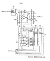
- Fig. 2 shows details of the print head 41, the fault detection circuit 42 and the power supply circuit 43.
- the print head 41 is provided with a data register 44 comprised of shift registers, a latch circuit 45 and n heating circuits S1, S2, S3, ..., S n .
- Each of the heating circuits S1, S2, S3, ..., S n is comprised of AND gates G1, G2, G3, ..., G n , transistors Tr1, Tr2, Tr3, ..., Tr n , and heating elements R1, R2, R3, ..., R n .
- the data register 44 is for storing one dot-line of printing data, the data input DI being input one bit at a time via I/O port 33 by means of a clock signal CLK and output to the latch circuit 45.
- the latch circuit 45 is arranged so that when a latch signal LAT is input via the I/O port 33 the data stored in the data register 44 is read out.
- the output terminals of the latch circuit 45 are connected to one of the input terminals of the AND gates G1, G2, G3, ..., G n .
- the other input terminal of each of the AND gates G1, G2, G3, ..., G n is connected to the input terminal of the I/O port 33 for the input of a strobe signal STR.
- the output terminal of each of the AND gates G1, G2, G3, ..., G n is connected to the base of the corresponding transistor Tr1, Tr2, Tr3, ..., Tr n .
- the emitter of each of the transistors Tr1, Tr2, Tr3, ..., Tr n is grounded, and the collector is connected to one side of the corresponding heating element R1, R2, R3, ..., R n .
- each of the heating elements R1, R2, R3, ..., R n is connected to a common terminal 46 of the print head 41.
- the power supply circuit 43 is provided with two power supplies each having the same voltage. Power supply P is for printing operations and is supplied directly to the common terminal 46 of the print head 41 via a diode D4, while power supply C is for fault detection purposes and is connected to the common terminal 46 of the print head 41 via the fault detection circuit 42.
- the fault detection circuit 42 consisting of diodes D1, D2 and D3, fixed resistances R a and R b , a variable resistance VR, and the photocoupler 47 will now be described.
- the diodes D1, D2 and D3 are silicon diodes connected in series in that order between the power supply circuit 43 and the print head 41.
- Connected to the anode side of the diode D1 is the variable resistance VR, and connected to the variable resistance VR is the fixed resistance R a .
- Connected between the fixed resistance R a and the cathode side of the diode D3 is a photodiode PD that forms the emitter portion of the photocoupler 47. That is, a circuit consisting of the variable resistance VR, the fixed resistance R a and the photodiode PD of the photocoupler 47 is connected in parallel with the diodes D1, D2 and D3 which are connected in series.
- the voltage reduction produced by the said three diodes D1, D2 and D3 connected in series is constant. Therefore, as the diodes D1, D2 and D3 form a constant voltage circuit, the voltage between point A and point B remains constant.
- fault detection power supply C is now supplied, a prescribed voltage is produced between point A and point B, there is a flow of current in the variable resistance VR, the fixed resistance R a and the photodiode PD, and the photodiode PD lights.
- the number of diodes is not limited to three, but may be any number that is sufficient to produce enough of a voltage drop to cause the photodiode PD to light.
- the variable resistance VR is provided for adjusting the value of the current flow through the photodiode PD.
- the emitter of the phototransistor PTr which forms the collector of the photocoupler 47 is grounded and the collector is connected to the power source via resistor R b .
- the collector of the phototransistor PTr is also connected to the I/O port 33, and the CPU 30 performs the detection of faults in the heating circuits S1, S2, S3, ..., S n by detecting the potential of the said collector.
- the fault detection power supply C comes from the power supply circuit 43, it goes to the print head 41 via the fault detection circuit 42, but if there is any fault in the heating circuits S1, S2, S3, ..., S n that are the object of the detection process, there will be no difference in potential produced between point A and point B, and hence no emission by the photodiode PD, and accordingly, the collector side of the phototransistor PTr goes High. Again, if there is no fault a potential difference will be produced between point A and point B, the photodiode PD lights, and the collector side of the phototransistor PTr goes Low. If the CPU 30 which is monitoring the phototransistor PTr collector potential detects that the potential has gone High, the CPU 30 determines that a circuit fault has occurred, while if the potential is Low the circuit is determined to be normal.
- step 1 the number of heating circuits S1, S2, S3, ..., S n , that is, the total number of dots N of the print head 41, is placed into a specific address of the data RAM 32.
- step 2 by turning off printing power supply P and turning on fault detection power supply C, power is supplied to the common terminal 46 of the print head 41 via the fault detection circuit 42.
- step 3 by inputting a single clock signal CLK with the input data DI in the High state, a binary "1" signal is set into the first stage of the data register 44.
- a latch signal LAT is input to latch the contents of the data register 44 with the latch circuit 45, and a strobe signal STR is input to obtain a current flow only in heating circuit S1.
- the collector-side potential of the phototransistor PTr is checked, and if it is Low, it is determined that the heating circuit S1 is normal, while if it is High it is determined that it is faulty. That is, when heating circuit S1 is in a faulty condition owing to a circuit line break or the like in the heating element R1, current does not flow in the heating circuit S1 or the fault detection circuit 42, so no difference in potential between point A and point B is produced.
- the heating circuit S1 When the heating circuit S1 is working normally, current flows through the fault detection circuit 42 to the heating circuits, producing a potential difference between point A and point B, so there is emission by the photodiode PD and the collector-side potential of the phototransistor PTr goes Low.
- the pulse of the strobe signal STR is set to a narrow enough width that the heating elements R1, R2, R3, ..., R n do not print.
- step 7 a value N corresponding to the number of the faulty heating circuit is stored in a specific address of the data RAM 32, after which the N value is decremented by just one in step 8.
- step 9 by inputting a single clock signal CLK with the input data DI of the data register 44 in the Low state, the binary "1" signal is shifted from the first to the second position of the data register 44.
- step 10 it is determined whether N equals zero or not.
- step 4 If N does not equal zero it is determined that checking of all of the heating circuits S1, S2, S3, ..., S n has not yet been completed, and the procedures of step 4 through step 10 are repeated.
- N By applying an electrical condition in sequence to each of the heating elements S1, S2, S3, ..., S n and also checking the collector-side potential of the phototransistor PTr, when the checking for circuit faults has thus been completed for all of the heating circuits S1, S2, S3, ..., S n , N becomes zero and the process advances to step 11.
- step 11 it is determined whether there is a faulty heating circuit. If it is determined that there is no faulty heating circuit, the print head 41 heating circuit fault detection operation is terminated and printing or other such operations are proceeded with. When it is determined that there is a faulty heating circuit, reference is made to the faulty heating circuit number stored in the data RAM 32 to determine the extent of the fault in terms of printing capability, i.e. whether printing is possible. Then, in step 13, the display 38 is used to indicate whether printing is possible and also to show the number of the faulty heating circuit or circuits, and a buzzer sounds to signal the completion of the heating circuit fault detection operation.
- the printing operation does not form part of the gist of the present invention, details thereof will be omitted, other than to say that after printing power supply P is turned on and fault detection power supply C is turned off, printing proceeds as the print data is input into the data register 44.
- the pulse of the strobe signal STR is set to a wide enough width to permit printing by the heating elements R1, R2, R3, ..., R n .
- the fault detection power supply C and the printing power supply P are provided as separate circuits, the fault detection power supply C may be utilized for printing in addition to fault detection. Even if such a dual-purpose power supply is employed, the voltage drop in the fault detection circuit 42 during printing remains roughly constant regardless of the number of heating elements R1, R2, R3, ..., R n , so there is no destruction or the like of the photocoupler 47 and printing is not affected.
- the pulse of the strobe signal STR is set to a narrow enough width that printing does not take place
- the pulses of the strobe signal STR may also be set to a width that is the same for both printing and fault detection, with the fault detection power supply C being set to such a value that printing will not take place.
- the present invention comprises providing between the print head possessing the heating circuits and the power supply circuit of the print head a required number of diodes connected in series to form a constant voltage circuit and a photocoupler arranged so that the emitter of the photocoupler is driven by the difference in the potentials arising between the two ends of the diodes, and a control circuit which applies a sequential electrical condition to the heating circuits of the print head and checks the output of the photocoupler collector to thereby perform detection of heating circuit faults.
Landscapes
- Accessory Devices And Overall Control Thereof (AREA)
- Electronic Switches (AREA)
Applications Claiming Priority (2)
| Application Number | Priority Date | Filing Date | Title |
|---|---|---|---|
| JP60202542A JPS6262776A (ja) | 1985-09-14 | 1985-09-14 | サ−マル印字ヘツドの発熱回路不良検出装置 |
| JP202542/85 | 1985-09-14 |
Publications (2)
| Publication Number | Publication Date |
|---|---|
| EP0217043A1 true EP0217043A1 (fr) | 1987-04-08 |
| EP0217043B1 EP0217043B1 (fr) | 1990-07-18 |
Family
ID=16459226
Family Applications (1)
| Application Number | Title | Priority Date | Filing Date |
|---|---|---|---|
| EP86110319A Expired - Lifetime EP0217043B1 (fr) | 1985-09-14 | 1986-07-25 | Dispositif de détection d'erreurs dans le circuit de chauffage d'une tête d'impression thermique |
Country Status (4)
| Country | Link |
|---|---|
| US (1) | US4774526A (fr) |
| EP (1) | EP0217043B1 (fr) |
| JP (1) | JPS6262776A (fr) |
| DE (2) | DE217043T1 (fr) |
Cited By (4)
| Publication number | Priority date | Publication date | Assignee | Title |
|---|---|---|---|---|
| DE3825232C1 (en) * | 1988-07-25 | 1990-02-15 | Nixdorf Computer Ag, 4790 Paderborn, De | Method and circuit arrangement for producing information on the type of a print head |
| EP0605122A2 (fr) * | 1992-12-07 | 1994-07-06 | Pitney Bowes Inc. | Système de timbrage avec signes à selectionner pour compenser les fautes de frappe détectées |
| EP0902385A2 (fr) * | 1997-09-15 | 1999-03-17 | Monarch Marking Systems, INC. | Système de prédiction anticipée de panne d'une tête d'imprimante thermique |
| EP2360022A1 (fr) * | 2008-12-12 | 2011-08-24 | Shandong New Beiyang Information Technology Co., Ltd. | Dispositif et procédé de détection de tête d'impression thermique et imprimante thermique les utilisant |
Families Citing this family (23)
| Publication number | Priority date | Publication date | Assignee | Title |
|---|---|---|---|---|
| JP2731003B2 (ja) * | 1988-12-06 | 1998-03-25 | キヤノン株式会社 | 液体噴射記録装置 |
| US4996487A (en) * | 1989-04-24 | 1991-02-26 | International Business Machines Corporation | Apparatus for detecting failure of thermal heaters in ink jet printers |
| JPH03146360A (ja) * | 1989-10-31 | 1991-06-21 | Kanzaki Paper Mfg Co Ltd | サーマルヘッド断線検知回路 |
| US5072235A (en) * | 1990-06-26 | 1991-12-10 | Xerox Corporation | Method and apparatus for the electronic detection of air inside a thermal inkjet printhead |
| US5675370A (en) * | 1993-11-22 | 1997-10-07 | Intermec Corporation | Printhead having multiple print lines, and method and apparatus for using same |
| US5815179A (en) * | 1995-04-12 | 1998-09-29 | Eastman Kodak Company | Block fault tolerance in integrated printing heads |
| US20040221844A1 (en) * | 1997-06-17 | 2004-11-11 | Hunt Peter John | Humidity controller |
| US10130787B2 (en) | 1997-06-17 | 2018-11-20 | Fisher & Paykel Healthcare Limited | Humidity controller |
| JP3068549B2 (ja) * | 1998-03-05 | 2000-07-24 | 日本電気データ機器株式会社 | サーマルプリンタ |
| US6520615B1 (en) * | 1999-10-05 | 2003-02-18 | Hewlett-Packard Company | Thermal inkjet print head with integrated power supply fault protection circuitry for protection of firing circuitry |
| DE10057360C2 (de) * | 2000-11-18 | 2003-10-23 | Danfoss As | Verfahren zum Überprüfen eines Heizungssystems |
| US6481814B2 (en) | 2001-02-28 | 2002-11-19 | Lemark International, Inc. | Apparatus and method for ink jet printhead voltage fault protection |
| US6735496B1 (en) * | 2001-10-19 | 2004-05-11 | Chromalox, Inc. | System and method of monitoring multiple control loops in a heater system |
| US6758547B2 (en) | 2002-07-10 | 2004-07-06 | Lexmark International, Inc. | Method and apparatus for machine specific overcurrent detection |
| US20040085379A1 (en) * | 2002-11-04 | 2004-05-06 | Matthew Taylor | Self-contained printing device diagnostics |
| CN100528570C (zh) * | 2004-04-16 | 2009-08-19 | 深圳赛意法微电子有限公司 | 喷墨打印机的笔和笔故障检查电路及检查笔中故障的方法 |
| JP4933057B2 (ja) * | 2005-05-13 | 2012-05-16 | キヤノン株式会社 | ヘッド基板、記録ヘッド、及び記録装置 |
| US7635174B2 (en) * | 2005-08-22 | 2009-12-22 | Lexmark International, Inc. | Heater chip test circuit and methods for using the same |
| US7547087B2 (en) * | 2007-02-23 | 2009-06-16 | International Business Machines Corporation | Fault detection circuit for printers with multiple print heads |
| US8220896B2 (en) * | 2009-03-17 | 2012-07-17 | Xerox Corporation | Printhead de-prime system and method for solid ink systems |
| GB2482139B (en) * | 2010-07-20 | 2014-08-13 | Markem Imaje Ltd | Method of testing the health of a heating element of a thermal print head |
| US9022499B2 (en) * | 2011-04-07 | 2015-05-05 | Canon Kabushiki Kaisha | Printing apparatus |
| JP6750304B2 (ja) * | 2016-05-24 | 2020-09-02 | セイコーエプソン株式会社 | サーマルプリンター、及び、サーマルプリンターの制御方法 |
Citations (2)
| Publication number | Priority date | Publication date | Assignee | Title |
|---|---|---|---|---|
| US4500893A (en) * | 1983-04-28 | 1985-02-19 | Tokyo Electric Co., Ltd. | Thermal-printing device with defective resistive heating element detection mode |
| EP0174751A1 (fr) * | 1984-08-14 | 1986-03-19 | Ncr Canada Ltd - Ncr Canada Ltee | Appareil et méthode pour la détermination automatique d'éléments thermiques détecteurs dans une tête d'impression |
Family Cites Families (4)
| Publication number | Priority date | Publication date | Assignee | Title |
|---|---|---|---|---|
| US4207517A (en) * | 1977-06-20 | 1980-06-10 | Bloxam James M | Switchless D.C. multifunction tester |
| US4220912A (en) * | 1977-07-20 | 1980-09-02 | Dana Corporation | Vehicle speed control circuit tester |
| JPS6023060A (ja) * | 1983-07-19 | 1985-02-05 | Tokyo Electric Co Ltd | サ−マルプリンタのヘツド切れ検出装置 |
| US4573058A (en) * | 1985-05-24 | 1986-02-25 | Ncr Canada Ltd - Ncr Canada Ltee | Closed loop thermal printer for maintaining constant printing energy |
-
1985
- 1985-09-14 JP JP60202542A patent/JPS6262776A/ja active Pending
-
1986
- 1986-07-25 DE DE198686110319T patent/DE217043T1/de active Pending
- 1986-07-25 DE DE8686110319T patent/DE3672732D1/de not_active Expired - Lifetime
- 1986-07-25 EP EP86110319A patent/EP0217043B1/fr not_active Expired - Lifetime
- 1986-09-11 US US06/906,230 patent/US4774526A/en not_active Expired - Lifetime
Patent Citations (2)
| Publication number | Priority date | Publication date | Assignee | Title |
|---|---|---|---|---|
| US4500893A (en) * | 1983-04-28 | 1985-02-19 | Tokyo Electric Co., Ltd. | Thermal-printing device with defective resistive heating element detection mode |
| EP0174751A1 (fr) * | 1984-08-14 | 1986-03-19 | Ncr Canada Ltd - Ncr Canada Ltee | Appareil et méthode pour la détermination automatique d'éléments thermiques détecteurs dans une tête d'impression |
Cited By (7)
| Publication number | Priority date | Publication date | Assignee | Title |
|---|---|---|---|---|
| DE3825232C1 (en) * | 1988-07-25 | 1990-02-15 | Nixdorf Computer Ag, 4790 Paderborn, De | Method and circuit arrangement for producing information on the type of a print head |
| EP0605122A2 (fr) * | 1992-12-07 | 1994-07-06 | Pitney Bowes Inc. | Système de timbrage avec signes à selectionner pour compenser les fautes de frappe détectées |
| EP0605122A3 (en) * | 1992-12-07 | 1994-09-21 | Pitney Bowes Inc | Postage metering system with indicia selectable to compensate for detected printer defects. |
| EP0902385A2 (fr) * | 1997-09-15 | 1999-03-17 | Monarch Marking Systems, INC. | Système de prédiction anticipée de panne d'une tête d'imprimante thermique |
| EP0902385A3 (fr) * | 1997-09-15 | 2002-01-09 | Monarch Marking Systems, INC. | Système de prédiction anticipée de panne d'une tête d'imprimante thermique |
| EP2360022A1 (fr) * | 2008-12-12 | 2011-08-24 | Shandong New Beiyang Information Technology Co., Ltd. | Dispositif et procédé de détection de tête d'impression thermique et imprimante thermique les utilisant |
| EP2360022A4 (fr) * | 2008-12-12 | 2013-06-26 | Shandong New Beiyang Inf Tech | Dispositif et procédé de détection de tête d'impression thermique et imprimante thermique les utilisant |
Also Published As
| Publication number | Publication date |
|---|---|
| DE217043T1 (de) | 1987-08-13 |
| JPS6262776A (ja) | 1987-03-19 |
| EP0217043B1 (fr) | 1990-07-18 |
| US4774526A (en) | 1988-09-27 |
| DE3672732D1 (de) | 1990-08-23 |
Similar Documents
| Publication | Publication Date | Title |
|---|---|---|
| EP0217043A1 (fr) | Dispositif de détection d'erreurs dans le circuit de chauffage d'une tête d'impression thermique | |
| EP0217044B1 (fr) | Dispositif pour la détection d'erreurs dans le circuit de chauffage pour tête d'impression thermique | |
| US6120125A (en) | Technique for testing the driving of nozzles in an ink-jet printer | |
| EP0124073B1 (fr) | Imprimante thermique | |
| EP0144016B1 (fr) | Imprimante matricielle par points | |
| EP0072224B1 (fr) | Dispositif de contrôle du circuit d'impression d'une imprimante thermique | |
| KR0167406B1 (ko) | 서멀 헤드 장치 | |
| JP2901032B2 (ja) | Ledプリントヘッド | |
| US4951235A (en) | Option unit detecting apparatus for electronic equipment | |
| JPH01249366A (ja) | サーマル記録装置 | |
| JPH06191079A (ja) | サーマル印字ヘッドの発熱回路不良検出装置 | |
| JP2002137424A (ja) | サーマルヘッドの判別装置および判別方法 | |
| US6402286B1 (en) | Function test device for optical print head heaters in thermal bubble printers | |
| JPS6092875A (ja) | サ−マルプリンタ | |
| JP4592896B2 (ja) | サーマルヘッドの断線チェック装置 | |
| KR0155256B1 (ko) | 잉크젯 프린터의 노즐 검사 방법 | |
| JPH07115483B2 (ja) | サ−マルプリンタの印刷不良検出方法 | |
| JPS59109381A (ja) | インパクトプリンタの異常検出回路 | |
| JPH05104763A (ja) | サーマルプリンタのドツト検査装置 | |
| KR100489181B1 (ko) | 비드(bead)를이용한잉크젯프린터의이상노즐검출회로 | |
| KR100205748B1 (ko) | 잉크젯프린터의 에러노즐 발생시 프린팅의 보상방법 | |
| JPH047711B2 (fr) | ||
| JPS6092876A (ja) | サ−マルプリンタ | |
| JP2954049B2 (ja) | サーマルヘッド | |
| JPH0326664B2 (fr) |
Legal Events
| Date | Code | Title | Description |
|---|---|---|---|
| PUAI | Public reference made under article 153(3) epc to a published international application that has entered the european phase |
Free format text: ORIGINAL CODE: 0009012 |
|
| AK | Designated contracting states |
Kind code of ref document: A1 Designated state(s): DE FR GB |
|
| EL | Fr: translation of claims filed | ||
| 17P | Request for examination filed |
Effective date: 19870604 |
|
| DET | De: translation of patent claims | ||
| 17Q | First examination report despatched |
Effective date: 19880811 |
|
| GRAA | (expected) grant |
Free format text: ORIGINAL CODE: 0009210 |
|
| AK | Designated contracting states |
Kind code of ref document: B1 Designated state(s): DE FR GB |
|
| REF | Corresponds to: |
Ref document number: 3672732 Country of ref document: DE Date of ref document: 19900823 |
|
| ET | Fr: translation filed | ||
| PLBE | No opposition filed within time limit |
Free format text: ORIGINAL CODE: 0009261 |
|
| STAA | Information on the status of an ep patent application or granted ep patent |
Free format text: STATUS: NO OPPOSITION FILED WITHIN TIME LIMIT |
|
| 26N | No opposition filed | ||
| REG | Reference to a national code |
Ref country code: GB Ref legal event code: IF02 |
|
| PGFP | Annual fee paid to national office [announced via postgrant information from national office to epo] |
Ref country code: GB Payment date: 20050701 Year of fee payment: 20 |
|
| PGFP | Annual fee paid to national office [announced via postgrant information from national office to epo] |
Ref country code: FR Payment date: 20050713 Year of fee payment: 20 |
|
| PGFP | Annual fee paid to national office [announced via postgrant information from national office to epo] |
Ref country code: DE Payment date: 20050830 Year of fee payment: 20 |
|
| PG25 | Lapsed in a contracting state [announced via postgrant information from national office to epo] |
Ref country code: GB Free format text: LAPSE BECAUSE OF EXPIRATION OF PROTECTION Effective date: 20060724 |
|
| REG | Reference to a national code |
Ref country code: GB Ref legal event code: PE20 |