EP0124073B1 - Imprimante thermique - Google Patents
Imprimante thermique Download PDFInfo
- Publication number
- EP0124073B1 EP0124073B1 EP84104620A EP84104620A EP0124073B1 EP 0124073 B1 EP0124073 B1 EP 0124073B1 EP 84104620 A EP84104620 A EP 84104620A EP 84104620 A EP84104620 A EP 84104620A EP 0124073 B1 EP0124073 B1 EP 0124073B1
- Authority
- EP
- European Patent Office
- Prior art keywords
- current
- thermal
- printing device
- heat generating
- current path
- Prior art date
- Legal status (The legal status is an assumption and is not a legal conclusion. Google has not performed a legal analysis and makes no representation as to the accuracy of the status listed.)
- Expired
Links
Images


Classifications
-
- B—PERFORMING OPERATIONS; TRANSPORTING
- B41—PRINTING; LINING MACHINES; TYPEWRITERS; STAMPS
- B41J—TYPEWRITERS; SELECTIVE PRINTING MECHANISMS, i.e. MECHANISMS PRINTING OTHERWISE THAN FROM A FORME; CORRECTION OF TYPOGRAPHICAL ERRORS
- B41J2/00—Typewriters or selective printing mechanisms characterised by the printing or marking process for which they are designed
- B41J2/315—Typewriters or selective printing mechanisms characterised by the printing or marking process for which they are designed characterised by selective application of heat to a heat sensitive printing or impression-transfer material
- B41J2/32—Typewriters or selective printing mechanisms characterised by the printing or marking process for which they are designed characterised by selective application of heat to a heat sensitive printing or impression-transfer material using thermal heads
- B41J2/35—Typewriters or selective printing mechanisms characterised by the printing or marking process for which they are designed characterised by selective application of heat to a heat sensitive printing or impression-transfer material using thermal heads providing current or voltage to the thermal head
Definitions
- the present invention relates to a thermal-printing device in accordance to the preamble of claim 1.
- Thermal-printing devices are generally divided into two types; those which print on a heat sensitive paper sheet and those which print on a paper sheet through an ink ribbon coated with a thermally melting ink.
- a thermal-printing device of either type can print clearer data than a line printer or the like.
- heat generating elements can be formed at a finer pitch, which results in printing at a resolution as high as 8 dots/mm. Therefore, a thermal-printing device can print fine images including characters or halftone portions with high quality reproduction characteristics.
- thermal-printing devices are being used not only in the field of OA equipment such as in facsimile systems but also in the field of bar code printing.
- a bar code is used to express a number having a plurality of digits in a form such that each digit has 7 modules in accordance with a relevant standard such as the Japanese Article Numbering system (JAN), the Universal Product Code (UPC), and the European Article Numbering system (EAN).
- JAN Japanese Article Numbering system
- UPC Universal Product Code
- EAN European Article Numbering system
- the 7 modules of a digit "5" including an odd parity, for example, are expressed by "0110001" (where "1" represents black).
- Each module corresponds to a width of 0.33 mm if the magnification factor is 1.
- a standard version is formed of 13 digits for each such number, each digit being expressed by 7 modules. The standard version is read by a laser scanner or the like and is registered in a register.
- Fig 1 shows a conventional thermal-printing device.
- the thermal-printing device has 256 resistors or heat generating elements R1 to R256, and 256 diodes D1 to D256 each having its anode connected to the one terminal of a corresponding resistor.
- these resistors R1 to R256 and diodes D1 to D256 are divided into eight groups. Thus, each group includes 32 resistors and 32 diodes.
- the other terminal of each of the resistors R1 to R32 and R225 to 256 in the first and eighth groups is connected to a common node and thence to a power supply terminal VC through a pnp transistor TR1.
- each of the resistors R33 to R64 and R193 to R224 of the second and seventh groups is connected to a common node and thence to the power supply terminal VC through a pnp transistor TR2.
- the other terminal of each of the resistors R65 to R96 and R161 to R192 of the third and sixth groups, and the other terminal of each of the resistors R97 to R128 and R129 to R160 of the fourth and fifth groups are connected to corresponding common nodes and thence to the power supply terminal VC through respective pnp transistors TR3 and TR4.
- the thermal-printing device shown in Fig. 1 further has a data generator 1 for generating timing signals and printing data, a common electrode selection circuit 2 which controls the conduction state of the transistors TR1 to TR4 in response to the timing signals from the data generator 1, and latch circuits 3 and 4 which latch first and second printing data, respectively, from the data generator 1.
- the latch circuit 3 has first to 32nd output terminals which are respectively connected to the cathodes of the first to 32nd diodes of each of the first to fourth groups of diodes.
- the latch circuit 4 has first to 32nd output terminals which are respectively connected to the cathodes of the first to 32nd diodes of each of the fifth to eighth groups of diodes.
- the data generator 1 includes a data processor which generates a timing signal at a predetermined interval and generates the first and second printing data stored in a memory.
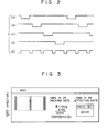
- the selection circuit 2 supplies the selection signals shown in Figs. 2(A) to 2(D) to the transistors TR1 to TR4 so as to sequentially turn them on.
- a low-level signal is supplied to the base of the transistor TR1, for example, the transistor TR1 is turned on.
- a power supply voltage is supplied to the resistors R1 to R32 and R225 to R256 of the first and eighth groups through the transistor TR1.
- a current flows through selected ones of the resistors R1 to R32 and R225 to R256 corresponding to those of the diodes D1 to D32 and D225 to D256 which are selected in accordance with the printing data stored in the latch circuits 3 and 4, as shown in Fig. 2(E).
- the selected resistors are heated.
- a similar operation is repeated and the data stored in the latch circuits 3 and 4 is sequentially printed on a recording paper sheet.
- the recording paper sheet is fed in a predetermined direction to make a label on which the item name, price, weight and the like are printed, as shown in Fig. 3.
- thermo-printing device having heat generating elements, a first current path connected between heat generating elements and power source terminal, a second current path and current detecting means for detecting a current flowing through the second current path.
- the said heat generating elements are not connected to power source terminal through the second current path.
- a thermal-printing device is known (IBM Technical Disclosure Bulletin, Vol. 23, No. 1,p.145,146, June 1980) having current limiting means, first current paths connected to transistors, second current paths connected to transistors and heat generating elements.
- each of the second current paths is connected to a different one of heat generating elements. The device is tested to determine whether or not drive transistors operate and whether or not electrodes contact recording paper.
- the object of the present invention can be achieved by a thermal-printing device in accordance to claim 1.
- the current when a current sequentially flows to the heat generating elements in a check mode, the current is suppressed below a predetermined value by means of a current-limiting element. Therefore, no adverse effect acts on the recording paper sheet.
- a print stop signal is generated by the current detection circuit. Therefore, a broken down element can be checked without adversely affecting the printing operation.
- Fig. 4 is a circuit diagram showing a thermal-printing device according to an embodiment of the present invention.
- the thermal-printing device of this embodiment has pnp transistors TR1 to TR4, resistors R1 to R128, and diodes D1 to D128 having anodes connected to the corresponding resistors R1 to R128.
- the thermal-printing device of this embodiment further has breakdown detector circuits 10-1 to 10-4 which are respectively connected to the first to fourth resistor groups R1 to R32, R33 to R64, R65 to R96 and R97 to R128 and which detect whether the corresponding resistor groups are cut off; a control circuit 12 which has a data generating section 12-1 for generating timing signals and printing data and a check signal generating section 12-2 for generating a check signal CKS and a clock pulse Cp; and an I/O device 14 which supplies a print stop signal PSS to the data generating section 12-1 in response to an output signal from the breakdown detector circuits 10-1 to 10-4.
- the data generating section 12-1 supplies a timing signal TS to a common electrode selection circuit 16 having a similar function to that of the selection circuit 2 shown in Fig. 1, and also supplies the timing signal TS and the printing data to a latch circuit 18.
- the 32 output terminals of the latch circuit 18 are, respectively connected to the cathodes of the first to fourth groups of diodes D1 to D32, D33 to D64, D65 to D96 and D97 to D128, through inverters 11 to 132.
- the latch circuit 18 includes, for example, a 33- stage shift register circuit.
- the second to 33rd shift registers of the shift register circuit latch the 32-bit data from the data generating section 12-1 in response to a timing signal, and produce 32 bit signals from their output terminals to the inverters 11 to 132.
- the shift register circuit stores "1" in the first stage and "0" in the second to 33rd stages in response to the leading edge of a check signal CKS from the check signal generating section 12-2. Furthermore, the shift register circuit sequentially shifts "1" stored at the first shift register in response to the 32 clock pulses CP generated during the generation period of the check signal CKS. In this manner, the latch circuit 18 and the inverters 11 to 132 serve as a potential setting circuit for selectively setting the cathode potentials of the diodes D1 to D128 in accordance with the input data.
- the breakdown detector circuit 10-1 has a pnp transistor TR10 having an emitter coupled to a power supply terminal VC and a collector connected to the first group of resistors R1 to R32 shown in Fig.
- the control circuit 12 is alternately set in the printing mode and the check mode, as shown in Fig. 6.
- the data generating section 12-2 of the control section 12 operates similarly to the data generator 1 shown in Fig. 1.
- the data generating section 12-1 supplies a timing signal TS to the common electrode selection circuit 16 so as to sequentially turn on the transistors TR1 to TR4 for a predetermined period of time, as has been described with reference to Figs. 2(A) to 2(D).
- the data generating section 12-1 supplies the printing data to the latch circuit 18 in synchronism with the timing signal TS.
- the resistors R1 to R128 which correspond to the data to be printed are energized by a current flowing through one of the transistors TR1 to TR4, thus printing the data.
- the check signal generating section 12-2 generates a high-level check signal CKS. Therefore, the transistors TR10 of the breakdown detector circuits 10-1 to 10-4 are kept off. The breakdown detector circuits 10-1 to 10-4 do not therefore adversely affect the printing operation.
- the data generating section 12-1 stops generating the timing signal TS and the printing data.
- the check signal generating section 12-2 generates at least one low-level check signal and 32 clock pulses during the generation period of this check signal.
- the transistors TR10 of the breakdown detector circuits 10-1 to 10-4 are turned on, and "1" is stored in the first stage of the shift register circuit constituting the latch circuit 18 in response to the leading edge of the check signal. Thereafter, when one clock pulse CP is generated, data "1" is shifted to the second stage of the shift register circuit.
- a high-level output signal is generated from the first output terminal of the latch circuit 18 and is supplied to the inverter 11 as shown in Fig. 7B. Low-level output signals are produced from the remaining output terminals of the latch circuit 18.
- the inverter 11 produces a low-level signal, and the resistors R1, R33, R65 and R97 are biased through the transistors TR1 to TR4.
- the second to 32nd clock pulses are sequentially generated, high-level output signals of a predetermined duration are produced at different timings from the second to 32nd output terminals of the latch circuit 18. If none of the resistors R1 to R128 is damaged, when the high-level signals are sequentially produced from the first to 32nd output terminals of the latch circuit 18, the light-emitting diodes LED1 and LED2 of each of the breakdown detector circuits 10-1 to 10-4 continuously emit light.
- the phototransistors TR11 are not rendered off for a time period equal to or longer than the pulse duration of the clock pulse CP.
- the check signal CKS is being generated, no input signal held at high level is supplied to the I/O device 14 for a predetermined period of time.
- the 1/0 device 14 does not generate a print stop signal PSS.
- the operator can confirm that the resistors R1 to R128 are not damaged by observing the continuously illuminated LEDs.
- resistors RX and RY are used as current-limiting elements, the currents flowing to the resistors R1 to R128 in the check mode are suppressed to levels below the predetermined level, so that these resistors R1 to R128 do not generate heat to cause erroneous printing on the recording paper sheet.
- the phototransistor TR11 of the breakdown detector circuit 10-1 is turned off for a time period substantially equal to the pulse duration of the clock pulse CP. Then, a high-level signal is supplied to the 1/0 device 14 for a predetermined period of time, as shown in Fig. 7E.
- the collector voltages of the phototransistors TR11 of the breakdown detector circuits 10-2 to 10-4 are respectively kept at low level, as shown in Figs. 7F, 7G and 7H. Under these conditions, a print stop signal PSS is supplied from the I/O device 14 to the control circuit 12, so that the next printing cycle under the control of the control circuit 12 is prohibited. In this case, the operator can confirm that one of the resistors R1 to R128 has broken down upon observing the off state of the light-emitting diodes.
- a high-level signal is supplied from the 32nd output terminal of the latch circuit 18, as shown in Fig. 7D, and a low-level signal is generated by the inverter 132, a current flows through the resistors R32, R64 and R94, but no current flows through the resistor R128.
- the light-emitting diodes LED1 and LED2 of the breakdown detector circuits 10-1 to 10-3 continue to emit light, while the light-emitting diodes LED1 and LED2 of the breakdown detector circuit 10-4 stop emitting light. Therefore, the phototransistor TR11 of the breakdown detector circuit 10-4 is turned off for a predetermined period of time, and a high-level signal is suppliedto the 1/0 device 14, as shown in Fig. 7H. Then, the 1/0 device 14 produces a print stop signal PSS.
- Fig. 8 shows a thermal-printing device according to another embodiment of the present invention.
- the thermal-printing device of this embodiment has resistors or heat generating elements 20-1 to 20-N each of which has one terminal connected to a power supply terminal VC through a common transistor TR12, a breakdown detector circuit 10 having the same configuration as that of the circuit shown in Fig. 5, NAND gates 21-1 to 21-N each having an output terminal connected to the other terminal of a corresponding one of the elements 20-1 to 20-N, and an N-stage shift register circuit 22 having N output terminals respectively connected to one input terminal of a corresponding one of the NAND gates 21-1 to 21-N.
- the thermal-printing device further has a control circuit 23 which, in turn, has a data generating section 23-1 for serially supplying the printing data to the shift register circuit 22, and a control signal generating section 23-2 which selectively supplies strobe signals STBI to STB3 to the NAND gates 20-1 to 20-N, and supplies a control signal CS to a mode setting circuit 24.
- a high-level control signal is generated by the control signal generating section 23-2, and a low-level signal is supplied to the base of the transistor TR12 from the mode setting circuit 24 so as to turn on the transistor TR12.
- the high-level signal is supplied from the mode setting circuit 24 to the transistor TR10 of the breakdown detector circuit 10, and the transistor TR10 is turned off.
- the printing data is serially supplied from the data generating section 23-1 to the shift register circuit 22.
- the control signal generating section 23-2 sequentially generates high-level strobe signals STBI to STB3.
- a low-level control signal CS and high-level strobe signals STBI to STB3 are generated by the control signal generating section 23-2.
- the transistor TR12 is turned off, and the transistor TR1 of the breakdown detector circuit 10 is turned on.
- one-bit data of "1" is supplied to the shift register circuit 22, and the data "1” is stored in the first stage of the shift register circuit 22 in response to a first clock pulse generated in the check mode.
- data of "O" is continuously generated by the data generating section 23-1. Therefore, the data of "1” is sequentially shifted from the first to final stages of the shift register circuit 22 in response to the clock pulses CP.
- the light-emitting diodes LED1 and LED2 of the breakdown detector circuit 10 continuously emit light during the shifting operation of the data of "1" in the circuit 22. However, if at least one of the resistors 20-1 to 20-N is cut off, when the data of "1" is shifted to the corresponding stage of the shift register circuit 22, light emission by the light-emitting diodes LED1 and LED2 of the breakdown detector circuit 10 is interrupted. In this case, a high-level signal is supplied from the breakdown detector circuit 10 to an I/O device 25. The I/O device 25 then supplies a print stop signal PSS to the data generating section 23-1 to prohibit the next printing cycle.
- the operator can determine that one of the resistors 20-1 to 20-N has been cut off by observing the off state of the LEDs.
- the shift register circuit 22 and the NAND gates 21-1 to 21-N serve as a potential setting circuit for setting the potential at one terminal of each of the resistors 20-1 to 20-N.
- 128 resistors R1 to R128 are divided into four groups.
- a different number of resistors can be used, or a selected number of resistors can be divided into a different number of groups.
- the light-emitting diode LED1 and the phototransistor TR11 can be omitted. Instead, a comparator can be used which compares the potential at one end of the resistor RX which is connected to the resistors R1 to R32 with a predetermined potential, and produces an output signal when the former is higher than the latter.
Claims (7)
caractérisé en ce que ledit deuxième trajet de courant est connecté en parallèle avec ledit Premier trajet de courant et comporte, en plus du moyen de détection de courant (LED1, TR11; LED2), un moyen de limitation de courant (RX; RY) et un moyen de commutation (TR1-TR4, 12, 16, TR10; TR10, TR12, 24) qui connectent, dans ledit mode de contrôle, la première borne de chacun des différents éléments générateurs de chaleur (R1 à R128; 20-1 à 20-N) à ladite borne d'alimentation électrique (VC) par l'intermédiaire dudit deuxième trajet de courant au lieu que ce soit par l'intermédiaire dudit premier trajet de courant dans un mode d'impression, de sorte que le courant qui circule, dans ledit mode de contrôle, pour des conditions normales de fonctionnement, dans un élément de chauffage, est supprimé en deçà d'une valeur prédéterminée par l'intermédiaire dudit moyen de limitation de courant (RX; RY) afin d'empêcher que ledit élément générateur de chaleur n'imprime sur le support d'impression.
Applications Claiming Priority (2)
| Application Number | Priority Date | Filing Date | Title |
|---|---|---|---|
| JP75949/83 | 1983-04-28 | ||
| JP58075949A JPS59201878A (ja) | 1983-04-28 | 1983-04-28 | サ−マルプリンタ |
Publications (3)
| Publication Number | Publication Date |
|---|---|
| EP0124073A2 EP0124073A2 (fr) | 1984-11-07 |
| EP0124073A3 EP0124073A3 (en) | 1986-07-16 |
| EP0124073B1 true EP0124073B1 (fr) | 1990-09-12 |
Family
ID=13590975
Family Applications (1)
| Application Number | Title | Priority Date | Filing Date |
|---|---|---|---|
| EP84104620A Expired EP0124073B1 (fr) | 1983-04-28 | 1984-04-25 | Imprimante thermique |
Country Status (4)
| Country | Link |
|---|---|
| US (1) | US4500893A (fr) |
| EP (1) | EP0124073B1 (fr) |
| JP (1) | JPS59201878A (fr) |
| DE (1) | DE3483168D1 (fr) |
Families Citing this family (22)
| Publication number | Priority date | Publication date | Assignee | Title |
|---|---|---|---|---|
| US4595935A (en) * | 1984-08-14 | 1986-06-17 | Ncr Canada Ltd. | System for detecting defective thermal printhead elements |
| US4699531A (en) * | 1984-11-30 | 1987-10-13 | Rjs Enterprises, Inc. | Self-correcting printer-verifier |
| US4795281A (en) * | 1984-11-30 | 1989-01-03 | Tohoku Ricoh Co., Ltd. | Self-correcting printer-verifier |
| US4573058A (en) * | 1985-05-24 | 1986-02-25 | Ncr Canada Ltd - Ncr Canada Ltee | Closed loop thermal printer for maintaining constant printing energy |
| JPH0630888B2 (ja) * | 1985-08-29 | 1994-04-27 | 株式会社サト− | サ−マル印字ヘツドの発熱回路不良検出装置 |
| JPS6262776A (ja) * | 1985-09-14 | 1987-03-19 | Sato :Kk | サ−マル印字ヘツドの発熱回路不良検出装置 |
| JPS6266953A (ja) * | 1985-09-19 | 1987-03-26 | Tokyo Electric Co Ltd | サ−マルヘツドの電源回路 |
| GB8621335D0 (en) * | 1986-09-04 | 1986-10-15 | Roneo Alcatel Ltd | Printing devices |
| US4783667A (en) * | 1987-07-17 | 1988-11-08 | Ncr Canada Ltd - Ncr Canada Ltee | Printing of angled and curved lines using thermal dot matrix printer |
| JP2731003B2 (ja) * | 1988-12-06 | 1998-03-25 | キヤノン株式会社 | 液体噴射記録装置 |
| US4996487A (en) * | 1989-04-24 | 1991-02-26 | International Business Machines Corporation | Apparatus for detecting failure of thermal heaters in ink jet printers |
| EP0626611B1 (fr) * | 1993-05-25 | 1999-08-04 | Dai Nippon Printing Co., Ltd. | Cabine photographique |
| JP2746088B2 (ja) * | 1993-11-30 | 1998-04-28 | 進工業株式会社 | サーマルヘッド装置 |
| JP3068549B2 (ja) * | 1998-03-05 | 2000-07-24 | 日本電気データ機器株式会社 | サーマルプリンタ |
| JP3653219B2 (ja) * | 2000-10-30 | 2005-05-25 | シャープ株式会社 | 印刷装置およびそれを用いた通信装置または情報処理装置 |
| US7054017B2 (en) * | 2002-04-30 | 2006-05-30 | Hewlett-Packard Development, L.P. | Avoiding printing defects |
| CN100528570C (zh) * | 2004-04-16 | 2009-08-19 | 深圳赛意法微电子有限公司 | 喷墨打印机的笔和笔故障检查电路及检查笔中故障的方法 |
| US7635174B2 (en) * | 2005-08-22 | 2009-12-22 | Lexmark International, Inc. | Heater chip test circuit and methods for using the same |
| US7547087B2 (en) * | 2007-02-23 | 2009-06-16 | International Business Machines Corporation | Fault detection circuit for printers with multiple print heads |
| CN101746151B (zh) * | 2008-12-12 | 2012-02-29 | 山东新北洋信息技术股份有限公司 | 一种热打印头检测装置、检测方法及其热打印机 |
| US9096072B1 (en) * | 2014-01-13 | 2015-08-04 | Toshiba Tec Kabushiki Kaisha | Thermal printer and method for checking disconnection |
| CN111211029B (zh) * | 2018-11-21 | 2023-09-01 | 中微半导体设备(上海)股份有限公司 | 一种多区控温等离子反应器 |
Family Cites Families (4)
| Publication number | Priority date | Publication date | Assignee | Title |
|---|---|---|---|---|
| US3467810A (en) * | 1967-10-02 | 1969-09-16 | Ncr Co | Thermal printing selection circuitry |
| DE2944796C2 (de) * | 1979-11-06 | 1983-12-08 | Siemens Ag, 1000 Berlin Und 8000 Muenchen | Anordnung zur Überwachung und Regelung einer Heizanordnung |
| JPS5828391A (ja) * | 1981-08-12 | 1983-02-19 | Ishida Scales Mfg Co Ltd | サ−マルプリンタ−の印字回路のチエツク装置 |
| JPS5831777A (ja) * | 1981-08-19 | 1983-02-24 | Ishida Scales Mfg Co Ltd | サ−マルプリンタ−の不良素子回避方法 |
-
1983
- 1983-04-28 JP JP58075949A patent/JPS59201878A/ja active Granted
-
1984
- 1984-04-18 US US06/601,552 patent/US4500893A/en not_active Expired - Lifetime
- 1984-04-25 EP EP84104620A patent/EP0124073B1/fr not_active Expired
- 1984-04-25 DE DE8484104620T patent/DE3483168D1/de not_active Expired - Lifetime
Also Published As
| Publication number | Publication date |
|---|---|
| JPH0148878B2 (fr) | 1989-10-20 |
| EP0124073A3 (en) | 1986-07-16 |
| JPS59201878A (ja) | 1984-11-15 |
| US4500893A (en) | 1985-02-19 |
| EP0124073A2 (fr) | 1984-11-07 |
| DE3483168D1 (de) | 1990-10-18 |
Similar Documents
| Publication | Publication Date | Title |
|---|---|---|
| EP0124073B1 (fr) | Imprimante thermique | |
| EP0217043A1 (fr) | Dispositif de détection d'erreurs dans le circuit de chauffage d'une tête d'impression thermique | |
| EP0035746B1 (fr) | Dispositif d'enregistrement thermique | |
| EP0217044B1 (fr) | Dispositif pour la détection d'erreurs dans le circuit de chauffage pour tête d'impression thermique | |
| EP0144016B1 (fr) | Imprimante matricielle par points | |
| JPH02501646A (ja) | データ・ラッチの選択用トークン・ビットを有するドットプリンタおよびそのプリンタに使用するドライバ回路 | |
| KR0167407B1 (ko) | 열 헤드 장치 | |
| US5160837A (en) | Light emitter array diagnostic apparatus | |
| US6371590B1 (en) | Method for testing nozzles of an inkjet printer | |
| JP2901032B2 (ja) | Ledプリントヘッド | |
| EP0130419B1 (fr) | Imprimante de transfert thermique | |
| KR960014311B1 (ko) | 구동회로 | |
| US5034757A (en) | LED printing array current control | |
| US6972784B1 (en) | Recording control apparatus and recording control method | |
| US6342911B1 (en) | Thermal head | |
| JPS6092875A (ja) | サ−マルプリンタ | |
| JPS6092876A (ja) | サ−マルプリンタ | |
| JPH06191079A (ja) | サーマル印字ヘッドの発熱回路不良検出装置 | |
| US20210229431A1 (en) | Print element substrate, print head, and printing apparatus | |
| JPS62179963A (ja) | Led書き込みヘツド | |
| JP3079063B2 (ja) | インクジェットプリンタのノズル検査方法 | |
| JPH0649378B2 (ja) | 記録ヘツド | |
| KR100426207B1 (ko) | 써멀 프린트 헤드의 도트오류 확인장치 | |
| JPS59109381A (ja) | インパクトプリンタの異常検出回路 | |
| JPS6225071A (ja) | 光書き込みヘツドの制御回路 |
Legal Events
| Date | Code | Title | Description |
|---|---|---|---|
| PUAI | Public reference made under article 153(3) epc to a published international application that has entered the european phase |
Free format text: ORIGINAL CODE: 0009012 |
|
| 17P | Request for examination filed |
Effective date: 19840425 |
|
| AK | Designated contracting states |
Designated state(s): DE FR GB |
|
| PUAL | Search report despatched |
Free format text: ORIGINAL CODE: 0009013 |
|
| AK | Designated contracting states |
Kind code of ref document: A3 Designated state(s): DE FR GB |
|
| 17Q | First examination report despatched |
Effective date: 19880202 |
|
| GRAA | (expected) grant |
Free format text: ORIGINAL CODE: 0009210 |
|
| AK | Designated contracting states |
Kind code of ref document: B1 Designated state(s): DE FR GB |
|
| PG25 | Lapsed in a contracting state [announced via postgrant information from national office to epo] |
Ref country code: FR Effective date: 19900912 |
|
| REF | Corresponds to: |
Ref document number: 3483168 Country of ref document: DE Date of ref document: 19901018 |
|
| EN | Fr: translation not filed | ||
| PLBE | No opposition filed within time limit |
Free format text: ORIGINAL CODE: 0009261 |
|
| STAA | Information on the status of an ep patent application or granted ep patent |
Free format text: STATUS: NO OPPOSITION FILED WITHIN TIME LIMIT |
|
| 26N | No opposition filed | ||
| PGFP | Annual fee paid to national office [announced via postgrant information from national office to epo] |
Ref country code: DE Payment date: 20010418 Year of fee payment: 18 |
|
| PGFP | Annual fee paid to national office [announced via postgrant information from national office to epo] |
Ref country code: GB Payment date: 20010425 Year of fee payment: 18 |
|
| REG | Reference to a national code |
Ref country code: GB Ref legal event code: IF02 |
|
| PG25 | Lapsed in a contracting state [announced via postgrant information from national office to epo] |
Ref country code: GB Free format text: LAPSE BECAUSE OF NON-PAYMENT OF DUE FEES Effective date: 20020425 |
|
| PG25 | Lapsed in a contracting state [announced via postgrant information from national office to epo] |
Ref country code: DE Free format text: LAPSE BECAUSE OF NON-PAYMENT OF DUE FEES Effective date: 20021101 |
|
| GBPC | Gb: european patent ceased through non-payment of renewal fee |
Effective date: 20020425 |