EP0216054A2 - Vorrichtung zum Polieren von Halbleiterscheiben - Google Patents
Vorrichtung zum Polieren von Halbleiterscheiben Download PDFInfo
- Publication number
- EP0216054A2 EP0216054A2 EP86109817A EP86109817A EP0216054A2 EP 0216054 A2 EP0216054 A2 EP 0216054A2 EP 86109817 A EP86109817 A EP 86109817A EP 86109817 A EP86109817 A EP 86109817A EP 0216054 A2 EP0216054 A2 EP 0216054A2
- Authority
- EP
- European Patent Office
- Prior art keywords
- wafer
- polishing
- chuck
- primary
- station
- Prior art date
- Legal status (The legal status is an assumption and is not a legal conclusion. Google has not performed a legal analysis and makes no representation as to the accuracy of the status listed.)
- Granted
Links
Images


Classifications
-
- H—ELECTRICITY
- H01—ELECTRIC ELEMENTS
- H01L—SEMICONDUCTOR DEVICES NOT COVERED BY CLASS H10
- H01L21/00—Processes or apparatus adapted for the manufacture or treatment of semiconductor or solid state devices or of parts thereof
- H01L21/02—Manufacture or treatment of semiconductor devices or of parts thereof
- H01L21/04—Manufacture or treatment of semiconductor devices or of parts thereof the devices having at least one potential-jump barrier or surface barrier, e.g. PN junction, depletion layer or carrier concentration layer
- H01L21/18—Manufacture or treatment of semiconductor devices or of parts thereof the devices having at least one potential-jump barrier or surface barrier, e.g. PN junction, depletion layer or carrier concentration layer the devices having semiconductor bodies comprising elements of Group IV of the Periodic System or AIIIBV compounds with or without impurities, e.g. doping materials
- H01L21/28—Manufacture of electrodes on semiconductor bodies using processes or apparatus not provided for in groups H01L21/20 - H01L21/268
-
- B—PERFORMING OPERATIONS; TRANSPORTING
- B24—GRINDING; POLISHING
- B24B—MACHINES, DEVICES, OR PROCESSES FOR GRINDING OR POLISHING; DRESSING OR CONDITIONING OF ABRADING SURFACES; FEEDING OF GRINDING, POLISHING, OR LAPPING AGENTS
- B24B37/00—Lapping machines or devices; Accessories
- B24B37/04—Lapping machines or devices; Accessories designed for working plane surfaces
-
- H—ELECTRICITY
- H01—ELECTRIC ELEMENTS
- H01L—SEMICONDUCTOR DEVICES NOT COVERED BY CLASS H10
- H01L21/00—Processes or apparatus adapted for the manufacture or treatment of semiconductor or solid state devices or of parts thereof
- H01L21/02—Manufacture or treatment of semiconductor devices or of parts thereof
- H01L21/04—Manufacture or treatment of semiconductor devices or of parts thereof the devices having at least one potential-jump barrier or surface barrier, e.g. PN junction, depletion layer or carrier concentration layer
- H01L21/18—Manufacture or treatment of semiconductor devices or of parts thereof the devices having at least one potential-jump barrier or surface barrier, e.g. PN junction, depletion layer or carrier concentration layer the devices having semiconductor bodies comprising elements of Group IV of the Periodic System or AIIIBV compounds with or without impurities, e.g. doping materials
- H01L21/30—Treatment of semiconductor bodies using processes or apparatus not provided for in groups H01L21/20 - H01L21/26
- H01L21/302—Treatment of semiconductor bodies using processes or apparatus not provided for in groups H01L21/20 - H01L21/26 to change their surface-physical characteristics or shape, e.g. etching, polishing, cutting
- H01L21/304—Mechanical treatment, e.g. grinding, polishing, cutting
Definitions
- This invention relates, in general, to semiconductor wafer processing equipment, and more particularly to an apparatus for polishing a semiconductor wafer made of silicon or other material that is used in the fabrication of a semiconductor device.
- Semiconductor devices are manufactured on a substrate which is usually made from silicon or the like.
- the substrate or wafers are sliced from ingots of various sizes. This slicing process causes surface damage and leaves the wafer with thickness variations and deviations from parallelism.
- the wafers are sent through a lapping or grinding, and an etching and polishing process.
- the rough surface of a lapped wafer is usually etched to remove subsurface damage, then polished to a flat mirror finish before the wafer is suitable for processing into semiconductor devices.
- the polished wafer must be free from defects and be extremely flat, especially when the wafer is used for sub-micron devices.
- Polishing wafers is usually a two part process in which the first part, or primary polish is stock removal, approximately 17 micrometers of material are removed from each wafer. The next step is final polishing, where only a very small amount of material remains to be removed. Both primary polish and final polish are done on the same type of machine but with different slurries and pads. Since final polishing takes only about twenty percent of the time that primary polishing takes, there may be four or five primary polishing machines for each machine used for final polishing.
- Another object of this invention is to decrease or eliminate rejected wafers due to defects or breakage.
- An additional object of the present invention is to polish a semiconductor wafer to a high degree of precision, accuracy, and flatness control.
- Yet a further object of the present invention is to provide a polishing apparatus that is computer controlled.
- a servo driven polishing arm that is mounted to a cabinet.
- a workpiece holder sometimes referred to as a wafer chuck.
- a load station Adjacent to the polishing arm is a load station which positions the work piece or wafer for pick-up by the polishing arm and attached wafer chuck.
- a brush station Next to the load station is a brush station which automatically cleans the grooves in the wafer chuck prior to picking up the next wafer.
- Mounted to the cabinet, next to the brush station is a primary polish station which is used to remove the majority of the rough material.
- a final polish station used to provide a finished surface to the wafer.
- the polishing arm discharges the polished wafer into an unload station which is located next to the final polish station.
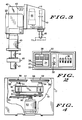
- Fig. 1 illustrates an isomeric view of a friction polisher that automatically polishes semiconductor wafers or similar workpieces.
- the polisher uses polishing arm 10 and wafer chuck 11 to move the wafer from station to station.
- These stations include load station 12, brush station 13, primary polish station 14, final polish station 15, and unload station 16.
- Stations 14 and 15 are openings in a removable cover which serves as work surface 25.
- Located below work surface 25 is a primary polish turntable and a final polish turntable. The turntables are described in greater detail hereinafter.
- the major assemblies of the polisher include cabinet 17, fluid control (behind panel 18), quill speed control (behind panel 19), control box 20, polishing arm 10, and turntable drive 61 (behind panel 21).
- Arrow 22 represents the horizontal movement of polishing arm 10. Plate 23 is discussed in the description of Fig. 3.
- the fluid control assembly located behind panel 18, is a collection of 2-way and 3-way solenoid valves, 1/4 and 3/8 inch stainless steel tubing and various assorted fittings.
- the function of the fluid control assembly is to control vacuum, hot and cold deionized (D.I.) water, high pressure D.I. water (200 P.S.I.), and primary and final slurry as directed by control box 20.
- Vacuum is used in polishing arm 10 to attach a semiconductor wafer to wafer chuck 11.
- Hot water is used at primary polish station 14 and final polish station 15 to rinse off the wafer and polishing pad.
- the polishing pads are described in greater detail hereinafter.
- Cold D.I. water is used in load station 12, primary polish station 14, final polish station 15, and unload station 16.
- a typical primary slurry is a mixture of Tizox 1300 and D.I. water and a typical final slurry is a mixture of Nalco 2355 and D.I. water. The slurrys are directed to the center of each of their respected pads.
- Quill speed control is located behind panel 19 and is used to regulate the turning speed of wafer chuck 11.
- the quill is another name for the shaft that supports wafer chuck 11.
- the two pads do not operate at the same RPM.
- the quill speed is controlled by control box 20 which regulates a D C motor.
- Leveling station 24 is used for mounting wafer chuck 11 perpendicular to quill shaft 45.
- Control box 20 is shown in greater detail in Fig. 2.
- Flowmeters 30 are used to control the amount of flow of hot D.I. water, cold D.I. water and polishing slurry for the primary and final polishing pads.
- Alarm 31 is used to advise an operator of a malfunction and lock 32 is used to prevent unauthorized personnel from changing programs.
- Display and switch assembly 33 To the left of alarm 31 is display and switch assembly 33, which is used to program a microcomputer located within control box 20. Assembly 33 has active keypad 34, function callout 35, system status lights 36 and display window 37. Function callout 35 is used as a reference index for the various functions that can be programmed through active keypad 34. System status lights 36 indicate high/low limits reached and wafer location.
- Display window 37 is a liquid crystal display (L.C.D.) which allows the function and default values to be displayed. The default values are values such as wafer diameter, polishing times, oscillation percentage, polishing arm pressures, and acceleration.
- Display window 37 continuously shows thirteen basic parameters the polisher is using.
- Display window 37, in conjunction with keypad 34 can be used to display and/or modify any of the default parameters.
- MPU microprocessor unit
- additional support electronics Located behind switch assembly 33 is a Motorola MC6809 microprocessor unit (MPU) and additional support electronics.
- MPU microprocessor unit
- the MPU is used to control and monitor all parameters throughout the polishing process.
- the computer program has "smart" reactions to various failure modes such as, loss of slurries, wafer loss, and wafers in or out of proper position in pick up or discharge pockets.
- the MPU controls wafer shape and flatness by the amount of oscillation, and acceleration factors of that oscillation during the primary polishing cycle.
- Oscillation is the stroke length of polishing arm 10, variations of which will cause the wafer flatness to go plus or minus. Acceleration is the rate of speed change at the end of each stroke.
- Behind flowmeters 30 are three motor driven pressure regulators (not shown) that are used to regulate a high, medium, and low pressure settings for polishing arm 10. The settings regulate how much force polishing arm 10 is applying against the polishing pads.
- the medium pressure setting is used to clean any dried slurry off of wafer chuck 11 which may have been formed during the polishing cycle.
- a high pressure is called for when polishing arm 10 has a wafer on wafer chuck 11 and is at primary polish station 14. This is when the majority of material is removed from the wafer or workpiece. After the wafer is deposited in unload station 16, polishing arm 10 moves to primary polishing station 14 and buffs chuck 11.
- the low pressure setting is used in the second half of the primary polishing cycle as part of a cool down cycle and is used again for the entire final polishing cycle.
- the pressure settings are monitored and adjusted by the MPU in control box 20.
- Polishing arm 10 is shown in greater detail in Fig. 3. Polishing arm 10 is supported by bearings in housing 40 and speed reducer 46. Shaft 41 is connected to speed reducer 46 and servo motor 47 which rotate shaft 41 and subsequent polishing arm 10 through 240' of horizontal rotation. Positioned behind plate cover 42 is air cylinder 43 which has a 3 1/4 inch bore and a 6 inch stroke. One end of air cylinder 42 is mounted to the upper portion of polishing arm 10. The other end of cylinder 42 is mounted to plate 23. This allows polishing arm 10 to be guided by a precision linear bearing system and move 6 inches in the vertical plane. Plate 23 is also supported by bearing housing 40 and moves in the horizontal plane but not the vertical plane. Also located inside polishing arm 10 is quill drive motor 44 and quill shaft 45.
- Quill motor 44 should be a minimum of 1/8 HP D.C. and variable speed to match turntable speeds, for example 300 RPM, and programmed by control box 20 to change speeds between primary and final polishing operations.
- the quill bearing assembly has some angular adjustments from a vertical position and is then lockable in the desired position.
- Quill shaft 45 does not run perpendicular to the turntable, in preferred embodiment quill shaft 45 is slightly less than 1 degree from perpendicular.
- the quill housing is built so that angles can be adjusted.
- One advantage to offsetting the angle of quill shaft 45 is that a smaller size quill motor 44 can be used. When quill shaft 45 and attached wafer chuck 11 make contact with a polishing pad, the pads rotational movement helps drive wafer chuck 11 in a circular motion.
- Wafer chuck 11 is attached to quill shaft 45 by neoprene hose 48.
- the end of quill shaft 45 is rounded and fits into a matching recess in wafer chuck 11.
- Hose 48 allows wafer chuck 11 a small degree of swivel movement but prevents any rotational slippage between shaft 45 and chuck 11.
- Fig. 4 illustrates a detailed view of turntable drive 61 enclosed in cabinet 17.
- main drive motor 52 is used to turn drive shafts 54 which are bolted to primary turntable 55 and final turntable 56.
- Pad plates 57 and 58 are fastened to turntables 55 and 56 by bolts 59.
- Pad plates 57, 58 are made of aluminum 22 millimeters (mm) thick and a diameter of 559 mm and 527 mm, respectively.
- Pad material for pad plate 57 is typically polyurethane foam with a porous texture such as Rhoads LP57.
- Pad material for pad plate 58 is a polyurethane impregnated fabric with a smooth texture such as Rodel 205.
- An adhesive is used to fasten the pad material to the pad plates.
- Turntables 55,56 are electroless nickel plated cast iron, and normalized for stability. Turntables 55,56, in a preferred embodiment have an outside diameter of approximately 508 mm and are flat within ⁇ 0.025 mm across the diameter.
- Turntables 55,66 are rigidly supported by bearing system 60 and can operate smoothly at approximately 300 R.P.M. continuously at up to 454.5 kilogram (kg) thrust loading plus radial loading produced by the 454.5 kg thrust load at 178 mm from center of rotation. This off-center loading will always be at the same position. It is estimated that the temperature of turntables 55,56, drive shafts 54 and bearings 60 will be about 344 K. Bearing clearances and lubrication must accommodate these temperatures continuously.
- Primary turntable 55 speed is about 300 R.P.M.
- Final turntable 56 speed is about 230 R.P.M.
- Drive motor 52 is a 7.5 HP high efficiency 3 phase 1200 R.P.M. motor with direct belt drive 50 and reduction to turntables 55 and 56. Both turntables 55,56, rotate in the same direction, counter-clock-wise (CCW).
- Final turntable 56 is operated at 77% of of table-speed of primary turntable 55.
- FIG. 5 An operational flow diagram is illustrated in Fig. 5 that represents the steps used to polish a wafer in this invention. This will provide a clearer understanding of the novelties of the invention and show how the system works.
- Block 70 represents the preparation that is needed before the polisher is turned on.
- the downward force of polishing arm 10 would cause turntable 55 to flex to some degree.
- the primary polishing pad must be shaped before it is used to polish wafers. Only the primary pad is shaped because it is here that the majority of damaged material is removed, and the highest downward pressure is applied from polishing arm 10.
- the shaping of the pad is accomplished by replacing wafer chuck 11 with a special abrasive chuck. After shaping, the center of the pad is .09 millimeters lower than the outer edge.
- This shape will produce very flat 76 mm to 150 mm wafers. Also checked or filled at this time are the primary and final slurry solutions, the settings for flowmeters 30, and the computer program in control box 20. The program is checked for proper wafer size, pressures and times.
- Block 71 represents the start of the electrical and mechanical operation of the polisher.
- the "start” button is located on control box 20.
- Block 72 represents the manual placing of a wafer into loadstation 12.
- Block 73 represents the loading or obtaining of a wafer by wafer chuck 11 from load station 12.
- Load station 12 is designed to be easily changeable for different size wafers.
- a fiber optic sensor which is used to signal polishing arm 10 that a wafer is ready for pickup.
- Wafer chuck 11, which is attached to polishing arm 10 subjects a wafer to a vacuum which is used to hold the wafer to wafer chuck 11.
- jets of water from chuck 11 scrub the backside of the wafer to remove particulates that might be present. The reason for this was that any particles trapped behind the wafer would "telegraph" a defect to the front of the wafer.
- polishing arm 10 rotates until it is over primary polish station 14.
- Air cylinder 43 causes polishing arm 10 to drop down and make contact with the pad material on pad plate 57.
- Pad plate 57 is fastened to turntable 55 which is turning at approximately 300 RPM.
- Wafer chuck 11 is also turning at 300 RPM and polishing arm 10 is oscillating from 1 to 4 inches depending on wafer size.
- primary slurry is being deposited to the center of the polishing pad. It is at this step that the majority of material is removed from the wafer.
- the second part of the primary polish cycle is the cool down cycle. Instead of slurry, cold water is deposited to the center of the polish pad.
- polishing arm 10 rotates to final polish station 15 as represented by block 76.
- a high pressure water jet 200 PSI slowly moves across the polish pad at 229 mm per minute, scrubbing off any residue. This is represented by block 75.
- Final polish turntable 56 is turning at approximately 230 RPM.
- the quill speed control (located behind panel 19) signals control box 20 which in turn signals quill motor 44 to match the speed of turntable 56. This results in wafer chuck 11 turning the same speed as turntable 56.
- the final polish cycle uses a "final slurry” and a "low” pressure setting on polishing arm 10.
- the wafer is unloaded in to station 16 which is represented by block 78.
- final polish station 15 is cleaned by a high pressure water jet as represented by block 77.
- unload station 16 is easily changeable for different size wafers.
- unload station 16 has a fiber optic sensor to detect wafers at that station. If there is a wafer in station 16 and polishing arm 10 has completed the polishing cycle with another wafer, it will hold that wafer at final polish station 15 until unload station 16 is clear. When placed on hold, station 15 is dispensing only cold water instead of slurry. This prevents the unwanted removal of additional material from the wafer.
- polishing arm 10 Once polishing arm 10 has dropped off its wafer at unload station 16, it repositions itself over primary polish station 14. Using the "medium” pressure setting, polishing arm 10 drops down on the primary polishing pad and buffs wafer chuck 11. This is represented by block 79. The purpose of the buffing is to remove any dried slurry that might be remaining on wafer chuck 11.
- polishing arm 10 moves to brush station 13, which is represented by block 80.
- brush station 13 the vacuum channels that are in wafer chuck 11 are cleaned out by simultaneously rotating chuck 11 against the brushes and blowing water out the opening in the chuck.
- polishing arm 10 If polishing arm 10 detects another wafer in load station 12, it will then repeat the cycle. This is represented by block 81.
- the resulting device is a computer controlled friction polisher that can automatically do both the primary polish and the final polish and obtain ultra-flat wafers with less breakage and defects. This is accomplished in part with the use of cleaning devices such as water scrubbing the back of the wafer, water jets on the polishing pads, buffing the wafer chuck and brush scrubbing the wafer chuck.
- cleaning devices such as water scrubbing the back of the wafer, water jets on the polishing pads, buffing the wafer chuck and brush scrubbing the wafer chuck.
- operator error is reduced due to the use of the MPU which automatically sets pressures, oscillation, acceleration, times, etc., when the operator enters the size of the wafer to be polished.
Landscapes
- Engineering & Computer Science (AREA)
- Computer Hardware Design (AREA)
- Physics & Mathematics (AREA)
- Condensed Matter Physics & Semiconductors (AREA)
- General Physics & Mathematics (AREA)
- Manufacturing & Machinery (AREA)
- Mechanical Engineering (AREA)
- Microelectronics & Electronic Packaging (AREA)
- Power Engineering (AREA)
- Finish Polishing, Edge Sharpening, And Grinding By Specific Grinding Devices (AREA)
- Mechanical Treatment Of Semiconductor (AREA)
- Cleaning Or Drying Semiconductors (AREA)
- Constituent Portions Of Griding Lathes, Driving, Sensing And Control (AREA)
Applications Claiming Priority (2)
| Application Number | Priority Date | Filing Date | Title |
|---|---|---|---|
| US06/779,339 US4680893A (en) | 1985-09-23 | 1985-09-23 | Apparatus for polishing semiconductor wafers |
| US779339 | 1985-09-23 |
Publications (3)
| Publication Number | Publication Date |
|---|---|
| EP0216054A2 true EP0216054A2 (de) | 1987-04-01 |
| EP0216054A3 EP0216054A3 (en) | 1989-03-01 |
| EP0216054B1 EP0216054B1 (de) | 1992-05-20 |
Family
ID=25116105
Family Applications (1)
| Application Number | Title | Priority Date | Filing Date |
|---|---|---|---|
| EP86109817A Expired - Lifetime EP0216054B1 (de) | 1985-09-23 | 1986-07-17 | Vorrichtung zum Polieren von Halbleiterscheiben |
Country Status (5)
| Country | Link |
|---|---|
| US (1) | US4680893A (de) |
| EP (1) | EP0216054B1 (de) |
| JP (1) | JP2572577B2 (de) |
| KR (1) | KR920009984B1 (de) |
| DE (1) | DE3685386D1 (de) |
Cited By (1)
| Publication number | Priority date | Publication date | Assignee | Title |
|---|---|---|---|---|
| EP0584905A1 (de) * | 1992-07-31 | 1994-03-02 | Shin-Etsu Handotai Company Limited | Vorrichtung zum Polieren von Fasen auf Halbleiterscheiben |
Families Citing this family (112)
| Publication number | Priority date | Publication date | Assignee | Title |
|---|---|---|---|---|
| US4839993A (en) * | 1986-01-28 | 1989-06-20 | Fujisu Limited | Polishing machine for ferrule of optical fiber connector |
| US4837979A (en) * | 1987-03-17 | 1989-06-13 | Sintobrator, Ltd. | Polishing device |
| JPH02253903A (ja) * | 1989-03-29 | 1990-10-12 | Takahiro Imahashi | 自動ファセティングマシン |
| JPH089139B2 (ja) * | 1990-02-02 | 1996-01-31 | 不二越機械工業株式会社 | ポリシング装置およびポリシング方法 |
| USRE36890E (en) * | 1990-07-31 | 2000-10-03 | Motorola, Inc. | Gradient chuck method for wafer bonding employing a convex pressure |
| US5320706A (en) * | 1991-10-15 | 1994-06-14 | Texas Instruments Incorporated | Removing slurry residue from semiconductor wafer planarization |
| JPH0615565A (ja) * | 1991-12-18 | 1994-01-25 | Shin Etsu Handotai Co Ltd | ウエーハ自動ラッピング装置 |
| JP2789153B2 (ja) * | 1992-01-27 | 1998-08-20 | マイクロン テクノロジー インコーポレイテッド | マイクロスクラッチのない平滑面を形成するための半導体ウェハの化学機械的平坦化方法 |
| US5514245A (en) * | 1992-01-27 | 1996-05-07 | Micron Technology, Inc. | Method for chemical planarization (CMP) of a semiconductor wafer to provide a planar surface free of microscratches |
| US5245794A (en) * | 1992-04-09 | 1993-09-21 | Advanced Micro Devices, Inc. | Audio end point detector for chemical-mechanical polishing and method therefor |
| US5329732A (en) | 1992-06-15 | 1994-07-19 | Speedfam Corporation | Wafer polishing method and apparatus |
| US5498199A (en) * | 1992-06-15 | 1996-03-12 | Speedfam Corporation | Wafer polishing method and apparatus |
| JP2655975B2 (ja) * | 1992-09-18 | 1997-09-24 | 三菱マテリアル株式会社 | ウェーハ研磨装置 |
| US5487697A (en) * | 1993-02-09 | 1996-01-30 | Rodel, Inc. | Polishing apparatus and method using a rotary work holder travelling down a rail for polishing a workpiece with linear pads |
| US5443416A (en) * | 1993-09-09 | 1995-08-22 | Cybeq Systems Incorporated | Rotary union for coupling fluids in a wafer polishing apparatus |
| US5885138A (en) | 1993-09-21 | 1999-03-23 | Ebara Corporation | Method and apparatus for dry-in, dry-out polishing and washing of a semiconductor device |
| JP2513426B2 (ja) * | 1993-09-20 | 1996-07-03 | 日本電気株式会社 | ウェ―ハ研磨装置 |
| KR100390293B1 (ko) * | 1993-09-21 | 2003-09-02 | 가부시끼가이샤 도시바 | 폴리싱장치 |
| US5531861A (en) * | 1993-09-29 | 1996-07-02 | Motorola, Inc. | Chemical-mechanical-polishing pad cleaning process for use during the fabrication of semiconductor devices |
| JP3326642B2 (ja) * | 1993-11-09 | 2002-09-24 | ソニー株式会社 | 基板の研磨後処理方法およびこれに用いる研磨装置 |
| US5938504A (en) * | 1993-11-16 | 1999-08-17 | Applied Materials, Inc. | Substrate polishing apparatus |
| US5653623A (en) * | 1993-12-14 | 1997-08-05 | Ebara Corporation | Polishing apparatus with improved exhaust |
| US5643053A (en) * | 1993-12-27 | 1997-07-01 | Applied Materials, Inc. | Chemical mechanical polishing apparatus with improved polishing control |
| US5582534A (en) * | 1993-12-27 | 1996-12-10 | Applied Materials, Inc. | Orbital chemical mechanical polishing apparatus and method |
| US5650039A (en) * | 1994-03-02 | 1997-07-22 | Applied Materials, Inc. | Chemical mechanical polishing apparatus with improved slurry distribution |
| US5795495A (en) * | 1994-04-25 | 1998-08-18 | Micron Technology, Inc. | Method of chemical mechanical polishing for dielectric layers |
| US5733175A (en) * | 1994-04-25 | 1998-03-31 | Leach; Michael A. | Polishing a workpiece using equal velocity at all points overlapping a polisher |
| US5449314A (en) * | 1994-04-25 | 1995-09-12 | Micron Technology, Inc. | Method of chimical mechanical polishing for dielectric layers |
| US5679060A (en) * | 1994-07-14 | 1997-10-21 | Silicon Technology Corporation | Wafer grinding machine |
| US5534106A (en) * | 1994-07-26 | 1996-07-09 | Kabushiki Kaisha Toshiba | Apparatus for processing semiconductor wafers |
| US5607341A (en) * | 1994-08-08 | 1997-03-04 | Leach; Michael A. | Method and structure for polishing a wafer during manufacture of integrated circuits |
| DE19544328B4 (de) * | 1994-11-29 | 2014-03-20 | Ebara Corp. | Poliervorrichtung |
| US5558111A (en) * | 1995-02-02 | 1996-09-24 | International Business Machines Corporation | Apparatus and method for carrier backing film reconditioning |
| US5769696A (en) * | 1995-02-10 | 1998-06-23 | Advanced Micro Devices, Inc. | Chemical-mechanical polishing of thin materials using non-baked carrier film |
| JP2647050B2 (ja) * | 1995-03-31 | 1997-08-27 | 日本電気株式会社 | ウェハ研磨装置 |
| US5593343A (en) * | 1995-04-03 | 1997-01-14 | Bauer; Jason | Apparatus for reconditioning digital recording discs |
| US5954566A (en) * | 1995-04-03 | 1999-09-21 | Bauer; Jason | Method and apparatus for reconditioning digital recording discs |
| JP3690837B2 (ja) * | 1995-05-02 | 2005-08-31 | 株式会社荏原製作所 | ポリッシング装置及び方法 |
| US5578529A (en) * | 1995-06-02 | 1996-11-26 | Motorola Inc. | Method for using rinse spray bar in chemical mechanical polishing |
| US5816891A (en) * | 1995-06-06 | 1998-10-06 | Advanced Micro Devices, Inc. | Performing chemical mechanical polishing of oxides and metals using sequential removal on multiple polish platens to increase equipment throughput |
| US6110820A (en) * | 1995-06-07 | 2000-08-29 | Micron Technology, Inc. | Low scratch density chemical mechanical planarization process |
| JP3678468B2 (ja) * | 1995-07-18 | 2005-08-03 | 株式会社荏原製作所 | ポリッシング装置 |
| JP2850803B2 (ja) * | 1995-08-01 | 1999-01-27 | 信越半導体株式会社 | ウエーハ研磨方法 |
| KR100487590B1 (ko) * | 1995-08-21 | 2005-08-04 | 가부시키가이샤 에바라 세이사꾸쇼 | 폴리싱장치 |
| US5685766A (en) * | 1995-11-30 | 1997-11-11 | Speedfam Corporation | Polishing control method |
| US6050884A (en) * | 1996-02-28 | 2000-04-18 | Ebara Corporation | Polishing apparatus |
| US5800254A (en) * | 1996-04-01 | 1998-09-01 | Buehler Ltd. | Automatic apparatus for grinding and polishing samples |
| JP3696690B2 (ja) * | 1996-04-23 | 2005-09-21 | 不二越機械工業株式会社 | ウェーハの研磨装置システム |
| US6012966A (en) * | 1996-05-10 | 2000-01-11 | Canon Kabushiki Kaisha | Precision polishing apparatus with detecting means |
| JP2000315665A (ja) * | 1999-04-29 | 2000-11-14 | Ebara Corp | 研磨方法及び装置 |
| US6413156B1 (en) * | 1996-05-16 | 2002-07-02 | Ebara Corporation | Method and apparatus for polishing workpiece |
| EP0807492B1 (de) * | 1996-05-16 | 2003-03-19 | Ebara Corporation | Verfahren und Vorrichtung zum Polieren von Werkstücken |
| KR100241537B1 (ko) * | 1996-06-21 | 2000-02-01 | 김영환 | 반도체 소자의 층간 절연막 평탄화 방법 |
| US6537137B2 (en) | 1996-08-16 | 2003-03-25 | Rodel Holdings, Inc | Methods for chemical-mechanical polishing of semiconductor wafers |
| US5932486A (en) * | 1996-08-16 | 1999-08-03 | Rodel, Inc. | Apparatus and methods for recirculating chemical-mechanical polishing of semiconductor wafers |
| US6245679B1 (en) | 1996-08-16 | 2001-06-12 | Rodel Holdings, Inc | Apparatus and methods for chemical-mechanical polishing of semiconductor wafers |
| US6210525B1 (en) | 1996-08-16 | 2001-04-03 | Rodel Holdings, Inc. | Apparatus and methods for chemical-mechanical polishing of semiconductor wafers |
| US6200201B1 (en) * | 1996-08-29 | 2001-03-13 | Lam Research Corporation | Cleaning/buffer apparatus for use in a wafer processing device |
| US5702292A (en) * | 1996-10-31 | 1997-12-30 | Micron Technology, Inc. | Apparatus and method for loading and unloading substrates to a chemical-mechanical planarization machine |
| US5716258A (en) * | 1996-11-26 | 1998-02-10 | Metcalf; Robert L. | Semiconductor wafer polishing machine and method |
| US6379221B1 (en) | 1996-12-31 | 2002-04-30 | Applied Materials, Inc. | Method and apparatus for automatically changing a polishing pad in a chemical mechanical polishing system |
| US6012970A (en) * | 1997-01-15 | 2000-01-11 | Motorola, Inc. | Process for forming a semiconductor device |
| TW426556B (en) * | 1997-01-24 | 2001-03-21 | United Microelectronics Corp | Method of cleaning slurry remnants left on a chemical-mechanical polish machine |
| JP3705670B2 (ja) * | 1997-02-19 | 2005-10-12 | 株式会社荏原製作所 | ポリッシング装置及び方法 |
| US6120352A (en) * | 1997-03-06 | 2000-09-19 | Keltech Engineering | Lapping apparatus and lapping method using abrasive sheets |
| US6048254A (en) * | 1997-03-06 | 2000-04-11 | Keltech Engineering | Lapping apparatus and process with annular abrasive area |
| US5967882A (en) * | 1997-03-06 | 1999-10-19 | Keltech Engineering | Lapping apparatus and process with two opposed lapping platens |
| US6149506A (en) * | 1998-10-07 | 2000-11-21 | Keltech Engineering | Lapping apparatus and method for high speed lapping with a rotatable abrasive platen |
| JPH10329015A (ja) * | 1997-03-24 | 1998-12-15 | Canon Inc | 研磨装置および研磨方法 |
| US6244946B1 (en) | 1997-04-08 | 2001-06-12 | Lam Research Corporation | Polishing head with removable subcarrier |
| US6425812B1 (en) | 1997-04-08 | 2002-07-30 | Lam Research Corporation | Polishing head for chemical mechanical polishing using linear planarization technology |
| US6139406A (en) | 1997-06-24 | 2000-10-31 | Applied Materials, Inc. | Combined slurry dispenser and rinse arm and method of operation |
| JPH1187286A (ja) | 1997-09-05 | 1999-03-30 | Lsi Logic Corp | 半導体ウエハの二段階式化学的機械的研磨方法及び装置 |
| US6213853B1 (en) | 1997-09-10 | 2001-04-10 | Speedfam-Ipec Corporation | Integral machine for polishing, cleaning, rinsing and drying workpieces |
| US6190237B1 (en) | 1997-11-06 | 2001-02-20 | International Business Machines Corporation | pH-buffered slurry and use thereof for polishing |
| US6336845B1 (en) | 1997-11-12 | 2002-01-08 | Lam Research Corporation | Method and apparatus for polishing semiconductor wafers |
| US5972162A (en) * | 1998-01-06 | 1999-10-26 | Speedfam Corporation | Wafer polishing with improved end point detection |
| US6102777A (en) * | 1998-03-06 | 2000-08-15 | Keltech Engineering | Lapping apparatus and method for high speed lapping with a rotatable abrasive platen |
| JP3615931B2 (ja) * | 1998-03-26 | 2005-02-02 | 株式会社荏原製作所 | ポリッシング装置および該ポリッシング装置におけるコンディショニング方法 |
| FR2776552B1 (fr) | 1998-03-31 | 2000-06-16 | Procedes & Equipement Pour Les | Machine modulaire de polissage et de planarisation de substrats |
| US6102782A (en) * | 1998-04-06 | 2000-08-15 | Micron Technology, Inc. | System and apparatus for distributing flush fluid to processing equipment |
| US6257966B1 (en) * | 1998-04-27 | 2001-07-10 | Tokyo Seimitsu Co., Ltd. | Wafer surface machining apparatus |
| US6391779B1 (en) | 1998-08-11 | 2002-05-21 | Micron Technology, Inc. | Planarization process |
| US6220941B1 (en) * | 1998-10-01 | 2001-04-24 | Applied Materials, Inc. | Method of post CMP defect stability improvement |
| JP2000133623A (ja) * | 1998-10-28 | 2000-05-12 | Toshiba Corp | 平坦化方法及び平坦化装置 |
| US6319098B1 (en) | 1998-11-13 | 2001-11-20 | Applied Materials, Inc. | Method of post CMP defect stability improvement |
| US6165052A (en) * | 1998-11-16 | 2000-12-26 | Taiwan Semiconductor Manufacturing Company | Method and apparatus for chemical/mechanical planarization (CMP) of a semiconductor substrate having shallow trench isolation |
| US6521536B1 (en) | 1999-01-11 | 2003-02-18 | Micron Technology, Inc. | Planarization process |
| US6368189B1 (en) | 1999-03-03 | 2002-04-09 | Mitsubishi Materials Corporation | Apparatus and method for chemical-mechanical polishing (CMP) head having direct pneumatic wafer polishing pressure |
| US6231428B1 (en) | 1999-03-03 | 2001-05-15 | Mitsubishi Materials Corporation | Chemical mechanical polishing head assembly having floating wafer carrier and retaining ring |
| US6358128B1 (en) | 1999-03-05 | 2002-03-19 | Ebara Corporation | Polishing apparatus |
| US6354922B1 (en) | 1999-08-20 | 2002-03-12 | Ebara Corporation | Polishing apparatus |
| US6352595B1 (en) * | 1999-05-28 | 2002-03-05 | Lam Research Corporation | Method and system for cleaning a chemical mechanical polishing pad |
| US6261159B1 (en) * | 1999-07-06 | 2001-07-17 | Kevin Krieg | Apparatus and method for the restoration of optical storage media |
| US6083082A (en) * | 1999-08-30 | 2000-07-04 | Lam Research Corporation | Spindle assembly for force controlled polishing |
| US6431959B1 (en) | 1999-12-20 | 2002-08-13 | Lam Research Corporation | System and method of defect optimization for chemical mechanical planarization of polysilicon |
| US6669538B2 (en) | 2000-02-24 | 2003-12-30 | Applied Materials Inc | Pad cleaning for a CMP system |
| US6666756B1 (en) | 2000-03-31 | 2003-12-23 | Lam Research Corporation | Wafer carrier head assembly |
| JP2001326201A (ja) * | 2000-05-16 | 2001-11-22 | Ebara Corp | ポリッシング装置 |
| US6659116B1 (en) | 2000-06-26 | 2003-12-09 | Lam Research Corporation | System for wafer carrier in-process clean and rinse |
| US6505636B1 (en) | 2000-06-26 | 2003-01-14 | Lam Research Corporation | Apparatus for wafer carrier in-process clean and rinse |
| US6409580B1 (en) * | 2001-03-26 | 2002-06-25 | Speedfam-Ipec Corporation | Rigid polishing pad conditioner for chemical mechanical polishing tool |
| US6599174B1 (en) * | 2001-04-27 | 2003-07-29 | Advanced Micro Devices, Inc. | Eliminating dishing non-uniformity of a process layer |
| JP3530158B2 (ja) * | 2001-08-21 | 2004-05-24 | 沖電気工業株式会社 | 半導体装置及びその製造方法 |
| US6585567B1 (en) | 2001-08-31 | 2003-07-01 | Koninklijke Philips Electronics N.V. | Short CMP polish method |
| JP2003211355A (ja) * | 2002-01-15 | 2003-07-29 | Ebara Corp | ポリッシング装置及びドレッシング方法 |
| US20060180486A1 (en) * | 2003-04-21 | 2006-08-17 | Bennett David W | Modular panel and storage system for flat items such as media discs and holders therefor |
| US8574028B2 (en) * | 2008-06-20 | 2013-11-05 | Illinois Tool Works Inc. | Grinder/polisher |
| JP6209088B2 (ja) * | 2013-01-25 | 2017-10-04 | 株式会社荏原製作所 | 研磨方法および装置 |
| KR20160125585A (ko) * | 2015-04-21 | 2016-11-01 | 삼성전자주식회사 | 기판 처리 장치 및 기판 처리 방법 |
| US20210299815A1 (en) * | 2020-03-31 | 2021-09-30 | Illinois Tool Works Inc. | Grinding/polishing devices with recall |
| TWI766728B (zh) * | 2021-06-16 | 2022-06-01 | 均豪精密工業股份有限公司 | 研磨裝置 |
Citations (5)
| Publication number | Priority date | Publication date | Assignee | Title |
|---|---|---|---|---|
| DE1914082A1 (de) * | 1968-03-22 | 1969-10-02 | Ibm | Verfahren und Vorrichtung zum Polieren von Werkstueckoberflaechen |
| FR2232085A1 (de) * | 1973-05-29 | 1974-12-27 | Rca Corp | |
| US3977130A (en) * | 1975-05-12 | 1976-08-31 | Semimetals, Inc. | Removal-compensating polishing apparatus |
| US4141180A (en) * | 1977-09-21 | 1979-02-27 | Kayex Corporation | Polishing apparatus |
| GB2072550A (en) * | 1980-03-27 | 1981-10-07 | Monsanto Co | Method and apparatus for improving flatness of polished wafers |
Family Cites Families (4)
| Publication number | Priority date | Publication date | Assignee | Title |
|---|---|---|---|---|
| GB1377837A (en) * | 1972-10-18 | 1974-12-18 | Dolgov V M | Machine for simultaneous grinding of a plurality of semiconduct or blanks |
| DE2451549A1 (de) * | 1974-10-30 | 1976-08-12 | Mueller Georg Kugellager | Belade- und entladevorrichtung fuer plattenfoermige halbleitermaterialien |
| US4239567A (en) * | 1978-10-16 | 1980-12-16 | Western Electric Company, Inc. | Removably holding planar articles for polishing operations |
| JPS58192750A (ja) * | 1982-05-03 | 1983-11-10 | Toyoda Mach Works Ltd | 研削盤 |
-
1985
- 1985-09-23 US US06/779,339 patent/US4680893A/en not_active Expired - Lifetime
-
1986
- 1986-07-17 DE DE8686109817T patent/DE3685386D1/de not_active Expired - Lifetime
- 1986-07-17 EP EP86109817A patent/EP0216054B1/de not_active Expired - Lifetime
- 1986-09-19 JP JP61219898A patent/JP2572577B2/ja not_active Expired - Lifetime
- 1986-09-22 KR KR1019860007902A patent/KR920009984B1/ko not_active IP Right Cessation
Patent Citations (5)
| Publication number | Priority date | Publication date | Assignee | Title |
|---|---|---|---|---|
| DE1914082A1 (de) * | 1968-03-22 | 1969-10-02 | Ibm | Verfahren und Vorrichtung zum Polieren von Werkstueckoberflaechen |
| FR2232085A1 (de) * | 1973-05-29 | 1974-12-27 | Rca Corp | |
| US3977130A (en) * | 1975-05-12 | 1976-08-31 | Semimetals, Inc. | Removal-compensating polishing apparatus |
| US4141180A (en) * | 1977-09-21 | 1979-02-27 | Kayex Corporation | Polishing apparatus |
| GB2072550A (en) * | 1980-03-27 | 1981-10-07 | Monsanto Co | Method and apparatus for improving flatness of polished wafers |
Cited By (3)
| Publication number | Priority date | Publication date | Assignee | Title |
|---|---|---|---|---|
| EP0584905A1 (de) * | 1992-07-31 | 1994-03-02 | Shin-Etsu Handotai Company Limited | Vorrichtung zum Polieren von Fasen auf Halbleiterscheiben |
| US5547415A (en) * | 1992-07-31 | 1996-08-20 | Shin-Etsu Handotai Co., Ltd. | Method and apparatus for wafer chamfer polishing |
| US6234879B1 (en) | 1992-07-31 | 2001-05-22 | Shin-Etsu Handotai Co., Ltd. | Method and apparatus for wafer chamfer polishing |
Also Published As
| Publication number | Publication date |
|---|---|
| EP0216054B1 (de) | 1992-05-20 |
| KR920009984B1 (ko) | 1992-11-09 |
| EP0216054A3 (en) | 1989-03-01 |
| KR870003555A (ko) | 1987-04-18 |
| DE3685386D1 (de) | 1992-06-25 |
| JPS6268273A (ja) | 1987-03-28 |
| US4680893A (en) | 1987-07-21 |
| JP2572577B2 (ja) | 1997-01-16 |
Similar Documents
| Publication | Publication Date | Title |
|---|---|---|
| US4680893A (en) | Apparatus for polishing semiconductor wafers | |
| KR100780588B1 (ko) | 반도체 기판의 평탄화 장치 및 방법 | |
| KR100315722B1 (ko) | 기판표면을평탄화하기위한연마기 | |
| US6106369A (en) | Polishing system | |
| US6093087A (en) | Wafer processing machine and a processing method thereby | |
| US6241585B1 (en) | Apparatus and method for chemical mechanical polishing | |
| US20020013124A1 (en) | Polishing apparatus | |
| US20020160691A1 (en) | Planarization apparatus and method | |
| US6409580B1 (en) | Rigid polishing pad conditioner for chemical mechanical polishing tool | |
| US20030153250A1 (en) | Subaperture chemical mechanical planarization with polishing pad conditioning | |
| KR20020020692A (ko) | 웨이퍼 연마 패드의 조절 방법 | |
| US6783440B2 (en) | Polishing apparatus | |
| US6607427B2 (en) | Dressing apparatus and polishing apparatus | |
| JPH0761601B2 (ja) | ウエハの鏡面加工方法 | |
| KR101962090B1 (ko) | 웨이퍼 폴리싱 장치 및 그 방법 | |
| JP4808278B2 (ja) | 平面加工装置及び方法 | |
| JP2006272546A (ja) | 研磨装置及び研磨方法 | |
| JP2006222467A (ja) | 平面加工装置 | |
| JP2651479B2 (ja) | ウエハの鏡面加工装置 | |
| WO2001058644A1 (en) | Method and apparatus for controlling a pad conditioning process of a chemical-mechanical polishing apparatus | |
| JP2001148361A (ja) | 研磨装置、研磨パッド部材交換装置および方法 | |
| JP4205263B2 (ja) | 自動ラップ装置およびそれを用いる基板の研磨方法 | |
| KR20010029637A (ko) | 연마패드의 교환장치 및 연마패드의 교환방법 | |
| JPH06246624A (ja) | 両面研磨装置 | |
| WO2001082353A1 (fr) | Dispositif et procede de polissage du chanfrein peripherique d'une tranche de silicium |
Legal Events
| Date | Code | Title | Description |
|---|---|---|---|
| PUAI | Public reference made under article 153(3) epc to a published international application that has entered the european phase |
Free format text: ORIGINAL CODE: 0009012 |
|
| AK | Designated contracting states |
Kind code of ref document: A2 Designated state(s): DE FR IT |
|
| PUAL | Search report despatched |
Free format text: ORIGINAL CODE: 0009013 |
|
| AK | Designated contracting states |
Kind code of ref document: A3 Designated state(s): DE FR IT |
|
| 17P | Request for examination filed |
Effective date: 19890817 |
|
| 17Q | First examination report despatched |
Effective date: 19901016 |
|
| GRAA | (expected) grant |
Free format text: ORIGINAL CODE: 0009210 |
|
| ITF | It: translation for a ep patent filed |
Owner name: BARZANO' E ZANARDO ROMA S.P.A. |
|
| AK | Designated contracting states |
Kind code of ref document: B1 Designated state(s): DE FR IT |
|
| REF | Corresponds to: |
Ref document number: 3685386 Country of ref document: DE Date of ref document: 19920625 |
|
| ET | Fr: translation filed | ||
| PLBE | No opposition filed within time limit |
Free format text: ORIGINAL CODE: 0009261 |
|
| STAA | Information on the status of an ep patent application or granted ep patent |
Free format text: STATUS: NO OPPOSITION FILED WITHIN TIME LIMIT |
|
| 26N | No opposition filed | ||
| PGFP | Annual fee paid to national office [announced via postgrant information from national office to epo] |
Ref country code: FR Payment date: 19980707 Year of fee payment: 13 |
|
| PG25 | Lapsed in a contracting state [announced via postgrant information from national office to epo] |
Ref country code: FR Free format text: THE PATENT HAS BEEN ANNULLED BY A DECISION OF A NATIONAL AUTHORITY Effective date: 19990731 |
|
| REG | Reference to a national code |
Ref country code: FR Ref legal event code: ST |
|
| PG25 | Lapsed in a contracting state [announced via postgrant information from national office to epo] |
Ref country code: IT Free format text: LAPSE BECAUSE OF NON-PAYMENT OF DUE FEES;WARNING: LAPSES OF ITALIAN PATENTS WITH EFFECTIVE DATE BEFORE 2007 MAY HAVE OCCURRED AT ANY TIME BEFORE 2007. THE CORRECT EFFECTIVE DATE MAY BE DIFFERENT FROM THE ONE RECORDED. Effective date: 20050717 |
|
| PGFP | Annual fee paid to national office [announced via postgrant information from national office to epo] |
Ref country code: DE Payment date: 20050729 Year of fee payment: 20 |