EP0198170A2 - Circuit moniteur - Google Patents
Circuit moniteur Download PDFInfo
- Publication number
- EP0198170A2 EP0198170A2 EP86101917A EP86101917A EP0198170A2 EP 0198170 A2 EP0198170 A2 EP 0198170A2 EP 86101917 A EP86101917 A EP 86101917A EP 86101917 A EP86101917 A EP 86101917A EP 0198170 A2 EP0198170 A2 EP 0198170A2
- Authority
- EP
- European Patent Office
- Prior art keywords
- data
- input
- output
- circuit
- bus
- Prior art date
- Legal status (The legal status is an assumption and is not a legal conclusion. Google has not performed a legal analysis and makes no representation as to the accuracy of the status listed.)
- Granted
Links
Images


Classifications
-
- G—PHYSICS
- G06—COMPUTING; CALCULATING OR COUNTING
- G06F—ELECTRIC DIGITAL DATA PROCESSING
- G06F11/00—Error detection; Error correction; Monitoring
- G06F11/07—Responding to the occurrence of a fault, e.g. fault tolerance
- G06F11/0703—Error or fault processing not based on redundancy, i.e. by taking additional measures to deal with the error or fault not making use of redundancy in operation, in hardware, or in data representation
- G06F11/0751—Error or fault detection not based on redundancy
- G06F11/0763—Error or fault detection not based on redundancy by bit configuration check, e.g. of formats or tags
-
- G—PHYSICS
- G05—CONTROLLING; REGULATING
- G05B—CONTROL OR REGULATING SYSTEMS IN GENERAL; FUNCTIONAL ELEMENTS OF SUCH SYSTEMS; MONITORING OR TESTING ARRANGEMENTS FOR SUCH SYSTEMS OR ELEMENTS
- G05B19/00—Programme-control systems
- G05B19/02—Programme-control systems electric
- G05B19/04—Programme control other than numerical control, i.e. in sequence controllers or logic controllers
- G05B19/05—Programmable logic controllers, e.g. simulating logic interconnections of signals according to ladder diagrams or function charts
- G05B19/058—Safety, monitoring
-
- G—PHYSICS
- G05—CONTROLLING; REGULATING
- G05B—CONTROL OR REGULATING SYSTEMS IN GENERAL; FUNCTIONAL ELEMENTS OF SUCH SYSTEMS; MONITORING OR TESTING ARRANGEMENTS FOR SUCH SYSTEMS OR ELEMENTS
- G05B2219/00—Program-control systems
- G05B2219/10—Plc systems
- G05B2219/11—Plc I-O input output
- G05B2219/1194—Send dummy, check data to I-O to check correct I-O connection
-
- G—PHYSICS
- G05—CONTROLLING; REGULATING
- G05B—CONTROL OR REGULATING SYSTEMS IN GENERAL; FUNCTIONAL ELEMENTS OF SUCH SYSTEMS; MONITORING OR TESTING ARRANGEMENTS FOR SUCH SYSTEMS OR ELEMENTS
- G05B2219/00—Program-control systems
- G05B2219/10—Plc systems
- G05B2219/11—Plc I-O input output
- G05B2219/1199—Inserting or taking out of boards during power on, hot plug in
-
- G—PHYSICS
- G06—COMPUTING; CALCULATING OR COUNTING
- G06F—ELECTRIC DIGITAL DATA PROCESSING
- G06F11/00—Error detection; Error correction; Monitoring
- G06F11/22—Detection or location of defective computer hardware by testing during standby operation or during idle time, e.g. start-up testing
- G06F11/26—Functional testing
- G06F11/273—Tester hardware, i.e. output processing circuits
- G06F11/277—Tester hardware, i.e. output processing circuits with comparison between actual response and known fault-free response
Definitions
- This invention relates to a monitor circuit, more particularly to a monitor circuit for use with an input/output bus of a data processing device such as a programmable controller.
- a programmable controller (hereinafter referred to as PC) normally has a bus gate circuit connected between a data bus of a CPU and an input/output bus connected to input/output units.
- PC programmable controller
- the input/output units comprises a plurality of input units and output units.
- Such signal sources as limit switches, photo-electric switches, and proximity switches are connected to the input units and such output devices as motors, electro-magnetic valves, and pomps are connected to the output units.
- the input/output unit plays a role of an interface connecting the PC to the equipment to be controlled and cnstitutes the portion which is subject to the worst electric environment in each component of the PC. Accordingly, it is of very importance to design the PC in such a manner that neither the input/output unit nor input/output bus are protected against malfunction caused by external noises.
- the input/output data may be adversely affected, thus causing malfunction to the PC.
- a monitor circuit comprising means for transmitting a dummy data through a buffer circuit to an input/out bus connected to an inputioutput unit during the time when a bus-gate circuit connected between the input/output bus and a data bus is closed, and means for judging whether or not the dummy data is correctly transmitted to the input/output bus under the operation of the transferring means.
- FIG. 1 there is shown a whole construction of a PC.
- a CPU 10 is constituted by MOTOROLA 6809 to which a system memory 12 for storing a system program, user program memory 14, input/output (UO) memory 18, and program console 20 are connected respectively.
- Each I/O unit 16 NO. 0 through N plays a role of either input unit or output unit.
- a bus gate circuit 22 is connected between a data bus DBN connected to CPU 10 and I/O bus IODN connected to each I/O unit.
- a monitor circuit 24 is connected between the output and input of bus gate circuit 22.
- DBN, IODN, and bus gate circuit 22 are shown to handle only one bit for the purpose of the simplification of description, actually they will be provided corresponding to the number of the output terminal of each I/O unit.
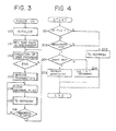
- a step 100 each part of the PC is initialized.
- the next step is also initializing step which is described hereinafter.
- a step 102 a user program stored in
- memory 14 is executed down to its end command based on the data stored in I/0 memory 18 and rewrite the output data of I/O memory 18 according to the results of its execution.
- the next step 103 is provided to display processing conditions at program console 20 or to receive various instructions therefrom. Then. an abnormal flag FLG of monitor circuit 24 is cleared by a signal FGC (step 104).
- the next step 105 is provided for I/O refresh processing. That is, the output data of I/O memory 18 rewriten by the execution of the user program are transferred to the corresponding output unit 16 and the latest input data of the input unit 16 are taken into the I/0 memory 18 and stored therein.
- step 106 After completing I/O refresh processing, it is inquired if the abnormal flag FLG is set or cleared - (step 106). If the FLG remains cleared, it implies that the I/O refresh processing has been correctly completed. In this case, a sequence returns to the step 102 which is, as previously described, an execution routine of the user program. If the FLG is set, it implies that the disturbance has been caused to the 1/0 bus IODn during the I/O refresh processing and that the transferred data has been probably changed. In this case, a sequence flows to the step 104 to 105, and the I/O refresh processing will be retried.
- monitor circuit 24 comprises data memory 26 storing a given bit pattern of dummy data, buffer circuit 28 connected between the output of memory 26 and IODn, multiplexer 30 adapted to select either dummy data from memory 26 or the data on CPU data bus DBn, coincidence circuit 32 comparing the data on IODn with the selected data by multiplexer 30, flag circuit 34 establishing the abnormal flag FLG responsive to the non-coincidence output from coincidence circuit 32, and timing generator 36 adapted to generate timing signals G1,G2,G3, and G4 based on the system clocks EE and EQ, and control signals R/W and DLD transmitted from CPU 10.
- the step 101 shown in Fig. 3 is a routine for setting dummy data (test data) into the data memory 26.
- Fig. 5 there is shown a time chart illustrating the operation of CPU 10 accessing to I/0 units 16 and the opration of monitor circuit 24. Firstly described is an Access Mode (Write Mode) with respect to output units 16.
- the non-coincidence output of coincidence circuit 32 is read into flag circuit 34 with the rise of signal IOEN.
- Access Mode (Read Mode) with respect to input units 16.
- CPU 10 will select by channel select signals IOCHi the input unit 16 to be accessed, and lower the levels of signals IOEN and ING in the latter-half portion of a CPU machine cycle.
- the input data of the selected input unit 16 is output to IODn, taken into DBn through bus gate circuit 22 and writen into I/0 memory 18.
- multiplexer 30 of monitor circuit 24 is switched to select the dummy data from data memory 26 and buffer circuit 28 is opened immediately before the levels of signals IOEN and ING are lowered. That is, the dummy data of data memory 26 is transmitted through buffer circuit 28 onto IODn immediately before the input gate of bus gate circuit 22 is opened to allow the Read Mode Access. And then, the data on IODn is compared with the data of data memory 26 in coincidence circuit 32. As previously described, unless the disturbance is caused to IODn, the both data are expected to coincide with each other, while in case such disturbance is caused there is a possibility of non-coincidence between the both data. The output of non-coincidence is read into flag circuit 34 in synchronization with the rise of clock EE.
- the monitoring operation of IODn by the use of dummy data is also performed according to the same timing mentioned above when CPU 10 accesses memories 12,14 and 18 and program console 20.
- IO Dn is monitored not only by the use of dummy data when bus gate circuit 22 is closed, but by the use of the output data transmitted from CPU through DBn by opening gate circuit 22. Accordingly, the frequency of moitoring can be greatly raised, thereby causing very little overlook of disturbance.
- the PC of this embodiment has the following functions which will enable previously described attaching and detaching of I/O units during the operation of the PC.
- the unit number of the unit Prior to the replacement of a failed I/O unit 16, the unit number of the unit is registered by the use of program console 20. This input data is accepted in the step 103 (Fig. 3) and stored in a table (not shown) of system memory 12. Then, replacement OK flag is set, and "Replacement OK" is displayed in the display of program console 20. The operator of the PC will detach the unit whose number has been registered, then attach new unit thereto. After then, the operator will input the completion of the replacement using program console 20. In response to the above operation, CPU 10 will clear the concerned data stored in the table together with the replacement OK flag after confirming the replacement has been normally completed. At the same time "Completion of Replacement" is displayed.
- CPU 10 will perform the I/O refresh in a different manner in case "replacement of unit” has been registered (during the replacement OK flag is set). That is, referring to Fig. 4, there is shown a flow chart illustrating detailed steps of the step 105 shown in Fig. 3.
- an inquiry step 201 it is inquired if the replacement OK flag is set. If no, a sequence flows to a step 202 in which a normal I/O refresh is performed. If yes, it is inquired if the number of the accessed unit is registered (step 203). If not registered, a sequence flows to the step 202 where a normal I/O refresh is performed as described above. If registered, it is inquired in an inquiry step 204 if the registered unit is an input unit. In case of an input unit. The performance of I/O refresh is prohibited to hold the corresponding input data of I/O memory 18, while in case of an output unit, all "0" data is given to the unit.
- I/O refresh can be completely performed because the refresh processing is repeatedly performed as previously described in the event the disturbance is caused to the I/O bus lODn due to the replacement of the failed unit As a result, the malfanction of a PC is eliminable.
Applications Claiming Priority (2)
| Application Number | Priority Date | Filing Date | Title |
|---|---|---|---|
| JP60029034A JPS61188602A (ja) | 1985-02-16 | 1985-02-16 | 入出力バスの監視回路 |
| JP29034/85 | 1985-02-16 |
Publications (3)
| Publication Number | Publication Date |
|---|---|
| EP0198170A2 true EP0198170A2 (fr) | 1986-10-22 |
| EP0198170A3 EP0198170A3 (en) | 1989-11-15 |
| EP0198170B1 EP0198170B1 (fr) | 1994-01-05 |
Family
ID=12265122
Family Applications (1)
| Application Number | Title | Priority Date | Filing Date |
|---|---|---|---|
| EP19860101917 Expired - Lifetime EP0198170B1 (fr) | 1985-02-16 | 1986-02-14 | Circuit moniteur |
Country Status (3)
| Country | Link |
|---|---|
| EP (1) | EP0198170B1 (fr) |
| JP (1) | JPS61188602A (fr) |
| DE (1) | DE3689491T2 (fr) |
Cited By (3)
| Publication number | Priority date | Publication date | Assignee | Title |
|---|---|---|---|---|
| EP0416512A2 (fr) * | 1989-09-04 | 1991-03-13 | Omron Corporation | Méthode et système de gestion programmable |
| EP0547259A1 (fr) * | 1991-12-17 | 1993-06-23 | Siemens Aktiengesellschaft | Circuit pour la sûreté de fonctionnement d'un appareil à commande par calculateur |
| US5263170A (en) * | 1985-02-16 | 1993-11-16 | Omron Tateisi Electronics, Co. | Monitor circuit for detecting noise conditions through input output coincidence comparison |
Families Citing this family (7)
| Publication number | Priority date | Publication date | Assignee | Title |
|---|---|---|---|---|
| JPH0690645B2 (ja) * | 1986-10-01 | 1994-11-14 | 三菱電機株式会社 | シ−ケンスコントロ−ラ用の出力ユニツト |
| JP2575424B2 (ja) * | 1987-11-20 | 1997-01-22 | 三菱電機株式会社 | プログラマブルコントローラ |
| JPH03132846A (ja) * | 1989-10-19 | 1991-06-06 | Koufu Nippon Denki Kk | バス競合検出回路 |
| JP5069826B2 (ja) * | 2001-02-01 | 2012-11-07 | モトローラ ソリューションズ インコーポレイテッド | システム通信バス上に一体化されたエネルギ・システムの通信プロトコル |
| JP6280359B2 (ja) * | 2013-12-17 | 2018-02-14 | 株式会社東芝 | プログラマブルコントローラ |
| WO2019026710A1 (fr) | 2017-08-02 | 2019-02-07 | オムロン株式会社 | Unité de gestion de capteur, système de distribution de données de détection, procédé d'évaluation de données de détection et programme d'évaluation de données de détection |
| CN110832558B (zh) * | 2017-08-02 | 2022-04-26 | 欧姆龙株式会社 | 传感器管理单元、感测数据流通系统、感测数据评价方法和存储介质 |
Citations (3)
| Publication number | Priority date | Publication date | Assignee | Title |
|---|---|---|---|---|
| US3497685A (en) * | 1965-11-03 | 1970-02-24 | Ibm | Fault location system |
| US3710350A (en) * | 1970-06-22 | 1973-01-09 | Fujitsu Ltd | System for diagnosing an input-output control unit |
| FR2332570A1 (fr) * | 1975-11-19 | 1977-06-17 | Siemens Ag | Montage pour verifier une installation de sortie de donnees |
Family Cites Families (6)
| Publication number | Priority date | Publication date | Assignee | Title |
|---|---|---|---|---|
| JPS5851289B2 (ja) * | 1976-10-07 | 1983-11-15 | 豊田工機株式会社 | デ−タ転送装置 |
| JPS5850380B2 (ja) * | 1978-04-03 | 1983-11-10 | タケダ理研工業株式会社 | 制御システムの試験装置 |
| JPS5685107A (en) * | 1979-12-14 | 1981-07-11 | Toshiba Corp | Computer control device |
| JPS5852702A (ja) * | 1981-09-25 | 1983-03-29 | Omron Tateisi Electronics Co | プログラマブル・コントロ−ラ |
| JPS58203533A (ja) * | 1982-05-24 | 1983-11-28 | Meidensha Electric Mfg Co Ltd | デ−タ処理装置 |
| JPS59133603A (ja) * | 1983-01-20 | 1984-08-01 | Omron Tateisi Electronics Co | プログラマブルコントロ−ラ |
-
1985
- 1985-02-16 JP JP60029034A patent/JPS61188602A/ja active Pending
-
1986
- 1986-02-14 EP EP19860101917 patent/EP0198170B1/fr not_active Expired - Lifetime
- 1986-02-14 DE DE19863689491 patent/DE3689491T2/de not_active Expired - Fee Related
Patent Citations (3)
| Publication number | Priority date | Publication date | Assignee | Title |
|---|---|---|---|---|
| US3497685A (en) * | 1965-11-03 | 1970-02-24 | Ibm | Fault location system |
| US3710350A (en) * | 1970-06-22 | 1973-01-09 | Fujitsu Ltd | System for diagnosing an input-output control unit |
| FR2332570A1 (fr) * | 1975-11-19 | 1977-06-17 | Siemens Ag | Montage pour verifier une installation de sortie de donnees |
Cited By (6)
| Publication number | Priority date | Publication date | Assignee | Title |
|---|---|---|---|---|
| US5263170A (en) * | 1985-02-16 | 1993-11-16 | Omron Tateisi Electronics, Co. | Monitor circuit for detecting noise conditions through input output coincidence comparison |
| EP0416512A2 (fr) * | 1989-09-04 | 1991-03-13 | Omron Corporation | Méthode et système de gestion programmable |
| EP0416512A3 (en) * | 1989-09-04 | 1991-11-27 | Omron Corporation | A programmable monitor system and method |
| US5426730A (en) * | 1989-09-04 | 1995-06-20 | Omron Corporation | Method and apparatus for displaying sequential function chart elements |
| EP0547259A1 (fr) * | 1991-12-17 | 1993-06-23 | Siemens Aktiengesellschaft | Circuit pour la sûreté de fonctionnement d'un appareil à commande par calculateur |
| US5454113A (en) * | 1991-12-17 | 1995-09-26 | Siemens Aktiengesellschaft | Circuit configuration for protecting the operation of a computer-controlled apparatus |
Also Published As
| Publication number | Publication date |
|---|---|
| DE3689491D1 (de) | 1994-02-17 |
| DE3689491T2 (de) | 1994-08-11 |
| EP0198170B1 (fr) | 1994-01-05 |
| EP0198170A3 (en) | 1989-11-15 |
| JPS61188602A (ja) | 1986-08-22 |
Similar Documents
| Publication | Publication Date | Title |
|---|---|---|
| EP0120186B1 (fr) | Appareil de redressement automatique d'erreur de parité d'instruction | |
| EP0198170B1 (fr) | Circuit moniteur | |
| EP0443556A2 (fr) | Procédé et appareil de déroulement partiel d'un programme de séquence pour le débogage dudit programme | |
| JP2833325B2 (ja) | プログラマブルコントローラ | |
| US4965714A (en) | Apparatus for providing configurable safe-state outputs in a failure mode | |
| JPS6127783B2 (fr) | ||
| US5263170A (en) | Monitor circuit for detecting noise conditions through input output coincidence comparison | |
| US5835706A (en) | Method of controlling data writing into on-board microcomputer | |
| CA2119142C (fr) | Controleur de systeme et teledetecteur de defaillances a stockage, a mise en commun et a affichage des donnees sur les defaillances | |
| JPH10198405A (ja) | シーケンス制御装置 | |
| EP0503920A2 (fr) | Appareil et système pour fournir un support de diagnostic pour un ou plusieurs systèmes à calculatrice | |
| JPH0924831A (ja) | 車両の情報伝送装置 | |
| JPS62267841A (ja) | プログラムデバツグ装置 | |
| KR100651761B1 (ko) | 피엘씨 시스템용 모듈 교체 시스템 | |
| JP2738173B2 (ja) | スタンドアロン型装置の診断システム | |
| JPS5918722B2 (ja) | プロセス制御装置 | |
| JPH09198266A (ja) | プロセス制御システム | |
| EP0115566B1 (fr) | Méthode de test du fonctionnement d'un contrôleur d'entrée-sortie dans un système de traitement de données | |
| JPH0455904A (ja) | 伝送バスモニタ装置 | |
| KR100619679B1 (ko) | 프로세서의 실시간 모니터링 장치 및 방법 | |
| JP2727717B2 (ja) | プログラマブルコントローラシステム | |
| JPH1168682A (ja) | リモートデバッグシステム | |
| JPH02245853A (ja) | データ処理装置 | |
| JPS581251A (ja) | 遠隔制御される装置 | |
| JPH0656365A (ja) | エレベータ制御基板用のデータ授受装置 |
Legal Events
| Date | Code | Title | Description |
|---|---|---|---|
| PUAI | Public reference made under article 153(3) epc to a published international application that has entered the european phase |
Free format text: ORIGINAL CODE: 0009012 |
|
| 17P | Request for examination filed |
Effective date: 19860214 |
|
| AK | Designated contracting states |
Kind code of ref document: A2 Designated state(s): CH DE FR GB IT LI |
|
| PUAL | Search report despatched |
Free format text: ORIGINAL CODE: 0009013 |
|
| AK | Designated contracting states |
Kind code of ref document: A3 Designated state(s): CH DE FR GB IT LI |
|
| 17Q | First examination report despatched |
Effective date: 19910610 |
|
| GRAA | (expected) grant |
Free format text: ORIGINAL CODE: 0009210 |
|
| AK | Designated contracting states |
Kind code of ref document: B1 Designated state(s): CH DE FR GB IT LI |
|
| PG25 | Lapsed in a contracting state [announced via postgrant information from national office to epo] |
Ref country code: LI Effective date: 19940105 Ref country code: CH Effective date: 19940105 |
|
| ITF | It: translation for a ep patent filed |
Owner name: STUDIO TORTA SOCIETA' SEMPLICE |
|
| REF | Corresponds to: |
Ref document number: 3689491 Country of ref document: DE Date of ref document: 19940217 |
|
| ET | Fr: translation filed | ||
| REG | Reference to a national code |
Ref country code: CH Ref legal event code: PL |
|
| PLBE | No opposition filed within time limit |
Free format text: ORIGINAL CODE: 0009261 |
|
| STAA | Information on the status of an ep patent application or granted ep patent |
Free format text: STATUS: NO OPPOSITION FILED WITHIN TIME LIMIT |
|
| 26N | No opposition filed | ||
| REG | Reference to a national code |
Ref country code: GB Ref legal event code: 746 Effective date: 19970516 |
|
| ITPR | It: changes in ownership of a european patent |
Owner name: OFFERTA DI LICENZA AL PUBBLICO;AL PUBBLICO |
|
| REG | Reference to a national code |
Ref country code: FR Ref legal event code: D6 |
|
| PGFP | Annual fee paid to national office [announced via postgrant information from national office to epo] |
Ref country code: GB Payment date: 20000117 Year of fee payment: 15 |
|
| PGFP | Annual fee paid to national office [announced via postgrant information from national office to epo] |
Ref country code: FR Payment date: 20000222 Year of fee payment: 15 |
|
| PGFP | Annual fee paid to national office [announced via postgrant information from national office to epo] |
Ref country code: DE Payment date: 20000229 Year of fee payment: 15 |
|
| PG25 | Lapsed in a contracting state [announced via postgrant information from national office to epo] |
Ref country code: GB Free format text: LAPSE BECAUSE OF NON-PAYMENT OF DUE FEES Effective date: 20010214 |
|
| GBPC | Gb: european patent ceased through non-payment of renewal fee |
Effective date: 20010214 |
|
| PG25 | Lapsed in a contracting state [announced via postgrant information from national office to epo] |
Ref country code: FR Free format text: LAPSE BECAUSE OF NON-PAYMENT OF DUE FEES Effective date: 20011031 |
|
| REG | Reference to a national code |
Ref country code: FR Ref legal event code: ST |
|
| PG25 | Lapsed in a contracting state [announced via postgrant information from national office to epo] |
Ref country code: DE Free format text: LAPSE BECAUSE OF NON-PAYMENT OF DUE FEES Effective date: 20011201 |
|
| PG25 | Lapsed in a contracting state [announced via postgrant information from national office to epo] |
Ref country code: IT Free format text: LAPSE BECAUSE OF NON-PAYMENT OF DUE FEES;WARNING: LAPSES OF ITALIAN PATENTS WITH EFFECTIVE DATE BEFORE 2007 MAY HAVE OCCURRED AT ANY TIME BEFORE 2007. THE CORRECT EFFECTIVE DATE MAY BE DIFFERENT FROM THE ONE RECORDED. Effective date: 20050214 |