EP0157701A2 - Phasensynchronisierungsschaltung - Google Patents
Phasensynchronisierungsschaltung Download PDFInfo
- Publication number
- EP0157701A2 EP0157701A2 EP85400616A EP85400616A EP0157701A2 EP 0157701 A2 EP0157701 A2 EP 0157701A2 EP 85400616 A EP85400616 A EP 85400616A EP 85400616 A EP85400616 A EP 85400616A EP 0157701 A2 EP0157701 A2 EP 0157701A2
- Authority
- EP
- European Patent Office
- Prior art keywords
- circuit
- output
- signal
- reset
- delay
- Prior art date
- Legal status (The legal status is an assumption and is not a legal conclusion. Google has not performed a legal analysis and makes no representation as to the accuracy of the status listed.)
- Granted
Links
Images


Classifications
-
- H—ELECTRICITY
- H03—ELECTRONIC CIRCUITRY
- H03L—AUTOMATIC CONTROL, STARTING, SYNCHRONISATION OR STABILISATION OF GENERATORS OF ELECTRONIC OSCILLATIONS OR PULSES
- H03L7/00—Automatic control of frequency or phase; Synchronisation
- H03L7/06—Automatic control of frequency or phase; Synchronisation using a reference signal applied to a frequency- or phase-locked loop
- H03L7/08—Details of the phase-locked loop
- H03L7/081—Details of the phase-locked loop provided with an additional controlled phase shifter
- H03L7/0812—Details of the phase-locked loop provided with an additional controlled phase shifter and where no voltage or current controlled oscillator is used
- H03L7/0814—Details of the phase-locked loop provided with an additional controlled phase shifter and where no voltage or current controlled oscillator is used the phase shifting device being digitally controlled
-
- H—ELECTRICITY
- H04—ELECTRIC COMMUNICATION TECHNIQUE
- H04L—TRANSMISSION OF DIGITAL INFORMATION, e.g. TELEGRAPHIC COMMUNICATION
- H04L7/00—Arrangements for synchronising receiver with transmitter
- H04L7/02—Speed or phase control by the received code signals, the signals containing no special synchronisation information
- H04L7/033—Speed or phase control by the received code signals, the signals containing no special synchronisation information using the transitions of the received signal to control the phase of the synchronising-signal-generating means, e.g. using a phase-locked loop
- H04L7/0337—Selecting between two or more discretely delayed clocks or selecting between two or more discretely delayed received code signals
Definitions
- the present invention relates to a phase synchronization circuit.
- the phase synchronization circuit according to the present invention may be used for a graphic display device in a teletext receiving system.
- a clock pulse is produced phase-synchronized with a synchronizing signal of a television receiver.
- This clock pulse is used for reading picture data from a picture memory and preparing dot signals for displaying characters, etc. for input into the television receiver. It is necessary that the phase synchronization circuit used for such a graphic display system is improved in reliability and reduced in cost through large-scale integration.
- phased-locked loop (PLL) circuit is well known.
- a PLL circuit includes a voltage-controlled oscillator and a comparator. In the circuit, the phase difference between the input signal and the output of the voltage-controlled oscillator is compared by the comparator to generate a voltage proportional to the phase difference. The voltage is fed back to the voltage-controlled oscillator for the phase synchronization.
- the PLL circuit is basically built on a feedback circuit. By enlarging the loop gain, it is possible to considerably reduce the phase difference between the input signal and the output signal.
- a phase synchronization circuit for generating an output signal which is synchronized with a reference signal, the circuit including a delay circuit portion for delaying a clock signal.
- the delay circuit portion has a plurality of taps and is adapted to produce in sequence delayed clock signals having different phases from the plurality of taps.
- the phase synchronization circuit includes a selection circuit portion including set-reset circuits and gate circuits corresponding to predetermined taps of the delay circuit portion, each of the gate circuits receiving the output of one of the set/reset circuits and one of the delayed clock signals.
- the operation of the synchronization circuit is such that, when the potential of the reference signal is in one of the binary values, the set/reset operation of the set/reset circuits is carried out successively in accordance with the transmission of the clock signal through the delay circuit portion, while when the potential of the reference signal is changed to the other of the binary values, set/reset circuits other than the set/reset circuit which is set immediately before the change of potential are maintained in the reset state.
- the delayed clock signal of the corresponding tap of the delay circuit portion is delivered as the output signal through a gate circuit which receives the output of the set/reset circuit which is set immediately before the change of potential.
- FIG. 1 illustrates a teletext receiving system as one example of a device utilizing a phase synchronization circuit 3 of one embodiment in accordance with the present invention.
- the system includes a television receiver 8 including a television tuner, a display unit using a cathode ray tube (CRT), and the like, and a teletext adapter 1.
- the teletext adapter 1 is composed of a CRT controller 2, a picture memory 4 for storing a character code and so on, a central processor unit (CPU) 5, a processing memory 6 connected with the CPU 5, and a data slicer 7.
- CPU central processor unit
- the picture signal SIG (VD) which is output from the television tuner contained in the television receiver 8 is input into the data slicer 7 in the teletext adapter 1, extracting teletext data to input it into the CPU 5.
- the CRT controller 2 is provided with a phase synchronization circuit 3 according to the embodiment of the preset invention and produces a clock signal V (SEL) phase-synchronized with a vertical synchronization signal V sync and a horizontal synchronization signal H sync, both input from the television receiver 8. Based upon the teletext data, picture data is produced for storage into the picture memory 4 through the CRT controller 2.
- the CRT controller 2 reads the picture data stored in the picture memory 4 in synchronization with the clock signal and produces a dot signal SIG (DT) for input to the television receiver 8. Due to this input, characters and graphic figures are displayed on the display unit of the television receiver 8 in response to the teletext data.
- SIG dot signal
- FIG. 2 shows waveforms at each portion of the phase synchronization circuit 3 in Fig. 1.
- the phase synchronization circuit 3 is fundamentally composed of a delay circuit 31 and a selection circuit 32.
- the delay circuit 31 produces a clock signal CLK, for instance, a dot clock signal having a frequency of 7.2 MHz, delayed in sequence to produce in sequence clock signals Kl , K 2 , K 3 , ... , K n different in phase from each other.
- the selection circuit 32 is comprised of gate circuits and the like and employs no closed loop constitution as the conventional PLL circuit. It is therefore possible to considerably shorten the pull-in time.
- the selection circuit 32 selects, from among the delayed clock signals K 1 , K 2 , K 3 , ... , K n , the signal which has the nearest edge timing to the edge before the trailing edge of the exterior signal such as, for instance, a horizontal synchronization signal H sync, that is to say, the delayed clock K 4 in the figure, thus outputting the same as the output clock V (SEL).
- the clock is selected in response to it.
- the operation of the selection circuit 32 is explained by use of the waveform diagrams in Fig. 3A to Fig. 3C. For instance, if the H sync signal falls earlier than in the case of Fig. 2, that is to say, in the case of Fig. 3A, the signal K 1 falls immediately before the signal H sync falls, so K 1 is selected. If the phase of H sync is delayed from the case of Fig. 3A, that is to say, in Fig. 3B, the trailing edge of K 2 is nearer to the trailing edge of H sync than K l .
- K 1 is also selected as in Fig. 3A. If the phase of H sync is further delayed, that is to say, in Fig. 3C, the trailing edge of K 2 is immediately before that of H sync, so K 2 is selected.
- Figure 4 shows the detailed circuitry of the phase synchronization circuit of Fig. 1.
- cascade-connected inverters I 1 , I 2 , I 3 , ... , I 2n+7 form the delay circuit 31, while NAND gates A 1 , B 1 , C 1 , D 1 ; A 2 , B 2 , C 2 , D2; ... A n+1 , B n+1 , C n+1 , D n+1 ; and E form the selection circuit 32.
- An external signal for instance, a horizontal synchronizing signal H sync, is applied to one input of NAND gates A 1 , A 2 , A 3 , ... A n+l in the input portion of each unit, while two other inputs are connected with each inverter forming a delay circuit by shifting by two units and extending over three units.
- a pair of NAND gates in each unit B 1 , C l ; B 2 , C 2 ; ... B n+1 , C n+1 form respective SR flip-flops FF 1 through FF n+1 .
- D n+l at the output portion of each unit is connected with the output of each SR flip-flop FF(l) to FF(n+1), another input of NAND gates D 1 , D 2 , ... D n+l is connected with the output of inverters I 4 , I 6 ... I 2n+4 of the delay circuit, while the output is connected with the input of the NAND gate E.
- the last unit forms a dummy circuit.
- the output of NAND gate D n+1 in this unit is not input to the NAND gate E.
- a set input of the SR flip-flops in each unit is connected with the output of the NAND gates of the input portion in the same unit, while a reset input R is connected with the output of the NAND gate of the output portion in the following unit.
- the reset input R of SR flip-flops in the last unit is connected with the output of inverters I 2n+7 in the last unit of the delay circuit.
- the last two inverters I 2n+6 and I 2n+7 in the delay circuit may be omitted to connect the reset input R with the output of the inverter I 2n+5
- the pulse width of the output of the NAND gate D n+1 in the last unit that is to say, the pulse width of the reset signal, is reduced, so it is necessary for each NAND gate forming the SR flip-flop of the former unit to be a high speed type.
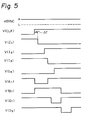
- Figure 5 illustrates the waveforms of each portion in case of a high level of the horizontal synchronizing signal H sync.
- the waveforms of the input clock signal CLK and the output of each inverter I 1 , I 2 , I 3 , I4 are delayed by the time AT of one of the inverters, for instance, 10 nsec.
- the output of the NAND gate A l is a low level only in the case of a high level of potential in both CLK and the output of I3.
- the SR flip-flop FF 1 composed of the NAND gates B 1 and C 1 is set at the declining time of the A 1 output signal, so the potential of the outputting point of the SR flip-flop, i.e, that of the B 1 output, is raised in response to the last transition.
- the potential of the output of the NAND gate D 1 in the output portion i.e., that of the D 1 output
- the potential of the output of the NAND gate D 1 in the output portion i.e., that of the D 1 output
- the potential of the output of the NAND gate D 1 in the output portion i.e., that of the D 1 output
- the potential of the potential of the B 1 output and I4 output are a high level
- the D 2 output of the second stage of units falls when it is delayed by the equivalent of two gates from the D 1 output of the first stage of units, that is to say, by the equivalent of two inverters. Accordingly, the SR flip-flop of the first stage of units is reset when the D 2 output of the second stage of units falls.
- the B 1 output changes to the low level and the D 1 output changes to the high level. That is to say, the signal of the D 1 output at the first stage of units becomes a pulse of negative polarity having a time duration equivalent to the delay time of two gates.
- the D 2 output of the second stage of units also has a time duration equivalent to a delay time of two gates and becomes a pulse of negative polarity which falls after the D 1 output signal has been risen.
- Figure 6 shows the waveforms of each portion when the horizontal synchronizing signal H sync falls, for instance, at the neighboring point of time when the output of the inverter I 2 , i.e., the I 2 output signal, rises.
- the A output signal i.e., the output of the NAND gate A 1 is the high level when the horizontal synchronizing signal H sync falls.
- the SR flip-flop of the first stage of units is set when the A 1 output signal falls, so, at that time, the B 1 output signal changes from the low level to the high level.
- the potential of D 1 output as the output of the NAND gate D 1 in the output portion changes to the low level when the potential of I4 output rises.
- the output of the NAND gate A 2 in the input portion of the second stage of units is always the high level and, as the output of the SR flip-flop FF 2 composed of the NAND gates B 2 and C 2 remains at the low level, the potential of the D 2 output, i.e., the output of the second stage of units, is held at the high level.
- the SR flip-flop of the first stage of units is not reset when the potential of the D 2 output is a high level, the potential of the D 1 output, i.e., the output of the first stage of units, is kept at the low level.
- Figure 7 illustrates the waveforms of each portion in the vicinity of the horizontal synchronizing signal H sync.
- the outputs of each unit, D l output, D 2 output, and so on have waveforms which change to a low level in sequence by a time equivalent to the delay time per two gates.
- the output V (SEL) of the NAND gate E is a high level over nearly the whole period.
- the output V (SEL) of the NAND gate E is a signal which is the inverted signal of the clock pulse of D 1 output, that is, a signal of clock pulse of I4 output. It is possible to obtain the clock pulse supplied to one input terminal of the NAND gate D 1 in the output portion from a tap of the delay circuit in accordance with a desired phase.
- the clock pulse which has the nearest leading edge timing to the point of time of the trailing edge before the time when the following horizontal synchronizing signal H sync falls is selected and the signal V (I4) output is as K out.
- the delay time of the delay circuit needs to be one period of time of the clock pulse.
- the number of gates in the plurality of inverters which constitute the delay circuit should be selected in consideration of the extent of operation and the allowance of phase error between the external signal and the output signal.
- multi-stage inverters are employed in the delay circuit. It is not always necessary that the number of stages of multi-stage inverters be large, for instance, when applied to a CRT controller and the like. As long as the phase error creates no unnatural feature on the display screen, the number of stages of the multi-stage inverters in the delay circuit can be kept to a moderate extent and comparatively simple circuitry is sufficient.
- phase synchronizing circuit in accordance with the present invention may be applicable to display of channel numbers in a television display controller (TVDC) to denote the channel number and the like on the screen of a picture tube.
- TVDC television display controller
Landscapes
- Synchronizing For Television (AREA)
- Stabilization Of Oscillater, Synchronisation, Frequency Synthesizers (AREA)
Applications Claiming Priority (2)
| Application Number | Priority Date | Filing Date | Title |
|---|---|---|---|
| JP59059466A JPS60204121A (ja) | 1984-03-29 | 1984-03-29 | 位相同期回路 |
| JP59466/84 | 1984-03-29 |
Publications (3)
| Publication Number | Publication Date |
|---|---|
| EP0157701A2 true EP0157701A2 (de) | 1985-10-09 |
| EP0157701A3 EP0157701A3 (en) | 1987-09-09 |
| EP0157701B1 EP0157701B1 (de) | 1991-12-27 |
Family
ID=13114112
Family Applications (1)
| Application Number | Title | Priority Date | Filing Date |
|---|---|---|---|
| EP85400616A Expired - Lifetime EP0157701B1 (de) | 1984-03-29 | 1985-03-29 | Phasensynchronisierungsschaltung |
Country Status (4)
| Country | Link |
|---|---|
| US (1) | US4713621A (de) |
| EP (1) | EP0157701B1 (de) |
| JP (1) | JPS60204121A (de) |
| DE (1) | DE3584985D1 (de) |
Cited By (7)
| Publication number | Priority date | Publication date | Assignee | Title |
|---|---|---|---|---|
| EP0208449A3 (en) * | 1985-06-21 | 1988-10-12 | Advanced Micro Devices, Inc. | Apparatus for synchronization of a first signal with a second signal |
| EP0240232A3 (de) * | 1986-04-01 | 1988-11-17 | Hewlett-Packard Company | Digitale Phasenregelschleife |
| EP0317821A3 (de) * | 1987-11-25 | 1990-10-10 | Siemens Aktiengesellschaft | Digitale phasenverriegelte Schleife mit hoher Auflösung |
| EP0326007A3 (de) * | 1988-01-28 | 1990-10-17 | Siemens Aktiengesellschaft | Digitale phasenverriegelte Schleife mit hoher Auflösung für die zentrale Frequenz |
| EP0430480A3 (en) * | 1989-11-13 | 1992-11-25 | Motorola, Inc. | Fsk time-delay demodulator with reduced dc-offset |
| GB2349755A (en) * | 1999-05-07 | 2000-11-08 | Synectix Ltd | Clock signal generator |
| RU2167493C1 (ru) * | 2000-02-07 | 2001-05-20 | Пензенский технологический институт | Устройство синхронизации |
Families Citing this family (54)
| Publication number | Priority date | Publication date | Assignee | Title |
|---|---|---|---|---|
| US4796095A (en) * | 1986-09-09 | 1989-01-03 | Rioch Company, Limited | Method of generating image scanning clock signals in optical scanning apparatus |
| US4814879A (en) * | 1987-08-07 | 1989-03-21 | Rca Licensing Corporation | Signal phase alignment circuitry |
| US4868514A (en) * | 1987-11-17 | 1989-09-19 | International Business Machines Corporation | Apparatus and method for digital compensation of oscillator drift |
| JPH01149516A (ja) * | 1987-12-04 | 1989-06-12 | Mitsubishi Electric Corp | クロック発生装置 |
| JPH07114348B2 (ja) * | 1987-12-11 | 1995-12-06 | 日本電気株式会社 | 論理回路 |
| US4965815A (en) * | 1988-07-21 | 1990-10-23 | U.S. Philips Corporation | Phase detection circuit for stepwise measurement of a phase relation |
| JPH0773255B2 (ja) * | 1989-03-17 | 1995-08-02 | 富士通株式会社 | ビット照合制御方式 |
| JPH0732389B2 (ja) * | 1989-09-22 | 1995-04-10 | 日本電気株式会社 | クロツクジツタ抑圧回路 |
| US5015871A (en) * | 1989-11-03 | 1991-05-14 | Harris Corporation | Multiple external asynchronous triggers circuit |
| US5258660A (en) * | 1990-01-16 | 1993-11-02 | Cray Research, Inc. | Skew-compensated clock distribution system |
| JP2868266B2 (ja) * | 1990-01-25 | 1999-03-10 | 株式会社日本自動車部品総合研究所 | 信号位相差検出回路及び信号位相差検出方法 |
| US5073730A (en) * | 1990-04-23 | 1991-12-17 | International Business Machines Corporation | Current transient reduction for vlsi chips |
| US5066868A (en) * | 1990-08-13 | 1991-11-19 | Thomson Consumer Electronics, Inc. | Apparatus for generating phase shifted clock signals |
| US5107264A (en) * | 1990-09-26 | 1992-04-21 | International Business Machines Corporation | Digital frequency multiplication and data serialization circuits |
| DE4142825A1 (de) * | 1990-12-26 | 1992-07-02 | Mitsubishi Electric Corp | Synchronisierter taktgenerator |
| US5291070A (en) * | 1991-01-28 | 1994-03-01 | Advanced Micro Devices, Inc. | Microprocessor synchronous timing system |
| JPH04298116A (ja) * | 1991-03-27 | 1992-10-21 | Toshiba Corp | サンプリング信号発生回路 |
| US5272390A (en) * | 1991-09-23 | 1993-12-21 | Digital Equipment Corporation | Method and apparatus for clock skew reduction through absolute delay regulation |
| US5245231A (en) * | 1991-12-30 | 1993-09-14 | Dell Usa, L.P. | Integrated delay line |
| US5534808A (en) * | 1992-01-31 | 1996-07-09 | Konica Corporation | Signal delay method, signal delay device and circuit for use in the apparatus |
| JP3381938B2 (ja) * | 1992-06-05 | 2003-03-04 | 株式会社東芝 | 入力遷移検知パルス発生回路 |
| SE515076C2 (sv) * | 1992-07-01 | 2001-06-05 | Ericsson Telefon Ab L M | Multiplexor-/demultiplexorkrets |
| US5404437A (en) * | 1992-11-10 | 1995-04-04 | Sigma Designs, Inc. | Mixing of computer graphics and animation sequences |
| JP3247190B2 (ja) * | 1993-04-13 | 2002-01-15 | 三菱電機株式会社 | 位相同期回路および集積回路装置 |
| US5587675A (en) * | 1993-08-12 | 1996-12-24 | At&T Global Information Solutions Company | Multiclock controller |
| US5598576A (en) * | 1994-03-30 | 1997-01-28 | Sigma Designs, Incorporated | Audio output device having digital signal processor for responding to commands issued by processor by emulating designated functions according to common command interface |
| US5515107A (en) * | 1994-03-30 | 1996-05-07 | Sigma Designs, Incorporated | Method of encoding a stream of motion picture data |
| JP2830735B2 (ja) * | 1994-04-19 | 1998-12-02 | 日本電気株式会社 | 位相同期型タイミング発生回路 |
| JP3553639B2 (ja) * | 1994-05-12 | 2004-08-11 | アジレント・テクノロジーズ・インク | タイミング調整回路 |
| US5689530A (en) * | 1994-06-22 | 1997-11-18 | Alcatel Network Systems, Inc. | Data recovery circuit with large retime margin |
| US5592519A (en) * | 1994-06-22 | 1997-01-07 | Alcatel Network Systems, Inc. | Dual frequency clock recovery using common multitap line |
| US5528309A (en) | 1994-06-28 | 1996-06-18 | Sigma Designs, Incorporated | Analog video chromakey mixer |
| US6124897A (en) * | 1996-09-30 | 2000-09-26 | Sigma Designs, Inc. | Method and apparatus for automatic calibration of analog video chromakey mixer |
| JP3461944B2 (ja) * | 1994-12-26 | 2003-10-27 | 富士通株式会社 | パルス信号整形回路 |
| US6239627B1 (en) * | 1995-01-03 | 2001-05-29 | Via-Cyrix, Inc. | Clock multiplier using nonoverlapping clock pulses for waveform generation |
| WO1997005739A1 (en) * | 1995-08-01 | 1997-02-13 | Auravision Corporation | Transition aligned video synchronization system |
| US5663767A (en) * | 1995-10-25 | 1997-09-02 | Thomson Consumer Electronics, Inc. | Clock re-timing apparatus with cascaded delay stages |
| KR0179779B1 (ko) * | 1995-12-18 | 1999-04-01 | 문정환 | 클럭신호 모델링 회로 |
| US5945861A (en) * | 1995-12-18 | 1999-08-31 | Lg Semicon., Co. Ltd. | Clock signal modeling circuit with negative delay |
| US5719511A (en) * | 1996-01-31 | 1998-02-17 | Sigma Designs, Inc. | Circuit for generating an output signal synchronized to an input signal |
| US5818468A (en) * | 1996-06-04 | 1998-10-06 | Sigma Designs, Inc. | Decoding video signals at high speed using a memory buffer |
| US6128726A (en) | 1996-06-04 | 2000-10-03 | Sigma Designs, Inc. | Accurate high speed digital signal processor |
| US5959481A (en) * | 1997-02-18 | 1999-09-28 | Rambus Inc. | Bus driver circuit including a slew rate indicator circuit having a one shot circuit |
| US6154079A (en) * | 1997-06-12 | 2000-11-28 | Lg Semicon Co., Ltd. | Negative delay circuit operable in wide band frequency |
| US6184936B1 (en) | 1997-10-06 | 2001-02-06 | Sigma Designs, Inc. | Multi-function USB capture chip using bufferless data compression |
| US6690834B1 (en) | 1999-01-22 | 2004-02-10 | Sigma Designs, Inc. | Compression of pixel data |
| US6675297B1 (en) | 1999-03-01 | 2004-01-06 | Sigma Designs, Inc. | Method and apparatus for generating and using a tamper-resistant encryption key |
| US6687770B1 (en) | 1999-03-08 | 2004-02-03 | Sigma Designs, Inc. | Controlling consumption of time-stamped information by a buffered system |
| CA2270516C (en) * | 1999-04-30 | 2009-11-17 | Mosaid Technologies Incorporated | Frequency-doubling delay locked loop |
| US6654956B1 (en) | 2000-04-10 | 2003-11-25 | Sigma Designs, Inc. | Method, apparatus and computer program product for synchronizing presentation of digital video data with serving of digital video data |
| US6441666B1 (en) * | 2000-07-20 | 2002-08-27 | Silicon Graphics, Inc. | System and method for generating clock signals |
| US6704882B2 (en) | 2001-01-22 | 2004-03-09 | Mayo Foundation For Medical Education And Research | Data bit-to-clock alignment circuit with first bit capture capability |
| US7120215B2 (en) * | 2001-12-12 | 2006-10-10 | Via Technologies, Inc. | Apparatus and method for on-chip jitter measurement |
| US7680618B2 (en) * | 2007-09-28 | 2010-03-16 | Tektronix, Inc. | Random edge calibration of oversampling digital acquisition system |
Family Cites Families (11)
| Publication number | Priority date | Publication date | Assignee | Title |
|---|---|---|---|---|
| US3024417A (en) * | 1960-01-07 | 1962-03-06 | Collins Radio Co | Proportional digital synchronizer |
| FR1277331A (fr) * | 1960-10-17 | 1961-12-01 | Central De Telecomm Sa Lab | Perfectionnements aux dispositifs de régénération d'impulsions |
| US3502991A (en) * | 1967-06-19 | 1970-03-24 | Bell Telephone Labor Inc | Signal generator with asynchronous start |
| US3624519A (en) * | 1969-11-10 | 1971-11-30 | Westinghouse Electric Corp | Tapped delay line timing circuit |
| US4061975A (en) * | 1973-04-11 | 1977-12-06 | Nippon Steel Corporation | Receiver for pulses of different widths |
| FR2313827A1 (fr) * | 1975-06-02 | 1976-12-31 | Materiel Telephonique | Systeme de transmission de suites d'elements binaires |
| US4023110A (en) * | 1975-12-04 | 1977-05-10 | The United States Of America As Represented By The Secretary Of The Army | Pulse comparison system |
| FR2459585A1 (fr) * | 1979-06-20 | 1981-01-09 | Thomson Csf | Procede et dispositif pour l'affinage de la remise en phase d'une horloge locale |
| NL183214C (nl) * | 1980-01-31 | 1988-08-16 | Philips Nv | Inrichting voor het synchroniseren van de fase van een lokaal opgewekt kloksignaal met de fase van een ingangssignaal. |
| JPS58202680A (ja) * | 1982-05-21 | 1983-11-25 | Toshiba Corp | 位相同期回路 |
| DE3582914D1 (de) * | 1984-10-31 | 1991-06-27 | Rca Licensing Corp | Fernsehanzeigeanordnung umfassend einen zeichengenerator mit einem nicht mit der zeilenfrequenz synchronisierten taktgeber. |
-
1984
- 1984-03-29 JP JP59059466A patent/JPS60204121A/ja active Pending
-
1985
- 1985-03-28 US US06/717,198 patent/US4713621A/en not_active Expired - Fee Related
- 1985-03-29 EP EP85400616A patent/EP0157701B1/de not_active Expired - Lifetime
- 1985-03-29 DE DE8585400616T patent/DE3584985D1/de not_active Expired - Lifetime
Cited By (8)
| Publication number | Priority date | Publication date | Assignee | Title |
|---|---|---|---|---|
| EP0208449A3 (en) * | 1985-06-21 | 1988-10-12 | Advanced Micro Devices, Inc. | Apparatus for synchronization of a first signal with a second signal |
| EP0240232A3 (de) * | 1986-04-01 | 1988-11-17 | Hewlett-Packard Company | Digitale Phasenregelschleife |
| EP0317821A3 (de) * | 1987-11-25 | 1990-10-10 | Siemens Aktiengesellschaft | Digitale phasenverriegelte Schleife mit hoher Auflösung |
| EP0326007A3 (de) * | 1988-01-28 | 1990-10-17 | Siemens Aktiengesellschaft | Digitale phasenverriegelte Schleife mit hoher Auflösung für die zentrale Frequenz |
| EP0430480A3 (en) * | 1989-11-13 | 1992-11-25 | Motorola, Inc. | Fsk time-delay demodulator with reduced dc-offset |
| GB2349755A (en) * | 1999-05-07 | 2000-11-08 | Synectix Ltd | Clock signal generator |
| GB2349755B (en) * | 1999-05-07 | 2003-05-14 | Synectix Ltd | Clock signal generator |
| RU2167493C1 (ru) * | 2000-02-07 | 2001-05-20 | Пензенский технологический институт | Устройство синхронизации |
Also Published As
| Publication number | Publication date |
|---|---|
| US4713621A (en) | 1987-12-15 |
| DE3584985D1 (de) | 1992-02-06 |
| EP0157701A3 (en) | 1987-09-09 |
| EP0157701B1 (de) | 1991-12-27 |
| JPS60204121A (ja) | 1985-10-15 |
Similar Documents
| Publication | Publication Date | Title |
|---|---|---|
| US4713621A (en) | Phase synchronization circuit | |
| US4408198A (en) | Video character generator | |
| EP0178429A2 (de) | Zeitimpulsgenerator zur Erzeugung von mit dem horizontalen Videosynchronisationssignal synchronisierten Zeitimpulsen | |
| EP0419161A2 (de) | Schaltung zur Unterdrückung eines Taktflatterns | |
| US4623925A (en) | Television receiver having character generator with non-line locked clock oscillator | |
| JPS581785B2 (ja) | 陰極線管の表示装置 | |
| US4970588A (en) | Video monitoring apparatus with plural inputs | |
| US10909906B2 (en) | Display device | |
| JPH02301269A (ja) | キー信号遅延装置 | |
| US6404833B1 (en) | Digital phase synchronizing apparatus | |
| KR890004217B1 (ko) | 위상동기회로 | |
| US5015871A (en) | Multiple external asynchronous triggers circuit | |
| EP0358275A1 (de) | Scheinbar zeilensynchronisierter Schreibtakt für Bild-im-Bild-Videoanwendungen | |
| JP2001331157A (ja) | 映像信号変換装置 | |
| EP0520223A2 (de) | Bildanzeigevorrichtung | |
| EP0416465B1 (de) | Synchronisationskompensierungsschaltung zur Anwendung in einer Abtastwiedergabeschaltung | |
| KR100721805B1 (ko) | 수평 afc 회로 | |
| JP3157554B2 (ja) | 半導体遅延線装置とその駆動方法 | |
| JPH0421393B2 (de) | ||
| JP2642108B2 (ja) | 同期回路 | |
| KR910007193Y1 (ko) | 자화면의 디스플레이 스타트 포인트 가변회로 | |
| JPH03263976A (ja) | 同期分離回路 | |
| JP2000244768A (ja) | 映像信号処理回路 | |
| JP2000278552A (ja) | 画像表示制御方法および装置 | |
| JPS5857116B2 (ja) | 陰極線管表示装置の制御回路 |
Legal Events
| Date | Code | Title | Description |
|---|---|---|---|
| PUAI | Public reference made under article 153(3) epc to a published international application that has entered the european phase |
Free format text: ORIGINAL CODE: 0009012 |
|
| AK | Designated contracting states |
Designated state(s): DE FR GB |
|
| RIN1 | Information on inventor provided before grant (corrected) |
Inventor name: TEMPAKU, JUNYA Inventor name: NAKAMURA, HARUHIKO |
|
| PUAL | Search report despatched |
Free format text: ORIGINAL CODE: 0009013 |
|
| AK | Designated contracting states |
Kind code of ref document: A3 Designated state(s): DE FR GB |
|
| 17P | Request for examination filed |
Effective date: 19880122 |
|
| 17Q | First examination report despatched |
Effective date: 19900425 |
|
| GRAA | (expected) grant |
Free format text: ORIGINAL CODE: 0009210 |
|
| AK | Designated contracting states |
Kind code of ref document: B1 Designated state(s): DE FR GB |
|
| REF | Corresponds to: |
Ref document number: 3584985 Country of ref document: DE Date of ref document: 19920206 |
|
| ET | Fr: translation filed | ||
| PLBE | No opposition filed within time limit |
Free format text: ORIGINAL CODE: 0009261 |
|
| STAA | Information on the status of an ep patent application or granted ep patent |
Free format text: STATUS: NO OPPOSITION FILED WITHIN TIME LIMIT |
|
| 26N | No opposition filed | ||
| PGFP | Annual fee paid to national office [announced via postgrant information from national office to epo] |
Ref country code: GB Payment date: 19930105 Year of fee payment: 9 |
|
| PGFP | Annual fee paid to national office [announced via postgrant information from national office to epo] |
Ref country code: FR Payment date: 19930330 Year of fee payment: 9 |
|
| PGFP | Annual fee paid to national office [announced via postgrant information from national office to epo] |
Ref country code: DE Payment date: 19930521 Year of fee payment: 9 |
|
| PG25 | Lapsed in a contracting state [announced via postgrant information from national office to epo] |
Ref country code: GB Effective date: 19940329 |
|
| GBPC | Gb: european patent ceased through non-payment of renewal fee |
Effective date: 19940329 |
|
| PG25 | Lapsed in a contracting state [announced via postgrant information from national office to epo] |
Ref country code: FR Effective date: 19941130 |
|
| PG25 | Lapsed in a contracting state [announced via postgrant information from national office to epo] |
Ref country code: DE Effective date: 19941201 |
|
| REG | Reference to a national code |
Ref country code: FR Ref legal event code: ST |