EP0146005A2 - Appareil pour la détection de défauts de surface - Google Patents
Appareil pour la détection de défauts de surface Download PDFInfo
- Publication number
- EP0146005A2 EP0146005A2 EP84114161A EP84114161A EP0146005A2 EP 0146005 A2 EP0146005 A2 EP 0146005A2 EP 84114161 A EP84114161 A EP 84114161A EP 84114161 A EP84114161 A EP 84114161A EP 0146005 A2 EP0146005 A2 EP 0146005A2
- Authority
- EP
- European Patent Office
- Prior art keywords
- mean value
- laser beam
- data
- digital
- photo
- Prior art date
- Legal status (The legal status is an assumption and is not a legal conclusion. Google has not performed a legal analysis and makes no representation as to the accuracy of the status listed.)
- Granted
Links
- 230000007547 defect Effects 0.000 title claims abstract description 135
- 238000007689 inspection Methods 0.000 claims abstract description 34
- 230000003287 optical effect Effects 0.000 claims description 17
- 239000004065 semiconductor Substances 0.000 claims description 16
- 238000000034 method Methods 0.000 claims description 4
- 230000008569 process Effects 0.000 claims description 4
- 230000004044 response Effects 0.000 claims description 4
- 238000006243 chemical reaction Methods 0.000 claims description 2
- 230000007246 mechanism Effects 0.000 abstract description 11
- 235000012431 wafers Nutrition 0.000 description 41
- 238000005070 sampling Methods 0.000 description 25
- 238000012545 processing Methods 0.000 description 19
- 239000000428 dust Substances 0.000 description 5
- 238000004519 manufacturing process Methods 0.000 description 5
- 230000035945 sensitivity Effects 0.000 description 4
- 238000011109 contamination Methods 0.000 description 3
- 230000002950 deficient Effects 0.000 description 3
- 238000001514 detection method Methods 0.000 description 3
- 238000009792 diffusion process Methods 0.000 description 3
- 230000000694 effects Effects 0.000 description 3
- CPLXHLVBOLITMK-UHFFFAOYSA-N magnesium oxide Inorganic materials [Mg]=O CPLXHLVBOLITMK-UHFFFAOYSA-N 0.000 description 3
- 239000000395 magnesium oxide Substances 0.000 description 3
- AXZKOIWUVFPNLO-UHFFFAOYSA-N magnesium;oxygen(2-) Chemical compound [O-2].[Mg+2] AXZKOIWUVFPNLO-UHFFFAOYSA-N 0.000 description 3
- 239000013074 reference sample Substances 0.000 description 3
- 238000012546 transfer Methods 0.000 description 3
- TZCXTZWJZNENPQ-UHFFFAOYSA-L barium sulfate Chemical compound [Ba+2].[O-]S([O-])(=O)=O TZCXTZWJZNENPQ-UHFFFAOYSA-L 0.000 description 2
- 238000011156 evaluation Methods 0.000 description 2
- 239000013307 optical fiber Substances 0.000 description 2
- 238000011179 visual inspection Methods 0.000 description 2
- XUIMIQQOPSSXEZ-UHFFFAOYSA-N Silicon Chemical compound [Si] XUIMIQQOPSSXEZ-UHFFFAOYSA-N 0.000 description 1
- 230000032683 aging Effects 0.000 description 1
- 238000013480 data collection Methods 0.000 description 1
- 238000012986 modification Methods 0.000 description 1
- 230000004048 modification Effects 0.000 description 1
- 239000002245 particle Substances 0.000 description 1
- 230000002093 peripheral effect Effects 0.000 description 1
- 229920002120 photoresistant polymer Polymers 0.000 description 1
- 229910021420 polycrystalline silicon Inorganic materials 0.000 description 1
- 229910052710 silicon Inorganic materials 0.000 description 1
- 239000010703 silicon Substances 0.000 description 1
Images


Classifications
-
- G—PHYSICS
- G01—MEASURING; TESTING
- G01N—INVESTIGATING OR ANALYSING MATERIALS BY DETERMINING THEIR CHEMICAL OR PHYSICAL PROPERTIES
- G01N21/00—Investigating or analysing materials by the use of optical means, i.e. using sub-millimetre waves, infrared, visible or ultraviolet light
- G01N21/84—Systems specially adapted for particular applications
- G01N21/88—Investigating the presence of flaws or contamination
- G01N21/95—Investigating the presence of flaws or contamination characterised by the material or shape of the object to be examined
- G01N21/9501—Semiconductor wafers
-
- G—PHYSICS
- G01—MEASURING; TESTING
- G01N—INVESTIGATING OR ANALYSING MATERIALS BY DETERMINING THEIR CHEMICAL OR PHYSICAL PROPERTIES
- G01N21/00—Investigating or analysing materials by the use of optical means, i.e. using sub-millimetre waves, infrared, visible or ultraviolet light
- G01N21/84—Systems specially adapted for particular applications
- G01N21/88—Investigating the presence of flaws or contamination
- G01N21/94—Investigating contamination, e.g. dust
-
- G—PHYSICS
- G01—MEASURING; TESTING
- G01N—INVESTIGATING OR ANALYSING MATERIALS BY DETERMINING THEIR CHEMICAL OR PHYSICAL PROPERTIES
- G01N2201/00—Features of devices classified in G01N21/00
- G01N2201/06—Illumination; Optics
- G01N2201/065—Integrating spheres
-
- G—PHYSICS
- G01—MEASURING; TESTING
- G01N—INVESTIGATING OR ANALYSING MATERIALS BY DETERMINING THEIR CHEMICAL OR PHYSICAL PROPERTIES
- G01N2201/00—Features of devices classified in G01N21/00
- G01N2201/10—Scanning
- G01N2201/104—Mechano-optical scan, i.e. object and beam moving
- G01N2201/1045—Spiral scan
Definitions
- This invention relates to an apparatus for inspecting an object for defects on the surface thereof, and more particularly to an apparatus for inspecting a semiconductor wafer for defect or defects, for example, contamination, dust, scratches, etc. on the wafer surface.
- the results of the inspections usually differ with inspecting persons. Therefore, the inspection results can not be used for quantitativing the results to find or detect defect or defects on the wafer surface.
- the recent integrated circuits have been miniaturized in size more and more, and actually it is required to discriminate 1 ⁇ m or less of the surface defect size for exact evaluation of the semiconductor manufacturing process. It is impossible, however, to discriminate such a minute size by a visual inspection.
- the surface of a semiconductor wafer is illuminated with light beam 3 from an incandescent light source or a laser source, as shown in Fig. 1.
- a regular reflecting light 4 and the scattered light 5 are sensed by photo-electric converters 6 and 6.
- the output voltages from the photo-electric converters 6 and 6 are compared with one or more threshold voltages to detect defect, e.g., contamination, dust, or scratch on the wafer surface, and to discriminate the size of the defect.
- a fixed threshold level VT is set up for the defect detection.
- Different wafers under inspection provide different output signal levels, respectively.
- a semiconductor wafer with a mirror surface produces an output signal V I .
- a film formed wafer provides an output signal V II . Therefore, the threshold level must be changed for each wafer under inspection, and the threshold level must be experimentally determined.
- the setting of the threshold level is troublesome and time-consuming work. In the case of a warped semiconductor wafer, the same problem arises.
- the sizes of defects as detected and classified can not be used for quantitative processing purposes. Therefore, it is necessary to calibrate the defect size data by a reference sample every time the data are collected.
- an object of the present invention to provide a new and improved apparatus which quantitatively, quickly and accurately inspects an object for defects on the surface thereof, without experimentally setting up threshold levels or calibrating the collected data of surface defects.
- an apparatus for inspecting an object under inspection for defects on the surface thereof comprising means for holding the object under inspection in a manner that the substantially entire surface of the object may relatively be scanned by laser beam, spherical integrating light collecting means provided at one end with an opening as is disposed close to the inspected surface of the object held by the holding means, laser beam illuminating means coupled with other end of the spherical integrating light collecting means and for illuminating the inspected surface of the object with the laser beam through the opening, photo-electric converting means for receiving the scattered light as is reflected by the inspected surface and collected by the spherical integrating light collecting means, and for converting the scattered light into an electrical signal representing an amount of light, analog to digital converting means for converting analog to digital the electrical signal derived from the photo-electric converting means into a digital signal, peak detecting means for receiving the digital signal derived from the analog to digital converting means to detect peak values at predetermined periods, means for calculating a mean value
- FIG. 3 illustrating a first embodiment of an apparatus for inspecting an object under inspection, for example, a semiconductor wafer, for defect or defects on the surface thereof (referred to as a surface defect inspecting apparatus).
- an illuminating section 8 is comprised of a laser source 9, and a lens system 11 for optically processing laser beams generated from the laser source 9 and spotting the surface of an object 10 with the laser beam.
- a photo sensing section 12 located right under the illuminating section 8 includes a spherical integrating light collector 13 and a photo-electric converter 14 buried in the light collector 13.
- the light collector 13 is used for collecting rays of light scattered by defects on the surface of the object 10, and has a spherical inner surface scattering made of magnesium oxide, for example.
- the object 10 is removably placed on a turntable 16 as a part of a scanning section 15 by a means (not shown), for example, a vacuum chuck.
- the photo-electric converter 14 converts the collected scattered light into an electric signal, and may be a photo multiplier, a photo transistor, a photo diode, or the like.
- the turntable 16 is comprised of a DC motor 18 directly coupled with the turntable 16 for its rotation, a rotary encoder 19 for producing a rotation start signal Rs and a rotating position signal Rp, which are for the turntable 16 and a stepping motor 20 for radially moving the turntable 16 track by track, as will be given later.
- the DC motor 18 and the stepping motor 20 are driven under control of control signals derived from a operation control unit 21 installed separately from the scanning section 15. Through the operation of the motors, the entire surface of the object 10 is coaxial scanned by the laser beam.
- the stepping motor 20 is connected to the operation control unit 21, through a stepping motor control circuit 22.
- the rotary encoder 19 is connected to an address generating circuit 23 and an analog to digital (A/D) converter 24.
- the A/D converter 24 converts the output voltage signal output from the photo-electric converter 14 in the photo sensing section 12 into a digital signal.
- the output of the A/D converter 24 is connected to the input of a comparator 25 through a by-path circuit 26 made up of a switching element.
- the comparator 25 compares between the digital signals converted at every consecutive ten points, and successively produces maximum values, or peak values, of the compared ones.
- the output of the comparator 25 is connected to a memory circuit 27 for scattered light data.
- the input of the memory circuit 27 is connected to the output of the address generating circuit 23 for storing the scattered light data corresponding to a rotation and a moving position of the turntable 16.
- the input of the address generating circuit 23, together with the rotary encoder 19, is connected to the output of the stepping motor control circuit 22.
- the output of the A/D converter 24 is connected to the input of the memory circuit 27, by way of the by-path circuit 26.
- the address generating circuit 23, the A/D converter 24, the comparator 25, the by-path circuit 26, and the memory circuit 27 make up a temporary memory 28.
- the memory circuit 27 is connected to the control unit 21 made up of a microcomputer, for example, and is controlled by the operation control unit 21 for reading and writing of data.
- the operation control unit 21 is connected to the by-path circuit 26, the address generating circuit 23, the DC motor 18 and the stepping motor control circuit 22, and supplies control signals to these circuits.
- the operation control unit 21 is connected to a data memory 29 for storing a program for data processing and the sizes of defects as classified.
- the data memory 29, together with the operation control unit 21, forms a data processing unit 30.
- the operation control unit 21 is connected to a display section 31 including a cathode ray tube (CRT) for visually displaying a distribution of defects on the surface of the object 10 and the number of defects as classified for each size.
- CTR cathode ray tube
- the laser light is reformed into a fine spot beam through the lens system 11, so that it is ready for spotting the surface of the object 10.
- the light collector 13 and the photo-electric converter 14 for detecting the scattered light from the object 10 are also operated so as to be ready for sensing the scattered light.
- the regular reflecting light component from the object 10 is split by a half-mirror (not shown) disposed between the lens system 11 and the light collector 13, for example.
- a step Sl the object 10 is placed on the turntable 16 and fixed thereto by a fixing means (for example, a vacuum chuck).
- the stepping motor 20 is driven by a signal Cs from the operation control unit 21 applied through the stepping motor control circuit 22.
- the stepping motor 20 is driven to move the turntable 16 in the radial direction. Then, the turntable 16 is stopped at a position of a specific radius r of the object 10 where is irradiated with laser beam.
- the DC motor 18 for rotating the turntable 16 is rotated by a signal C D from the operation control unit 21.
- the by-path circuit 26 is driven at the position of the radius r; the output of the A/D converter 24 is directly connected to the memory circuit 27.
- the output voltage from the photo-electric converter 14 during the period of one turn of the turntable 16 is subjected to A/D conversion. Then, the A/D converted one is written into the memory circuit 27.
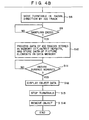
- a step S5 is executed where the operation control unit 21 performs the data processing for obtaining threshold levels T 1 , T 2 and T 3 .
- a step S6 levels L 1 , L 2 and L 3 are set up.
- a mean value V A is added to the respective levels L 1 , L 2 and L3 to set up the threshold levels T l , T 2 and T 3 .
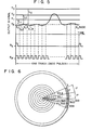
- L l is a level for detecting the smallest surface defect of 1.0 ⁇ m or less, as shown in Fig. 5.
- levels L 2 and L 3 (where L l ⁇ L 2 ⁇ L 3 ) are set up.
- a step S7 by a signal Cs from the control unit 21, the stepping motor 20 is driven to move the turntable 16 in the radial direction. Then, the turntable 16 is stopped at a position where the center of the object 10 is irradiated with the laser beam. For stopping the turntable 16 at that position, a limit switch is mounted thereat and operated when the limit switch is driven. In a step S8, the by-path circuit 26 is driven to connect the A/D converter 24 to the comparator 25. Then, the DC motor 18 is driven to turn the turntable 16.
- the stepping motor 20 is driven to radially move the turntable 16 track by track, a distance of a total of 100 tracks.
- the width of the track is 80 to 90% of a spot diameter d of the laser beam, i.e., 0.8 d to 0.9 d.
- the address generating circuit 23 is also driven by a control signal output from the operation control unit 21.
- the address generating circuit 23 produces an address signal As of a coordinate representing a defect inspecting position on the object, in response to a rotation start signal Rs output from the rotary encoder 19, a rotating position signal Rp and a drive signal output from the stepping motor control circuit 22.
- a step S9 for performing a sampling operation an analog voltage, which is output from the photo-electric converter 14 and varies an intensity of the scattered light, is digitized by the A/D converter 24, every 0.1° in synchronism with the rotating position signal Rp of the rotary encoder 19 directly coupled with the rotary encoder 19.
- the rotating position signal Rp is a pulse signal and contains 3600 pulses for each rotation.
- a maximum of consecutive ten data is taken out by the comparator 25, and output to the memory circuit 27 (see Fig. 6).
- the scattered light data of 100 tracks are stored into a memory a location with a predetermined address of the memory circuit 27.
- the memory circuit 27 stores the maximum data of the scattered light in each area as defined by a center angle of 1°, as shown in Fig. 7.
- Each maximum data consists of a pair of data Yn and 6 (360 data for each rotation x 100 tracks).
- the data stored in the memory circuit 27 are processed so as to form data in which an area of 10 tracks within 1° of the center angle in Fig. 6 is treated as one picture element.
- the data of 100 tracks shown in Fig. 7 are divided into 10 blocks. A maximum value of each block is detected for each rotation, thereby to form the data of one picture element.
- the operation control unit 21 compares the present data with the threshold levels T 1 , T 2 and T 3 , and classifies the data on the basis of the size of the surface defects.
- the classified data is stored into the data memory 29.
- a sequence of the steps Sl to S10 is repeated.
- the operation control unit 21 advances in the flow of control to a step S12.
- the display section 31 visually displays a distribution of surface defects of the object 10 and the number of the surface defects as classified on the basis of the defect size. Such a display by the display section 31 is performed on the basis of the surface defect data from the data memory 29.
- the turntable 16 is stopped in rotation.
- the turntable 16 is returned to a home position.
- the object 10 is removed from the turntable 16. At this point, the inspecting operation of the object 10 ends.
- the surface defect inspecting apparatus works out a mean value V A of the data along a periphery of a circle with the radius r on a location of the surface of the object 10 as properly selected, and a plurality of levels L l to L3 for detecting the surface defects is added to the mean value V A , thereby to form threshold levels T l to T 3 .
- This is commonly done when different objects are inspected, when the object 10 is warped, and when an intensity of the scattered light from a non-defective place of the object 10 varies. Therefore, there is eliminated the need of calibrating the threshold levels with a reference sample for each object.
- the surface defect inspecting apparatus can qualitatively and accurately detect surface defects of the object.
- the calculation of the mean value V A is carried out using part of data not all of the data collected from the surface of the object 10.
- the data of a plurality of tracks are sampled and stored. Then, the surface defects are detected. Further, the data are blocked for each the picture element.
- the temporary memory is provided. Therefore, there is no need for storing all of the data collected from the entire surface of the object. This implies that a memory capacity of the memory is saved. Further, in sampling the data, the comparator 25 obtains the maximum values of ten consecutive data.
- the surface defect inspecting apparatus is applied for inspecting the surface defects of the wafer in manufacturing integrated circuits, inspecting efficiency and accuracy are remarkably improved to greatly contribute to improvements of quality and yield of integrated circuits.
- the laser beam used in the above-mentioned embodiment may be replaced by any type of light, if it is optically sensed by the photo-electric converter.
- the light collector 13 is used for the scattered light sensing in the above-mentioned embodiment, but it may be replaced by any other appropriate means.
- the number of pulses for each rotation in the rotating position signal of the turntable that is, 3600 pulses for each rotation, may appropriately be selected.
- the side face of the turntable is marked black and white, and the reflecting light from the black and white marks is used for data collection.
- the laser beam is moved from the center of the object to the periphery. The direction of the movement of the laser beam may be reversed.
- the calculation of the mean value V A is performed using the data on one periphery of a circle with the specific radius r on the object 10 surface, which is collected before the actual inspection.
- the data on one periphery of the circle with the radius r are selected from the data stored in the memory circuit 27, during an actual inspection.
- the data on the peripheries of circles with different radii may be collected for the mean value calculation.
- the data of 1000 for example, properly selected from all of the data on the object 10 may be used in place of the data on one periphery.
- the mean value V A is calculated using the data properly selected from all of the data on the object 10.
- checking presence or not of surface defects is performed after all of the data are stored into the data memory 29.
- the presence or not of the surface defect may be performed by the operation control unit 21.
- the maximum values of the 10 consecutive data are obtained.
- the number of the data may be any one of the numbers of two or more.
- Fig. 9 shows an arrangement of an overall surface defect inspecting apparatus which is a second embodiment of the present invention.
- the surface defect inspecting apparatus is comprised of a scanning mechanism 109 for illuminating with laser beam an object under inspection 108 as shaped like a disc, such as a semiconductor wafer, a signal processing section 110 for detecting surface defects of the object 108 using a signal output from the scanning mechanism 109, and a signal processing section 110 for visually displaying the result of inspection.
- the scanning mechanism 109 is comprised of a holder 112 for holding the object 108, and an illuminating section 113 for illuminating the object 108 held by the holder 112 with laser beam.
- the holder 112 is comprised of a turntable 114 on which the object 108 is coaxially placed, a bearing member 115 for rotatably supporting the turntable 114, a first motor 116 for rotating the turntable 114 supported by the bearing member 115, a rotary encoder 117 for detecting a rotation of the turntable 114 directly coupled with the first motor 116, a feeding section 118 for moving the bearing member 115 coupled with the bearing member 115 in the radial direction of the object 108 and in a retractible manner, a drive control section 119, and a sucking section 120 for sucking the object 108 on the turntable 114.
- the drive control section 119 controls the feeding section 118 and the first motor 116 to turn the object 108 placed on the turntable 114 by a predetermined amount of turn.
- the turntable 114 is comprised of a disc like shaft 121, and a disc-like table 122 of which the upper surface coaxially coupled with the upper end of the shaft 121 serves as a suction face 114a for the object 108.
- the suction face 114a has a suction hole 123 as a part of the sucking section 120.
- the suction hole 123 axially passes through the shaft 121, and is coupled with a vacuum source (not shown) through a rotary joint (not shown) from the lower side of the shaft 121.
- the feeding section 118 is comprised of a plate 124 suspending from the lower end of the bearing member 115, a feed screw 125 screwed into the plate 124 and having an axial directed in the radial direction of the shaft 121, and a second motor 126.
- the second motor 126 is directly coupled with one end of the feed screw 125 and rotates the feed screw 125 to move the turntable 114 in the direction and in a retractible manner.
- the first and second motors 116 and 126 are rotated by a predetermined amount of turn in response to control signal CD and CS derived from the drive control section 119.
- the illuminating section 113 is comprised of a spherical integrating light collector 127, a laser source 128 and a photo-electric converter 129, as shown in Fig. 10.
- the spherical integrating light collector 127 is cylindrical and is disposed so as to be close to the object 108 fixed to the suction face 114a.
- the light collector 127 is provided with a spherical hollowed section 127b which has a circular opening 127a at the lower end.
- the laser source 128 is coupled at one end with the spherical integrating light collector 127, and obliquely projects laser beam on the object 108, through an opening 127a of the spherical integrating light collector 127.
- the photo-electric converter 129 is coupled with the spherical integrating light collector 127 directly or through an optical fiber (not shown), and receives the scattered laser beam as reflected from the object 108 and collected by the spherical integrating light collector 127, and converts the scattered light into an electrical signal.
- a photomultiplier, a photo transistor, a photo diode, or the like may be used for the photo-electric converter 129.
- the inner surface of the spherical integrating light collector 127 is coated with magnesium oxide to form a diffusion surface 130.
- the upper portion of the spherical integrating light collector 127 is provided with a through-hole 131 allowing the regular reflecting light from the object 108 to pass through to exterior.
- the spherical integrating light collector 127 is also provided with a window 127c. A light sensing portion of the photo-electric converter 129 is fitted to the window 127c.
- the laser source 128 is comprised of a cylindrical optical path member 128a which is connected at one end with the spherical integrating light collector 127 and communicates with a hollowed section 127b of the light collector 127, a cylindrical diaphragm 128b coaxially coupled at one end with the other end of the optical path member 128a, and a laser device 128c mounted to the other end of the diaphragm 128b.
- the diaphragm 128b contains an optical system (not shown) for diaphragming the laser beam output from the laser device 128c.
- An optical axis 128d of the laser beam as " set up by the diaphragm 128b is selected to be oblique to a normal 128e of the object 108 at an angle e.
- the axial line of a through-hole 131 is selected to be oblique to the normal 128e at an angle 8. Therefore, the laser beam generated by the laser device 128c is obliquely incident on the object 108 along the optical axis 128d.
- the regular reflecting light passes through the through-hole 131 to exterior.
- the signal processing section 110 is comprised of the signal processing section 110, an A/D converter 132, a peak detector 133, a mean value calculating unit 134, a sampling control section 135, a first memory section 136, a surface defect classifying section 137, and a central processing section 139.
- the A/D converter 132 converts an analog signal output from the photo-electric converter 129 into a digital signal.
- the peak detector 133 detects a peak value of the digital signal output from the A/D converter 132.
- the mean value calculating unit 134 calculates a mean value of the digital signal output from the A/D converter 132.
- the sampling control section 135 is connected at the input to the rotary encoder 117 and the drive control section 119, and at the output to the peak detector 133 and the mean value calculating unit 134.
- the sampling control section 135 produces a sync signal for sampling the digital signal derived from the A/D converter 132 in the peak detector 133 and the mean value calculating unit 134.
- the first memory section 136 stores a digital signal representing a peak value output from the peak detector 133.
- the surface defect classifying section 137 receives the digital signal of the peak value output from the first memory section 136, detects the surface defect, and classifies the surface defect on the basis of the size of the defects.
- the central processing section 139 is connected through a system bus 138 the mean value calculating unit 134, the sampling control section 135, the surface defect classifying section 137, the first memory section 136, the drive control section 119 and the display section 111, and systematically controls those circuit sections according to a predetermined measuring program.
- the central processing section 139 includes a CPU 140 as a microcomputer for executing various arithmetic operations and controls, and a second memory 141 for controlling a control program for performing an object surface inspection according to a predetermined sequence of procedural steps and the results of inspection.
- the mean value calculated by the mean value calculating unit 134 is set up as a plurality of threshold levels.
- the surface defect classifying section 137 compares the plurality of threshold levels with the peak value output from the peak detector 133. Through the comparison, the surface defect data is extracted for each defect size, and the number of the defect data is counted.
- the display section 111 includes a display 142 and a printer 143.
- the display 142 contains a cathode ray tube (CRT), reads out the inspection result data from the surface defect classifying section 137, and displays a distribution of the surface defects on the object surface, and the number of the defects for each defect size.
- CTR cathode ray tube
- the laser beam is set so that it projects an elliptical spot on the object 108, through the diaphragm 128b.
- the regular reflecting laser beam from the object 108 is emitted outside through the through-hole 131.
- the major axis of the elliptical spot SP of the laser beam is orthogonal to the scanning direction of the object 108 (the peripheral direction), that is, it is set so as to widen the scanning width.
- the scattered laser beams are collected by the diffusion surface 130. Further the spherical integrating light collector 127 for collecting the scattered light and the photo-electric converter 129 are set so as to be ready for the inspection.
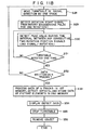
- the object 108 is placed on the table 122 and fixed thereto by the sucking section 120.
- a step S22 the second motor 126 is driven by the signal Cs from the drive control section 119, through the rotation of the feed screw 125, and is moved in the radial direction.
- the table 122 is stopped at a position where the laser beam is projected on a position of the radius r of a circle properly set at the central portion on the object 108.
- the first motor 116 for rotating the table 122 is driven by the signal C D from the drive control section 119. Then, the object 108 is rotated by ten rotations.
- the photo-electric converter 129 produces an analog sensing signal analog detecting signal SA proportional to an amount of the received light for transfer to the A/D converter 132.
- the mean value calculating unit 134 A/D converts the sensing signal analog detecting signal SA, and applies the converted signal SB to the mean value calculating unit 134.
- the rotary encoder 117 produces during the rotation, a rotation start signal Rs and a rotating position signal Rp (360 pulses/rotation) representing a rotating position for transfer to the sampling control section 135.
- the sampling control section 135 produces on the basis of the signals rotation start signal Rs and rotating position signal R, a sampling signal SC corresponding to the rotation of the table 122 for transfer to the mean value calculating unit 134.
- the sampling signal SC is a pulse signal which contains 360 pulse for each rotation of the table 122.
- a step S25 by the mean value calculating unit 134, the sensing signal SB is stored in synchronism with the sampling signal SC. Then, the arithmetic mean value V A of all of the data (X 1 , X 2 , ..., X n ) thus obtained is calculated.
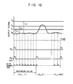
- the mean value V A is temporarily stored in the second memory 141. Then, the CPU 140 adds the levels Ll - L 3 as preset in the second memory 141 corresponding to the size of the surface defects such as dust and scratch to the mean value V A , thereby to provide the threshold levels T1 - T 3 . For example, as shown in Fig.
- T 1 ( V A + Ll ) is a threshold level for detecting the surface defect.
- the levels L 2 and L 3 (where L l ⁇ L 2 ⁇ L 3 ) are set up. These levels L 2 and L 3 are added to the mean value V A , thereby to provide threshold levels T2 and T 3 .
- the threshold levels T 1 to T 3 are transferred via the system bus 138 to the surface defect classifying section 137 and set therein.
- the second motor 126 is driven by the signal Cs from the drive control section 119 to radially move the table 122.
- the table 122 is stopped at a position where the laser beam irradiates the center of the object 108. Such a position is detected by a limit switch (not shown).
- the second motor 126 is driven to move the table 122 by one track in the radial direction. At this time, one track is set at 80 - 90% of the major axis d' of the elliptical spot of the laser light, that is, (0.8 to 0.9) x d'.
- the table 122 is turned in the above-mentioned manner.
- the rotary encoder 117 produces a rotation start signal Rs output at the start of rotation of the table 122, and a rotating position signal Rp containing 360 pulses for each rotation of the table 122.
- These signals rotation start signal Rs and rotating position signal Rp are supplied to the sampling control section 135.
- the sampling control section 135 applies a sampling signal SC containing 360 pulses for each rotation to the peak detector 133.
- analog detecting signal analog detecting signal SA output from the photo-electric converter 129 is digitized into a detecting signal SB.
- the SB is applied to the peak detector 133.
- the peak detector 133 obtains a peak value for each period of the sampling signal SC in synchronism with the sampling signal as input.
- the peak signals detecting signal SD representing the peak values are sequentially applied to the first memory section 136 and stored in predetermined memory locations therein.
- the data (360 data) of one turn of the table 122 is loaded into the first memory section 136.
- the table 122 is further moved by one track in the radial direction. Again, the one turn data is loaded into the memory, by the sampling signal SC.
- a predetermined number n of tracks are scanned in this way.
- the peak value data (Xn, e) are stored in the first memory section 136, as shown in Fig. 14.
- the object 108 For collecting the peak value data from the object 108, the object 108 is segmented into a number of fan-shaped areas by coaxially dividing the object surface and angularly dividing the same by 1°, as shown in Fig. 13.
- the first memory section 136 produces a digital signal representing the peak value data (Xn, ⁇ ) and applies the signal to the surface defect classifying section 137.
- the data larger than the threshold level T 1 are treated as the surface defect data.
- the data larger than the threshold levels T2 and T 3 are treated as the defect data. Further the defect data thus obtained are classified depending on the defect size.
- the CPU 140 converts the polar coordinates into the Cartesian coordinates, and calculates to find what number of the surface defects are contained in the picture element of 1 mm x 1 mm.
- the CPU 140 further drives the display section 111 to display a distribution of the surface defects on the Cartesian coordinates as converted and the number of the surface defects for each defect size.
- the largest surface defect is representatively displayed as the defect data of the picture element.
- the surface defect inspecting apparatus works out a mean value VA of the data along a periphery of a circle with the radius r on a location of the surface of the object 108 as properly selected, and a plurality of levels Ll to L 3 for detecting the surface defects are added to the mean value VA , thereby to form threshold levels T i to T 3 .
- This is commonly done when different object are inspected, when the object 108 is warped, and when an intensity of the scattered light from a non-defective place of the object 108 varies. Therefore, there is eliminated the need of calibrating the threshold levels with a reference sample for each object. Therefore, the surface defect inspecting apparatus can qualitatively and accurately detect surface defects of the object.
- the calculation of the mean value V A is carried out using part of data, not all of the data, collected from the surface of the object 108. Additionally, in the surface defect inspecting apparatus according to the present invention, the data of a plurality of tracks are sampled and stored. Then, the surface defects are detected. Further, the data are blocked for each the picture element. To effect the above, the temporary memory is provided. Therefore, there is no need for storing all of the data collected from the entire surface of the object. This implies that a memory capacity of the memory is saved. When a semiconductor device is used for the laser source, the following effects can be obtained. (1) Approximately 15 mW of the laser output can be obtained. Therefore, an intensity of the scattered light from the object is enough to provide a high sensitivity for the surface defects.
- the semiconductor laser device is smaller in size than the He - Ne laser device, and its power source is smaller than that of the later. It is possible to reduce the illuminating section in size and weight. This feature lessens space occupied by the laser device in a clean room.
- the data is detected at the position of a circle of a specific radius r on the object 108, which are collected before an actual inspection.
- the data collected on the positions of a plurality of radii may be used for the calculation.
- the peak value data from the peak detector 133 derived from the peak detector 133 are temporarily stored in the first memory section 136.
- the peak signal SD is directly applied to the surface defect classifying section 137.
- the surface defects are classified in a real time manner.
- the classified data are loaded into the first memory section 136 or the second memory 141.
- each of the levels Ll - L 3 is added to the mean value V A automatically obtained for each object.
- the levels Li - L 3 may be changed for each object under inspection.
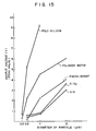
- Fig. 15 illustrating a detecting sensitivity of the surface defect inspecting apparatus when the object is only the polished wafer, it is different from that when the object is a wafer with a film of SiN, Si0 2 , photoresist, or polycrystalline silicon.
- levels (L 1i , L 2 i and L 3 i) are prepared and stored in the data memory 29 or the second memory 141. These levels are read out according to the mean value VA as obtained or by means of a plurality of operation keys.
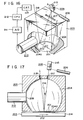
- Figs. 16 and 17 show a third embodiment of a surface defect inspecting apparatus according to the present invention.
- the surface defect inspecting apparatus is comprised of an object placing means 203, a spherical integrating light collector 205, a light source 206, an optical deflecting section 208, a photo-electric converter 210, a A/D converter 211, a data processing unit 212, and a display section 213.
- the object placing means 203 is rectilinearly moved in the direction of arrow 202, while bearing thereon a wafer 201 as an object under inspection.
- the light collector 205 has a hollowed section 204 for collecting the scattered laser beam as is reflected at the wafer right above the object placing means 203.
- the light source 206 generates laser beams.
- the optical deflecting section 208 reflects the laser beam emitted from the light source 206 and moves the laser beam in the direction of arrow 207 orthogonal to the direction of arrow 202, thereby to scan the wafer 201.
- the photo-electric converter 210 is provided with a light receiving surface 209 as a part of the surface of the hollowed section 204.
- the photo-electric converter 210 produces an electrical signal representing an amount of the light received by the light receiving surface 209.
- a photomultiplier, a photo diode, a photo transistor or the like, may be used for the photo-electric converter 210.
- the A/D converter 211 A/D converts the electrical signal from the photo-electric converter 210.
- the data processing unit 212 such as a microcomputer, arithmetically processes the digital signals output from the A/D converter 211 under control of a program preset in a proper memory, and checks the present or not of defects on the wafer surface. This is like that of the first and second embodiments.
- the display section 213 visually displays the results of defect checking by the data processing unit 212.
- the object placing means 203 includes a table 214 on which a wafer 201 is placed at a predetermined location thereon, and a drive mechanism (not shown) for moving the table 214 at a constant speed in the direction of arrow 202, and may be a stepping motor.
- a hollowed section 204 opens at the under surface of the light collector 205.
- the hollowed section 204 has an opening 204a which is circular with an outer diameter slightly larger than the outer diameter of the wafer 201.
- the inner surface of the hollowed section 204 is coated with magnesium oxide or barium sulfate, thereby to form a diffusion surface.
- the optical deflecting section 208 includes a rotating polygonal mirror 215 and a rotating drive mechanism (not shown) for rotating the rotating polygonal mirror 215.
- the rotating axis of the rotating polygonal mirror 215 is arranged in such a manner that the laser beam reflected by the rotating polygonal mirror 215 moves for scan at the maximum diameter portion of the opening 204a in the direction of arrow 207, and at an angle 0 with respect to the normal upstanding on the major surface of the wafer 201.
- a plane through which laser beam reflected by the rotating polygonal mirror 215 passes (this plane is orthogonal to the rotating axis of the rotating polygonal mirror 215) is slanted at an angle 8 with respect to a plane containing the normal line on the major surface of the wafer in the direction of arrow 207, or the scanning locus, and in the scanning direction at the center of the opening 204a.
- the number of the reflecting faces of the rotating polygonal mirror 2L5 is so selected that the scanning distance is equal to the inner diameter of the opening 204a. Such a number is, for example, 18.
- the light source 206 contains a laser oscillator.
- An optical axis of the laser beam oscillated in and emitted from the light source 206 is normal to a line parallel to the rotating axis of the rotating polygonal mirror 215, while satisfying the scanning condition on the major surface of the wafer 201.
- An incoming slit 217 provides a path through which the laser beam reflected by the rotating polygonal mirror 215 enters into the hollowed section 204.
- An outgoing slit 218, crossing the light collector 205 at the substantially center thereof, provides a path through which of the laser beam has scanned the wafer surface. Only the regular reflecting light is led to exterior.
- the incoming slit 217 and the outgoing slit 218 are disposed symmetrically with respect to the surface 216.
- the wafer 201 is placed on the turntable 214.
- the object placing means 203 is driven to position the wafer 201 at the location closer to one's side than the center line of the opening 204a.
- the drive mechanism feeds the table 214 at 400 mm/sec in the direction of arrow 202.
- the laser beam is emitted from the light source 206.
- the rotating drive mechanism in the optical deflecting section 208 is driven to rotate the rotating polygonal mirror 215 at 3600 turns/min. in the direction of arrow A.
- the laser beam from the light source 206 is deflected by the rotating polygonal mirror 215, and reaches the upper surface of the table 214 through the incoming slit 217.
- the laser beam at the upper surface of the table 214 is moved for scan at the maximum diameter portion of the opening 204a in the direction of arrow 207.
- the wafer 201 is scanned by the laser beam at a high speed in the direction of arrow 207. In this way, the wafer 201 is successively scanned from the leading and trailing ends, while being moved in the direction of arrow 202.
- the wafer 201 is entirely scanned on the surface by the laser beam. During this scanning operation, of the laser beams reflected by the wafer 201, the regular reflecting laser beams are led to exterior completely.
- the reflecting laser beams contain scattered reflecting laser beams.
- the scattered reflecting light is collected, by the inner surface of the opening 204a as the scattered reflecting surface, onto the light receiving surface 209. Then, it is converted into an electrical signal containing an amount of the received light, by the photo-electric converter 210.
- the electrical signal output from the photo-electric converter 210 is digitized by the A/D converter 211 and stored into the data processing unit 212.
- the data are stored with an array corresponding to the coordinates applied to the wafer surface illuminated with the laser beam.
- Each data is arithmetically processed for surface defect inspection. For example, in the first and second embodiments as mentioned above, each data is compared with a preset threshold level. The data having a voltage level higher than the threshold level is treated as the data representing a defective position on the wafer surface, and is displayed by the display section 213.
- the wafer surface is scanned at a high speed by the laser beam through the optical deflecting section 208.
- the object placing means 203 bearing the wafer 201 is moved in the direction orthogonal to the scanning direction. Therefore, the entire surface of the wafer 201 can be scanned at high speed and high accuracy.
- Use of the spherical integrating light collector collects only the scattering light due to the surface defect. The thus collected light is used for surface defect detection. This remarkably improves a sensitivity of defect detection.
- the photo-electric converter 210 is directly coupled with the light collector 205, one end of the optical fiber is exposed toward the inner surface of the opening 204a, while the other end thereof is coupled with the photo-electric converter provided separately from the light collector 205.
- a normal light source in place of the laser source, may be used for the light source 206.
- the rotating polygonal mirror 215 in the optical deflecting section 208 may be any optical means if it can move the laser beam at high speed, such as a galvano-mirror.
- the moving direction of the object placing means 203 is not necessarily normal to the laser-moving direction, the direction of arrow 207.
- the object placing means 203 is fixed, while the light source 206, the optical deflecting section 208 and the light collector 205 are kept in a fixed positional relation.
Landscapes
- Physics & Mathematics (AREA)
- Health & Medical Sciences (AREA)
- Life Sciences & Earth Sciences (AREA)
- Chemical & Material Sciences (AREA)
- Analytical Chemistry (AREA)
- Biochemistry (AREA)
- General Health & Medical Sciences (AREA)
- General Physics & Mathematics (AREA)
- Immunology (AREA)
- Pathology (AREA)
- Investigating Materials By The Use Of Optical Means Adapted For Particular Applications (AREA)
Applications Claiming Priority (4)
| Application Number | Priority Date | Filing Date | Title |
|---|---|---|---|
| JP58221394A JPS60113938A (ja) | 1983-11-26 | 1983-11-26 | 表面検査装置 |
| JP221394/83 | 1983-11-26 | ||
| JP148614/84 | 1984-07-19 | ||
| JP14861484A JPS6128846A (ja) | 1984-07-19 | 1984-07-19 | 表面検査装置 |
Publications (3)
| Publication Number | Publication Date |
|---|---|
| EP0146005A2 true EP0146005A2 (fr) | 1985-06-26 |
| EP0146005A3 EP0146005A3 (en) | 1986-05-28 |
| EP0146005B1 EP0146005B1 (fr) | 1991-08-28 |
Family
ID=26478752
Family Applications (1)
| Application Number | Title | Priority Date | Filing Date |
|---|---|---|---|
| EP84114161A Expired EP0146005B1 (fr) | 1983-11-26 | 1984-11-23 | Appareil pour la détection de défauts de surface |
Country Status (3)
| Country | Link |
|---|---|
| US (1) | US4626101A (fr) |
| EP (1) | EP0146005B1 (fr) |
| DE (1) | DE3484982D1 (fr) |
Cited By (3)
| Publication number | Priority date | Publication date | Assignee | Title |
|---|---|---|---|---|
| EP0678911A3 (fr) * | 1994-04-20 | 1996-04-17 | Siemens Ag | Système et appareil pour l'inspection des plaquettes semi-conductrices. |
| NL1006378C2 (nl) * | 1997-06-23 | 1998-12-24 | Tno | Werkwijze en inrichting voor het inspecteren van een voorwerp met betrekking tot verstoringen. |
| CN111197966A (zh) * | 2018-11-16 | 2020-05-26 | 致茂电子(苏州)有限公司 | 使用冷凝手段的表面检测装置及其方法 |
Families Citing this family (58)
| Publication number | Priority date | Publication date | Assignee | Title |
|---|---|---|---|---|
| JPS60235136A (ja) * | 1984-05-09 | 1985-11-21 | Kyodo Printing Co Ltd | 検版方法 |
| DE3667855D1 (de) * | 1985-09-09 | 1990-02-01 | Siemens Ag | Pruefanordnung zur beruehrungslosen ermittlung von defekten in nicht strukturierten flaechen. |
| US4673818A (en) * | 1985-11-25 | 1987-06-16 | Polaroid Corporation | Roughness measuring apparatus |
| DE3620146A1 (de) * | 1986-06-14 | 1987-12-17 | Zeiss Carl Fa | Verfahren zum pruefen von bauteilen aus transparentem material auf oberflaechenfehler und einschluesse |
| DE3620108A1 (de) * | 1986-06-14 | 1987-12-17 | Zeiss Carl Fa | Vorrichtung zum beleuchten von bauteilen aus transparentem material bei der fehlerpruefung |
| US4740708A (en) * | 1987-01-06 | 1988-04-26 | International Business Machines Corporation | Semiconductor wafer surface inspection apparatus and method |
| FR2624608A1 (fr) * | 1987-12-11 | 1989-06-16 | Tech Bois Ameublement Centre | Dispositif de detection automatique de defauts dans un lot heterogene d'objets |
| US4965454A (en) * | 1988-01-21 | 1990-10-23 | Hitachi, Ltd. | Method and apparatus for detecting foreign particle |
| US4875780A (en) * | 1988-02-25 | 1989-10-24 | Eastman Kodak Company | Method and apparatus for inspecting reticles |
| US4873430A (en) * | 1988-10-25 | 1989-10-10 | International Business Machines Corporation | Method and apparatus for optically measuring characteristics of a thin film by directing a P-polarized beam through an integrating sphere at the brewster's angle of the film |
| JPH06105741B2 (ja) * | 1989-11-24 | 1994-12-21 | 株式会社東芝 | インナーリードボンディング検査方法 |
| JP3142852B2 (ja) * | 1990-02-20 | 2001-03-07 | 株式会社日立製作所 | 表面欠陥検査装置 |
| CH681495A5 (fr) * | 1990-03-05 | 1993-03-31 | Tet Techno Investment Trust | |
| US5149978A (en) * | 1990-12-07 | 1992-09-22 | Therma-Wave, Inc. | Apparatus for measuring grain sizes in metalized layers |
| US5256886A (en) * | 1991-04-30 | 1993-10-26 | E. I. Du Pont De Nemours And Company | Apparatus for optically detecting contamination in particles of low optical-loss material |
| US5309339A (en) * | 1992-06-24 | 1994-05-03 | The Schepens Eye Research Institute, Inc. | Concentrator for laser light |
| JP2800587B2 (ja) * | 1992-10-05 | 1998-09-21 | 松下電器産業株式会社 | 異物検査装置および異物検査方法 |
| DE4239456A1 (de) * | 1992-11-24 | 1994-06-09 | Rheinmetall Sick Optical Inspe | Verfahren und Vorrichtung zur Inspektion von Oberflächen |
| US5581346A (en) * | 1993-05-10 | 1996-12-03 | Midwest Research Institute | System for characterizing semiconductor materials and photovoltaic device |
| US5757474A (en) * | 1993-05-10 | 1998-05-26 | Midwest Research Institute | System for characterizing semiconductor materials and photovoltaic devices through calibration |
| US5406367A (en) * | 1993-05-10 | 1995-04-11 | Midwest Research Institute | Defect mapping system |
| JP3482425B2 (ja) * | 1995-03-31 | 2003-12-22 | 株式会社ナノテックス | 検査装置 |
| US5726455A (en) * | 1995-06-30 | 1998-03-10 | Stormedia, Inc. | Disk film optical measurement system |
| US5898181A (en) * | 1995-06-30 | 1999-04-27 | Hdi Instrumentation | Thin film optical measurement system |
| GB9613685D0 (en) * | 1996-06-28 | 1996-08-28 | Crosfield Electronics Ltd | An illumination unit |
| GB2349214B (en) * | 1996-07-18 | 2000-12-20 | Speedfam Ipec Corp | Methods and apparatus for the in-process detection of workpieces |
| US6048745A (en) * | 1997-10-28 | 2000-04-11 | International Business Machines Corporation | Method for mapping scratches in an oxide film |
| US6256093B1 (en) * | 1998-06-25 | 2001-07-03 | Applied Materials, Inc. | On-the-fly automatic defect classification for substrates using signal attributes |
| US6366690B1 (en) * | 1998-07-07 | 2002-04-02 | Applied Materials, Inc. | Pixel based machine for patterned wafers |
| US6324298B1 (en) | 1998-07-15 | 2001-11-27 | August Technology Corp. | Automated wafer defect inspection system and a process of performing such inspection |
| US6882416B1 (en) * | 1999-09-07 | 2005-04-19 | Applied Materials, Inc. | Methods for continuous embedded process monitoring and optical inspection of substrates using specular signature analysis |
| US6721045B1 (en) | 1999-09-07 | 2004-04-13 | Applied Materials, Inc. | Method and apparatus to provide embedded substrate process monitoring through consolidation of multiple process inspection techniques |
| US6693708B1 (en) | 1999-09-07 | 2004-02-17 | Applied Materials, Inc. | Method and apparatus for substrate surface inspection using spectral profiling techniques |
| US6630995B1 (en) | 1999-09-07 | 2003-10-07 | Applied Materials, Inc. | Method and apparatus for embedded substrate and system status monitoring |
| US6707545B1 (en) | 1999-09-07 | 2004-03-16 | Applied Materials, Inc. | Optical signal routing method and apparatus providing multiple inspection collection points on semiconductor manufacturing systems |
| US6707544B1 (en) | 1999-09-07 | 2004-03-16 | Applied Materials, Inc. | Particle detection and embedded vision system to enhance substrate yield and throughput |
| US6813032B1 (en) | 1999-09-07 | 2004-11-02 | Applied Materials, Inc. | Method and apparatus for enhanced embedded substrate inspection through process data collection and substrate imaging techniques |
| US7012684B1 (en) | 1999-09-07 | 2006-03-14 | Applied Materials, Inc. | Method and apparatus to provide for automated process verification and hierarchical substrate examination |
| US6774990B2 (en) * | 2002-08-23 | 2004-08-10 | Intel Corporation | Method to inspect patterns with high resolution photoemission |
| US7002675B2 (en) * | 2003-07-10 | 2006-02-21 | Synetics Solutions, Inc. | Method and apparatus for locating/sizing contaminants on a polished planar surface of a dielectric or semiconductor material |
| JP4391217B2 (ja) * | 2003-12-16 | 2009-12-24 | 株式会社トプコン | 表面検査装置 |
| DE102004020704A1 (de) * | 2004-04-28 | 2005-11-24 | Precitec Kg | Sensorvorrichtung zur Erfassung von Strahlung aus dem Bereich einer Wechselwirkungszone zwischen einem Laserstrahl und einem Werkstück sowie Vorrichtung zur Überwachung eines Laserbearbeitungsvorgangs und Laserbearbeitungskopf |
| WO2006014152A1 (fr) * | 2004-07-01 | 2006-02-09 | Midwest Research Institute | Sonde optique permettant de caracteriser un semiconducteur |
| DE102005019158A1 (de) * | 2005-04-25 | 2006-10-26 | Robert Bosch Gmbh | Punktmessende optische Sensoren |
| JP2007024737A (ja) | 2005-07-20 | 2007-02-01 | Hitachi High-Technologies Corp | 半導体の欠陥検査装置及びその方法 |
| US7319518B2 (en) * | 2005-08-24 | 2008-01-15 | Cree, Inc. | Double side polished wafer scratch inspection tool |
| JP5090041B2 (ja) * | 2006-04-03 | 2012-12-05 | ルネサスエレクトロニクス株式会社 | フォーカス調整方法、その方法を用いた装置、およびその方法に用いられるウェハ |
| DE102008015211B4 (de) * | 2008-03-20 | 2011-01-05 | Infineon Technologies Ag | Messanordnung und Verfahren zum Betreiben der Messanordnung |
| US9163987B2 (en) * | 2010-08-24 | 2015-10-20 | Kla-Tencor Corporation | Defect inspection and photoluminescence measurement system |
| WO2013028196A1 (fr) | 2011-08-25 | 2013-02-28 | Alliance For Sustainable Energy, Llc | Contrôle continu en ligne de la fabrication de photopiles et de piles à combustible faisant appel à une imagerie par réflectance spectrale |
| US8830456B2 (en) | 2013-02-01 | 2014-09-09 | Zeta Instruments, Inc. | Optical inspector |
| US8896825B2 (en) | 2013-02-01 | 2014-11-25 | Zeta Instruments, Inc. | Optical inspector |
| US8836935B1 (en) | 2013-04-12 | 2014-09-16 | Zeta Instruments, Inc. | Optical inspector with selective scattered radiation blocker |
| US8830457B1 (en) | 2013-04-12 | 2014-09-09 | Zeta Instruments, Inc. | Multi-surface optical inspector |
| US8848181B1 (en) | 2013-04-12 | 2014-09-30 | Zeta Instruments, Inc. | Multi-surface scattered radiation differentiation |
| US20170088941A1 (en) * | 2014-05-16 | 2017-03-30 | Applied Materials, Inc. | Apparatus for processing of a material on a substrate and method for measuring optical properties of a material processed on a substrate |
| US10480935B2 (en) | 2016-12-02 | 2019-11-19 | Alliance For Sustainable Energy, Llc | Thickness mapping using multispectral imaging |
| CN113686903B (zh) * | 2021-09-17 | 2024-09-10 | 中国工程物理研究院激光聚变研究中心 | 一种光学元件缺陷检测系统及检测方法 |
Citations (5)
| Publication number | Priority date | Publication date | Assignee | Title |
|---|---|---|---|---|
| JPS57163852A (en) * | 1981-03-31 | 1982-10-08 | Matsushita Electric Works Ltd | Detector for sample surface defect |
| US4360275A (en) * | 1980-08-11 | 1982-11-23 | Litton Systems Inc. | Device for measurement of optical scattering |
| EP0065051A2 (fr) * | 1981-05-12 | 1982-11-24 | Eastman Kodak Company | Procédé et dispositif d'inspection de surface par balayage |
| US4378159A (en) * | 1981-03-30 | 1983-03-29 | Tencor Instruments | Scanning contaminant and defect detector |
| US4391524A (en) * | 1981-03-16 | 1983-07-05 | Rca Corporation | Method for determining the quality of light scattering material |
Family Cites Families (2)
| Publication number | Priority date | Publication date | Assignee | Title |
|---|---|---|---|---|
| ATE13594T1 (de) * | 1980-10-17 | 1985-06-15 | Brent Chemicals Int | Verfahren und einrichtung zum pruefen von einem werkstueck. |
| US4441124A (en) * | 1981-11-05 | 1984-04-03 | Western Electric Company, Inc. | Technique for inspecting semiconductor wafers for particulate contamination |
-
1984
- 1984-11-23 EP EP84114161A patent/EP0146005B1/fr not_active Expired
- 1984-11-23 DE DE8484114161T patent/DE3484982D1/de not_active Expired - Lifetime
- 1984-11-26 US US06/675,008 patent/US4626101A/en not_active Expired - Fee Related
Patent Citations (5)
| Publication number | Priority date | Publication date | Assignee | Title |
|---|---|---|---|---|
| US4360275A (en) * | 1980-08-11 | 1982-11-23 | Litton Systems Inc. | Device for measurement of optical scattering |
| US4391524A (en) * | 1981-03-16 | 1983-07-05 | Rca Corporation | Method for determining the quality of light scattering material |
| US4378159A (en) * | 1981-03-30 | 1983-03-29 | Tencor Instruments | Scanning contaminant and defect detector |
| JPS57163852A (en) * | 1981-03-31 | 1982-10-08 | Matsushita Electric Works Ltd | Detector for sample surface defect |
| EP0065051A2 (fr) * | 1981-05-12 | 1982-11-24 | Eastman Kodak Company | Procédé et dispositif d'inspection de surface par balayage |
Non-Patent Citations (1)
| Title |
|---|
| PATENTS ABSTRACTS OF JAPAN, vol. 7, no. 2 (P-166) [1147], 7th January 1983; & JP - A - 57 163 852 (MATSUSHITA DENKO K.K.) 08.10.1982 * |
Cited By (4)
| Publication number | Priority date | Publication date | Assignee | Title |
|---|---|---|---|---|
| EP0678911A3 (fr) * | 1994-04-20 | 1996-04-17 | Siemens Ag | Système et appareil pour l'inspection des plaquettes semi-conductrices. |
| NL1006378C2 (nl) * | 1997-06-23 | 1998-12-24 | Tno | Werkwijze en inrichting voor het inspecteren van een voorwerp met betrekking tot verstoringen. |
| WO1998059236A1 (fr) * | 1997-06-23 | 1998-12-30 | Nederlandse Organisatie Voor Toegepast-Natuurwetenschappelijk Onderzoek Tno | Procede et dispositif servant a inspecter un article afin de rechercher des defauts |
| CN111197966A (zh) * | 2018-11-16 | 2020-05-26 | 致茂电子(苏州)有限公司 | 使用冷凝手段的表面检测装置及其方法 |
Also Published As
| Publication number | Publication date |
|---|---|
| DE3484982D1 (de) | 1991-10-02 |
| EP0146005B1 (fr) | 1991-08-28 |
| US4626101A (en) | 1986-12-02 |
| EP0146005A3 (en) | 1986-05-28 |
Similar Documents
| Publication | Publication Date | Title |
|---|---|---|
| US4626101A (en) | Surface defect inspecting apparatus | |
| JP4023558B2 (ja) | 明視野照明及び暗視野照明を有する自動検査システム | |
| US6366690B1 (en) | Pixel based machine for patterned wafers | |
| JP3801635B2 (ja) | 製品表面の検査システムおよび方法 | |
| US6603542B1 (en) | High sensitivity optical inspection system and method for detecting flaws on a diffractive surface | |
| US7864310B2 (en) | Surface inspection method and surface inspection apparatus | |
| EP0265229A2 (fr) | Méthode et appareil pour la détection de particules | |
| JPH0341785B2 (fr) | ||
| JPH01143945A (ja) | テープ欠陥検出方法 | |
| JPH0431056B2 (fr) | ||
| US5602401A (en) | Data processing system and method for a surface inspection apparatus | |
| JPH067104B2 (ja) | 表面検査装置 | |
| JPH0517482B2 (fr) | ||
| JPH03181848A (ja) | 半導体材料評価装置 | |
| JPH0513459B2 (fr) | ||
| JPS62266444A (ja) | 表面検査装置 | |
| JPH08101135A (ja) | 異物検査装置 | |
| JPS6165146A (ja) | 表面検査装置 | |
| JPS59180313A (ja) | 表面検査装置 | |
| JP3277400B2 (ja) | 光ディスク欠陥検査装置 | |
| JPH063279A (ja) | ハードディスク又はウエハーの検査方法及び検査装置 | |
| JPS62238445A (ja) | 表面検査装置 | |
| JPS60113938A (ja) | 表面検査装置 | |
| JPH07134103A (ja) | 表面検査装置及び表面検査方法 | |
| JPS6315142A (ja) | 欠陥検査装置 |
Legal Events
| Date | Code | Title | Description |
|---|---|---|---|
| PUAI | Public reference made under article 153(3) epc to a published international application that has entered the european phase |
Free format text: ORIGINAL CODE: 0009012 |
|
| 17P | Request for examination filed |
Effective date: 19841220 |
|
| AK | Designated contracting states |
Designated state(s): DE FR GB IT NL |
|
| PUAL | Search report despatched |
Free format text: ORIGINAL CODE: 0009013 |
|
| AK | Designated contracting states |
Kind code of ref document: A3 Designated state(s): DE FR GB IT NL |
|
| 17Q | First examination report despatched |
Effective date: 19900509 |
|
| GRAA | (expected) grant |
Free format text: ORIGINAL CODE: 0009210 |
|
| AK | Designated contracting states |
Kind code of ref document: B1 Designated state(s): DE FR GB IT NL |
|
| REF | Corresponds to: |
Ref document number: 3484982 Country of ref document: DE Date of ref document: 19911002 |
|
| ITF | It: translation for a ep patent filed | ||
| ET | Fr: translation filed | ||
| PLBE | No opposition filed within time limit |
Free format text: ORIGINAL CODE: 0009261 |
|
| STAA | Information on the status of an ep patent application or granted ep patent |
Free format text: STATUS: NO OPPOSITION FILED WITHIN TIME LIMIT |
|
| 26N | No opposition filed | ||
| PGFP | Annual fee paid to national office [announced via postgrant information from national office to epo] |
Ref country code: DE Payment date: 19941123 Year of fee payment: 11 |
|
| PGFP | Annual fee paid to national office [announced via postgrant information from national office to epo] |
Ref country code: FR Payment date: 19951109 Year of fee payment: 12 |
|
| PGFP | Annual fee paid to national office [announced via postgrant information from national office to epo] |
Ref country code: GB Payment date: 19951115 Year of fee payment: 12 |
|
| PGFP | Annual fee paid to national office [announced via postgrant information from national office to epo] |
Ref country code: NL Payment date: 19951129 Year of fee payment: 12 |
|
| PG25 | Lapsed in a contracting state [announced via postgrant information from national office to epo] |
Ref country code: DE Effective date: 19960801 |
|
| PG25 | Lapsed in a contracting state [announced via postgrant information from national office to epo] |
Ref country code: GB Effective date: 19961123 |
|
| PG25 | Lapsed in a contracting state [announced via postgrant information from national office to epo] |
Ref country code: NL Effective date: 19970601 |
|
| GBPC | Gb: european patent ceased through non-payment of renewal fee |
Effective date: 19961123 |
|
| PG25 | Lapsed in a contracting state [announced via postgrant information from national office to epo] |
Ref country code: FR Effective date: 19970731 |
|
| NLV4 | Nl: lapsed or anulled due to non-payment of the annual fee |
Effective date: 19970601 |
|
| REG | Reference to a national code |
Ref country code: FR Ref legal event code: ST |