EP0140509B1 - Méthode LEC et appareil pour la croissance d'un mono-cristal d'un composé semi-conducteur - Google Patents
Méthode LEC et appareil pour la croissance d'un mono-cristal d'un composé semi-conducteur Download PDFInfo
- Publication number
- EP0140509B1 EP0140509B1 EP84305606A EP84305606A EP0140509B1 EP 0140509 B1 EP0140509 B1 EP 0140509B1 EP 84305606 A EP84305606 A EP 84305606A EP 84305606 A EP84305606 A EP 84305606A EP 0140509 B1 EP0140509 B1 EP 0140509B1
- Authority
- EP
- European Patent Office
- Prior art keywords
- crystal
- temperature
- heater
- zone
- growing
- Prior art date
- Legal status (The legal status is an assumption and is not a legal conclusion. Google has not performed a legal analysis and makes no representation as to the accuracy of the status listed.)
- Expired
Links
- 239000013078 crystal Substances 0.000 title claims description 82
- 238000000034 method Methods 0.000 title claims description 28
- 238000001816 cooling Methods 0.000 claims description 43
- 150000001875 compounds Chemical class 0.000 claims description 24
- 229910001218 Gallium arsenide Inorganic materials 0.000 claims description 22
- 238000009826 distribution Methods 0.000 claims description 21
- 239000007788 liquid Substances 0.000 claims description 21
- 239000008393 encapsulating agent Substances 0.000 claims description 18
- 238000010438 heat treatment Methods 0.000 claims description 13
- 239000000155 melt Substances 0.000 claims description 8
- 238000007598 dipping method Methods 0.000 claims description 2
- 239000004065 semiconductor Substances 0.000 claims description 2
- 235000012431 wafers Nutrition 0.000 description 14
- OKTJSMMVPCPJKN-UHFFFAOYSA-N Carbon Chemical compound [C] OKTJSMMVPCPJKN-UHFFFAOYSA-N 0.000 description 6
- 230000007423 decrease Effects 0.000 description 6
- 239000000463 material Substances 0.000 description 6
- 229910052799 carbon Inorganic materials 0.000 description 5
- 238000010586 diagram Methods 0.000 description 5
- 239000007789 gas Substances 0.000 description 5
- 239000007787 solid Substances 0.000 description 5
- 238000009827 uniform distribution Methods 0.000 description 5
- -1 GaAs compound Chemical class 0.000 description 4
- 230000008646 thermal stress Effects 0.000 description 4
- 238000000137 annealing Methods 0.000 description 3
- IJGRMHOSHXDMSA-UHFFFAOYSA-N Atomic nitrogen Chemical compound N#N IJGRMHOSHXDMSA-UHFFFAOYSA-N 0.000 description 2
- 229910052785 arsenic Inorganic materials 0.000 description 2
- 238000006243 chemical reaction Methods 0.000 description 2
- 230000007547 defect Effects 0.000 description 2
- 229910001873 dinitrogen Inorganic materials 0.000 description 2
- 229910052733 gallium Inorganic materials 0.000 description 2
- 238000000227 grinding Methods 0.000 description 2
- 230000017525 heat dissipation Effects 0.000 description 2
- 239000011261 inert gas Substances 0.000 description 2
- 239000007858 starting material Substances 0.000 description 2
- 229910052581 Si3N4 Inorganic materials 0.000 description 1
- 230000015572 biosynthetic process Effects 0.000 description 1
- 239000011248 coating agent Substances 0.000 description 1
- 238000000576 coating method Methods 0.000 description 1
- 238000011109 contamination Methods 0.000 description 1
- 230000005484 gravity Effects 0.000 description 1
- 229910052738 indium Inorganic materials 0.000 description 1
- 238000004519 manufacturing process Methods 0.000 description 1
- 238000005259 measurement Methods 0.000 description 1
- 238000009828 non-uniform distribution Methods 0.000 description 1
- 238000010899 nucleation Methods 0.000 description 1
- 230000005855 radiation Effects 0.000 description 1
- 238000003786 synthesis reaction Methods 0.000 description 1
Images


Classifications
-
- C—CHEMISTRY; METALLURGY
- C30—CRYSTAL GROWTH
- C30B—SINGLE-CRYSTAL GROWTH; UNIDIRECTIONAL SOLIDIFICATION OF EUTECTIC MATERIAL OR UNIDIRECTIONAL DEMIXING OF EUTECTOID MATERIAL; REFINING BY ZONE-MELTING OF MATERIAL; PRODUCTION OF A HOMOGENEOUS POLYCRYSTALLINE MATERIAL WITH DEFINED STRUCTURE; SINGLE CRYSTALS OR HOMOGENEOUS POLYCRYSTALLINE MATERIAL WITH DEFINED STRUCTURE; AFTER-TREATMENT OF SINGLE CRYSTALS OR A HOMOGENEOUS POLYCRYSTALLINE MATERIAL WITH DEFINED STRUCTURE; APPARATUS THEREFOR
- C30B15/00—Single-crystal growth by pulling from a melt, e.g. Czochralski method
- C30B15/14—Heating of the melt or the crystallised materials
Definitions
- This invention relates to a liquid encapsulated Czockralski method (LEC method) for growing a GaAs single crystal by pulling up a seed crystal out of a compound melt covered with a liquid encapsulant (encapsuling material) such as B 2 0 3 .
- LOC method liquid encapsulated Czockralski method
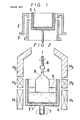
- FIG. 1 shows a schematical sectional view of the LEC apparatus of the double heater type.
- a crucible 1 is supported by a susceptor 2, around which two heaters 3 are installed.
- the two heaters 3 can be displaced upwardly and downwardly independently. Temperature distribution is changed by moving the crucible 1 with the susceptor 2 and the two independent heaters 3 upwardly or downwardly.
- the crystal pulled up from a compound melt is cooled rapidly with non-uniform temperature distribution at a cooling zone above the crystal-growing region.
- the rapid and non-uniform cooling causes the following disadvantages.
- the single crystal when pulled up is cooled rapidly and irregularly by convection of a highly pressurised gas at the cooling zone above the crucible. Strong thermal stress is generated in the crystal by the non-uniform distribution of temperature.
- the grown crystal is fragile and vulnerable.
- the crystal is apt to crack during cooling, or when the cooled crystal ingot is sliced into thin wafers then both ingot and wafers are also apt to crack.
- an LEC method for growing a single crystal of a GaAs semiconductor compound which comprises heating the compound melt in a crucible primarily utilizing a first melt heater to establish a first temperature gradient in the melt zone; heating a liquid encapsulant in the crucible primarily utilizing a crystal-growing region-controlling heater to establish a second temperature gradient in the crystal-growing region; dipping a seed crystal into the melt compound covered by molten liquid encapsulant, growing a crystal from the compound melt by pulling up and rotating the seed crystal and cooling the crystal in a cooling zone above the crucible; characterised by a cooling zone temperature-controlling means selected from a third heater and a cooling zone heat shield primarily to control the thermal environment in the uppermost portion of, and above the crucible, and further characterised by a temperature gradient in the cooling zone of 0° to 20°C/cm and which is smaller than the second temperature gradient in the crystal-growing region, which in turn is smaller than the first temperature gradient in the melt zone, whereby the
- the method of this invention has three temperature controlling means.
- the three temperature controlling means are a heater for heating the melt, a heater for controlling the thermal environment of the crystal-growing region and a heater of a heat-shield for controlling the thermal environment of the cooling zone.
- the third temperature control means seeks to provide a substantially uniform (uniform or quasi-uniform) temperature distribution in the cooling zone.
- the grown crystal is slowly cooled in a controlled manner, with a uniform or quasi-uniform temperature distribution.
- the most important matter is to control the thermal environment of the cooling zone by an independent heater or heat-shield and to cool the crystal in a uniform or quasi-uniform way.
- a big heat-shield can be installed in an outer space above the crucible, or a small heat-shield with a cylindrical shape can be floated in compound melt or liquid encapsulant.
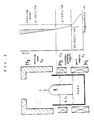
- a crucible (1) contains a compound melt (4) and a liquid encapsulant (5).
- a susceptor (2) sustains the crucible (1) on the bottom and side surfaces.
- An upper shaft (6) is installed along an axial line from the top of the chamber (not shown) enclosing everything shown in Fig. 2.
- the upper shaft (6) can rotate and move up and down.
- the seed crystal (9) is attached to the bottom end of the upper shaft (6).
- the seed crystal (9) is dipped in the compound melt (4) by lowering the upper shaft (6). Then the upper shaft (6) rotates and slowly goes upward.
- a single crystal (8) is grown in succession from the seed crystal (9).
- the lower shaft (7) supports the susceptor (2).
- the lower shaft (7) can rotate and move up and down.
- (H1) is the heater for heating compound melt. Heater (H1) heats the crucible (1) and the compound melt (4).
- the heater (H2) is the heater for heating liquid-solid interface, liquid encapsulant and single crystal in the area immediately adjacent the liquid encapsulant. This vicinity corresponds to the crystal-growing region.
- the thermal environment of the crystal-growing region can be determined by controlling the power of the heater (H2).
- the heater (H2) is designated as the crystal-growing region-controlling heater.
- (H3) is a heater for controlling the thermal environment of the space further above the liquid encapsulant (5) and the space above the crucible.
- the desirable thermal environment of these spaces is either a uniform distribution of temperature or quasi-uniform distribution of temperature with a small temperature gradient. These spaces define a zone in which the pulled single crystal is cooled. Then (H3) is designated as cooling-zone-temperature-controlling heater.
- All the heaters are resistance heaters which generate Joule heat in proportion to current and voltage.
- the melt-heating heater (H1) and the crystal-growing region-controlling heater (H2) cooperate to determine the temperature of compound melt and the thermal environment of the crystal-growing region.
- B 2 0 3 is the liquid encapsulant.
- Fig. 3 shows the distribution of temperature along a vertical center axis.
- the cooling-zone-temperature-controlling heater determines the thermal environment in which the single crystal is cooled after the crystal growth is ended.
- the cooling zone should be a zone having a uniform distribution of temperature or a zone having a quasi-uniform distribution with a small temperature gradient.
- Such a preferable thermal environment is realized mainly by controlling the cooling-zone-temperature-controlling heater (H3).
- the crystal-growing-region-controlling heater (H2) also has some influence upon the determination of the thermal environment of the cooling zone.
- Fig. 3 shows the temperature distributions.
- the area held between two lines and marked with slant parallel lines denotes an allowable temperature range distribution for the cooling zone.
- the crystal-growing-region-controlling heater (H2) mainly determines the thermal environment of liquid-solid interface, liquid encapsulant, and the space in the crucible above the liquid encapsulant.
- practical range of temperature at the cooling zone should be adjusted to be 700°C to 1000°C, preferably 850°C.
- the temperature gradient along a vertical direction at the cooling zone must be 0 to 20°C/cm.
- a single crystal pulled up to the cooling zone is cooled slowly, keeping the temperature gradient abovementioned.
- Fig. 4(A), (B) and (C) show examples of the sectional shape of cooling-zone-temperature-controlling-heater.
- Fig. (A) shows a heater of a simple cylindrical shape. Both inner diameter and outer diameter are uniform along an axial direction.
- Fig. (B) shows another heater of a transformed cylindrical shape having a conical top wall which inclines inwards.
- Fig. (C) shows another heater of a transformed cylindrical shape having a flat top wall which projects inward at a right angle with the cylinder wall.
- Heaters having the shape (B) or (C) are more preferable to form a wide zone of uniform tem- peratue than the heater having the shape (A).
- H3 has been designated a heater for controlling the thermal environment of the cooling zone.
- H3 is able to be replaced by a heat-shield with a cylindrical shape.
- a heat-shield does not heat in itself, it is sufficiently heated by the heat radiation from the other heaters (H1) and (H2) so that it can heat the cooling zone by radiating the heat obtained from (H1) and (H2). Further the heat-shield effectively suppresses convection of inert gas at the cooling zone.
- a heat-shield can replace heater (H3) and can keep the thermal environment of the cooling zone as uniform or quasi-uniform as the heater (H3).
- cooling-zone-heat-shield H3
- cooling-zone-heat-shield (H3) is not a heater, it is unable to control the thermal environment of the cooling zone directly. But the cooling-zone-heat-shield (H3) contributes to controlling the thermal environment of the cooling zone in an indirect manner by varying the powers of the heaters (H1) and (H2).
- Fig. 4(A), (B) and (C) are also fully applicable to heat-shield (H3).
- Suitable materials for the heat-shield are carbon coated with BN, carbon, carbon felt, Si0 2 , AI 2 0 3 , BN, Si 3 N 4 and PBN. Because of the high heat conductivity, carbon is the most preferable material for the heat-shield; particularly to make a uniform temperature distribution.
- the cooling-zone-heat-shield (H3) just described is fixed above the heater (H2) and has a diameter which is nearly equal to that of the crystal-growing-region-controlling-heater (H2).
- Smaller heat-shields of a cylindrical shape are also applicable to a cooling-zone-heat-shield (H3).
- the smaller heat-shield is placed in a crucible (1) in order to enclose a single crystal (8).
- Fig. 7 shows an embodiment using a small cylinder as cooling-zone heat-shield.
- the heat-shield floats in a compound melt (4) and a liquid encapsulant (5).
- the bottom of the heat-shield must not touch the bottom of the crucible (1) so as not to prevent the circulation of the compound melt.
- the smaller heat-shield (H3) is designated floating cylinder (11).
- the floating cylinder (11) may have a cylindrical sectional shape, the top portion of which inclines inwardly.
- This shape effectively suppresses inert gas circulation between the inner space and the outer space of the floating cylinder (11) and reduces heat dissipation by convection.
- the material of the floating cylinder is carbon coated with BN or AIN.
- a coating protects the compound melt and the single crystal from contamination by carbon powder.
- the floating cylinder (11) must float in liquid.
- the top end of the floating cylinder must enclose the single crystal therein until crystal growth has preceeded to a considerable extent.
- a floating cylinder (11) with a cavity shown in Fig. 8 is to be preferred.
- Floating cylinders can have various shapes-a cylinder with step part on the inner wall, a cylinder having a widening conical upper wall with a bigger top opening, or a cylinder having a narrowing conical upper wall with a smaller top opening.
- the shape and the size of the floating cylinder are determined to adjust it to a desired thermal environment and the conditions for pulling up a crystal.
- the crucible's height H is 150 mm
- the inner diameter D is 150 mm
- the floating cylinder's inner diameter d is 102 mm
- the outer diameter d 2 is 149 mm.
- the distance k from the bottom end of the floating cylinder to the liquid-solid interface is 5 mm.
- the method of the invention allows a GaAs single crystal to be pulled up through the crystal-growing-region with small temperature gradient. And the grown crystal is slowly cooled in the cooling zone having a uniform or quasi-uniform distribution of temperature.
- GaAs crystal production according to the invention is now described by way of illustration only.
- a GaAs crystal is pulled up by the LEC apparatus shown in Fig. 2.
- H3 is a heater
- the melt-heating heater (H1), the crystal-growing-region-controlling heater (H2) and the cooling-zone-temperature controlling heater (H3) are turned on and the temperatures of the heaters rise to the prescribed values.
- GaAs compound melt 4 Kg is generated in the crucible.
- the compound melt is covered with a liquid encapsulant.
- Two atm to fifty atm (2x10 5 to 5x10 6 Pa) of nitrogen gas fills the chamber (not shown in figures).
- the necessary gas pressure depends on the thickness of B 2 0 3 layer.
- B 2 0 3 layer is thick, even three atm (3x10 5 Pa) of nitrogen gas is sufficient to press the B 2 0 3 layer.
- optimum range of gas pressure is 15 to 20 atm (15x10 5 to 2x10 6 Pa).
- the process for raising temperature in the case wherein starting material is polycrystalline GaAs differs from the process in the case wherein GaAs compound is directly synthesized from pure Ga and pure As.
- the melt-heating heater (H1), the crystal-growing-region-controlling heater (H2) and the cooling-zone-temperature-controlling heater (H3) are turned on the same time.
- the temperatures of the three heaters rise in proportion to each other.
- Raising the temperature of the cooling-zone-temperature-controlling heater (H3) is stopped when the temperature at a measuring point on the outer surface of the heater (H3) attains 870°C.
- the temperature at a measuring point on the outer surface of the melt-heating heater (H1) is about 1200°C
- the temperature at a measuring point on the outer surface of the crystal-growing-region-controlling heater (H2) is about 1000°C.
- the melt-heating heater (H1) is still kept turned on.
- the heating of the heater (H1) is stopped.
- the temperature of the crystal-growing-region-controlling-heater (H2) is adjusted to be 900°C to 1100°C at the time.
- GaAs compound is directly synthesized from Ga and As in the crucible.
- GaAs compound is synthesized by the chemical reaction in a direct manner.
- Seeding is done about 30 minutes after the compound melt of GaAs is generated. A seed crystal is dipped into the compound melt.
- the conditions of the crystal growth are,
- the crystal is still pulled upward into the cooling zone and is stopped there as shown in Fig. 5.
- the crystal is slowly cooled in a uniform or quasi-uniform temperature distribution which is kept by adjusting the electric power of the heaters (H1), (H2) and (H3).
- the crystal cooled to room temperature is then detached from the LEC apparatus.
- the crystal is (7,56 cm) 3 inches, in diameter.
- the weight of the crystal is 3820 g, and the length is 19 cm. This crystal is a single crystal without cracks.
- a GaAs single crystal of high quality is thus obtained.
- the single crystal is sliced into wafers and the distributions of etch pit density (EPD) in wafers are measured.
- EPD etch pit density
- Fig. 6(A) is a diagram showing the distributions of measured etch pit density on two wafers sliced from the head and tail portions of the crystal.
- the Abscissa denotes the distances from the center of wafer.
- the Ordinate denotes EPD in a logarithmic scale.
- Both distributions of EPD on the tail wafer and the head wafer are lower than 3x10 4 cm- 2 .
- Fig. 6(B) is a diagram showing the distributions of measured etch pit densities on two wafers sliced from the head and tail portions of a GaAs single crystal grown by a conventional LEC method and apparatus having only a single heater.
- the distributions of EPD is about 10 5 cm- 2 .
- the following steps are subsequently effected on the crystal; grinding of the outer surface to adjust the diameter to within a prescribed value, and marking of orientation flats which denote the crystallographical axes.
- the crystals made by this invention do not crack during these steps.
- the yield after grinding the outer surface to adjust the diameter to the allowable range of from 7.56 cm plus or minus 1 mm and marking orientation flats was about 33% in a conventional LEC method. But the same yield rises to 60%, with this invention.
- EPD decreases to nearly one tenth of the aforementioned embodiment by doping more than 10 19 /cm' of In or Sb into the crystal.
Landscapes
- Chemical & Material Sciences (AREA)
- Engineering & Computer Science (AREA)
- Crystallography & Structural Chemistry (AREA)
- Materials Engineering (AREA)
- Metallurgy (AREA)
- Organic Chemistry (AREA)
- Crystals, And After-Treatments Of Crystals (AREA)
- Liquid Deposition Of Substances Of Which Semiconductor Devices Are Composed (AREA)
Claims (2)
Applications Claiming Priority (2)
| Application Number | Priority Date | Filing Date | Title |
|---|---|---|---|
| JP58154771A JPS6046998A (ja) | 1983-08-26 | 1983-08-26 | 単結晶引上方法及びそのための装置 |
| JP154771/83 | 1983-08-26 |
Publications (2)
| Publication Number | Publication Date |
|---|---|
| EP0140509A1 EP0140509A1 (fr) | 1985-05-08 |
| EP0140509B1 true EP0140509B1 (fr) | 1988-10-26 |
Family
ID=15591532
Family Applications (1)
| Application Number | Title | Priority Date | Filing Date |
|---|---|---|---|
| EP84305606A Expired EP0140509B1 (fr) | 1983-08-26 | 1984-08-17 | Méthode LEC et appareil pour la croissance d'un mono-cristal d'un composé semi-conducteur |
Country Status (4)
| Country | Link |
|---|---|
| US (1) | US4645560A (fr) |
| EP (1) | EP0140509B1 (fr) |
| JP (1) | JPS6046998A (fr) |
| DE (1) | DE3474842D1 (fr) |
Cited By (1)
| Publication number | Priority date | Publication date | Assignee | Title |
|---|---|---|---|---|
| DE4030551A1 (de) * | 1989-09-29 | 1991-04-11 | Osaka Titanium | Verfahren zur herstellung von silicium-einkristallen |
Families Citing this family (25)
| Publication number | Priority date | Publication date | Assignee | Title |
|---|---|---|---|---|
| JP2553485B2 (ja) * | 1983-11-30 | 1996-11-13 | 住友電気工業株式会社 | 砒化ガリウム単結晶の製造方法 |
| JP2529934B2 (ja) * | 1984-02-21 | 1996-09-04 | 住友電気工業株式会社 | 単結晶の製造方法 |
| US5770873A (en) | 1984-10-05 | 1998-06-23 | Hitachi, Ltd. | GaAs single crystal as well as method of producing the same, and semiconductor device utilizing the GaAs single crystal |
| IT1207497B (it) * | 1985-05-29 | 1989-05-25 | Montedison Spa | Monocristalli di arseniuro di gallio a bassa densita' di dislocazioni e di elevata purezza. |
| US4740264A (en) * | 1986-10-29 | 1988-04-26 | The United States Of America As Represented By The Administrator Of The National Aeronautics And Space Administration | Liquid encapsulated float zone process and apparatus |
| US4738831A (en) * | 1986-10-31 | 1988-04-19 | The United States Of America As Represented By The Administrator Of The National Aeronautics & Space Administration | Method and apparatus for growing crystals |
| JP2757865B2 (ja) * | 1987-03-23 | 1998-05-25 | 住友電気工業株式会社 | ▲iii▼−▲v▼族化合物半導体単結晶の製造方法 |
| US4822449A (en) * | 1987-06-10 | 1989-04-18 | Massachusetts Institute Of Technology | Heat transfer control during crystal growth |
| FR2617870B1 (fr) * | 1987-07-09 | 1989-10-27 | Labo Electronique Physique | Procede de realisation de plaquettes-substrats orientees, a partir de lingots massifs semi-conducteurs du groupe iii-v |
| JP2645491B2 (ja) * | 1987-09-07 | 1997-08-25 | 株式会社ジャパンエナジー | 化合物半導体単結晶の育成方法 |
| JPH0259489A (ja) * | 1988-08-25 | 1990-02-28 | Shin Etsu Handotai Co Ltd | 化合物半導体単結晶の製造方法 |
| JPH0261965U (fr) * | 1988-10-27 | 1990-05-09 | ||
| US5078830A (en) * | 1989-04-10 | 1992-01-07 | Mitsubishi Metal Corporation | Method for growing single crystal |
| US5154795A (en) * | 1989-06-12 | 1992-10-13 | Mitsubishi Kasei Polytec Company | System for setting analysis condition for a thermal analysis of a fluid inside an apparatus |
| US5114528A (en) * | 1990-08-07 | 1992-05-19 | Wisconsin Alumni Research Foundation | Edge-defined contact heater apparatus and method for floating zone crystal growth |
| JP2640315B2 (ja) * | 1993-03-22 | 1997-08-13 | 住友シチックス株式会社 | シリコン単結晶の製造方法 |
| JP3128795B2 (ja) * | 1995-06-09 | 2001-01-29 | 信越半導体株式会社 | チョクラルスキー法による結晶製造装置および製造方法 |
| JP3531333B2 (ja) * | 1996-02-14 | 2004-05-31 | 信越半導体株式会社 | チョクラルスキー法による結晶製造装置、結晶製造方法、およびこの方法から製造される結晶 |
| US6379642B1 (en) * | 1997-04-09 | 2002-04-30 | Memc Electronic Materials, Inc. | Vacancy dominated, defect-free silicon |
| US6809027B2 (en) * | 2002-06-06 | 2004-10-26 | International Business Machines Corporation | Self-aligned borderless contacts |
| RU2261296C1 (ru) * | 2004-08-05 | 2005-09-27 | Амосов Владимир Ильич | Устройство для выращивания монокристаллов из расплава |
| RU2261297C1 (ru) * | 2004-08-05 | 2005-09-27 | Амосов Владимир Ильич | Способ выращивания монокристаллов из расплава методом амосова |
| KR101391057B1 (ko) * | 2005-09-30 | 2014-04-30 | 사무코 테크시부 가부시키가이샤 | 단결정 반도체 제조 장치 및 제조 방법 |
| KR101263082B1 (ko) * | 2010-11-15 | 2013-05-09 | 주식회사 엘지실트론 | 사파이어 잉곳 성장장치 |
| JP6300786B2 (ja) * | 2013-03-26 | 2018-04-04 | Jx金属株式会社 | リン化インジウム単結晶の製造方法 |
Family Cites Families (13)
| Publication number | Priority date | Publication date | Assignee | Title |
|---|---|---|---|---|
| DE132704C (fr) * | ||||
| FR1522416A (fr) * | 1967-03-14 | 1968-04-26 | Comp Generale Electricite | Perfectionnements au procédé d'obtention de cristaux par tirage |
| JPS4949307B1 (fr) * | 1970-02-18 | 1974-12-26 | ||
| US4140570A (en) * | 1973-11-19 | 1979-02-20 | Texas Instruments Incorporated | Method of growing single crystal silicon by the Czochralski method which eliminates the need for post growth annealing for resistivity stabilization |
| DE2542090C2 (de) * | 1975-09-20 | 1983-08-25 | Bayer Ag, 5090 Leverkusen | Kondensationsprodukte aus Cycloalkanonen, Formaldehyd und Alkalibisulfit |
| JPS5912632B2 (ja) * | 1975-11-22 | 1984-03-24 | 住友電気工業株式会社 | タンケツシヨウノヒキアゲソウチ |
| US4314128A (en) * | 1980-01-28 | 1982-02-02 | Photowatt International, Inc. | Silicon growth technique and apparatus using controlled microwave heating |
| JPS5711897A (en) * | 1980-06-27 | 1982-01-21 | Sumitomo Electric Ind Ltd | Method of pulling up single crystal and device therefor |
| JPS57179095A (en) * | 1981-04-28 | 1982-11-04 | Tohoku Metal Ind Ltd | Method and apparatus for manufacturing single crystal |
| JPS58135626A (ja) * | 1982-02-08 | 1983-08-12 | Nippon Telegr & Teleph Corp <Ntt> | 化合物半導体単結晶の製造方法及び製造装置 |
| JPS5957986A (ja) * | 1982-09-24 | 1984-04-03 | Sumitomo Electric Ind Ltd | 単結晶引上方法 |
| JPS5964591A (ja) * | 1982-09-30 | 1984-04-12 | Sumitomo Electric Ind Ltd | 単結晶引上装置 |
| JPH0669917B2 (ja) * | 1982-10-08 | 1994-09-07 | 住友電気工業株式会社 | 複数段ヒ−タ−の制御方法 |
-
1983
- 1983-08-26 JP JP58154771A patent/JPS6046998A/ja active Granted
-
1984
- 1984-08-17 DE DE8484305606T patent/DE3474842D1/de not_active Expired
- 1984-08-17 EP EP84305606A patent/EP0140509B1/fr not_active Expired
- 1984-08-24 US US06/644,009 patent/US4645560A/en not_active Expired - Lifetime
Cited By (2)
| Publication number | Priority date | Publication date | Assignee | Title |
|---|---|---|---|---|
| DE4030551A1 (de) * | 1989-09-29 | 1991-04-11 | Osaka Titanium | Verfahren zur herstellung von silicium-einkristallen |
| DE4030551C2 (fr) * | 1989-09-29 | 1992-12-17 | Osaka Titanium Co. Ltd., Amagasaki, Hyogo, Jp |
Also Published As
| Publication number | Publication date |
|---|---|
| DE3474842D1 (en) | 1988-12-01 |
| EP0140509A1 (fr) | 1985-05-08 |
| JPH0328398B2 (fr) | 1991-04-18 |
| US4645560A (en) | 1987-02-24 |
| JPS6046998A (ja) | 1985-03-14 |
Similar Documents
| Publication | Publication Date | Title |
|---|---|---|
| EP0140509B1 (fr) | Méthode LEC et appareil pour la croissance d'un mono-cristal d'un composé semi-conducteur | |
| CA2452542C (fr) | Procede et appareil servant a la croissance de cristaux semi-conducteurs au moyen d'un support rigide, dopage au carbone, d'une regulation de la resistivite et du gradient de temperature | |
| EP0068021B1 (fr) | Procede et appareil de formation et de developpement d'un monocristal d'un compose semi-conducteur | |
| KR100687511B1 (ko) | 결정 인상기용 열차단 어셈블리 | |
| US5429067A (en) | Czochralski method using a member for intercepting radiation from a raw material molten solution | |
| US3798007A (en) | Method and apparatus for producing large diameter monocrystals | |
| US5714004A (en) | Process for producing polycrystalline semiconductors | |
| US20120282133A1 (en) | Crystal growth apparatus and method | |
| CA1336061C (fr) | Substrat de monocristal de silicium a haute teneur en oxygene pour systemes de semi-conducteurs; methode de preparation | |
| US5047113A (en) | Method for directional solidification of single crystals | |
| US4840699A (en) | Gallium arsenide crystal growth | |
| JP3533812B2 (ja) | チョクラルスキー法による結晶製造装置、結晶製造方法、およびこの方法から製造される結晶 | |
| KR100331552B1 (ko) | 잉곳-용융물 경계의 중앙 및 가장자리에서의 온도구배의 조절에 의한 단결정 실리콘 잉곳의 제조를 위한 초크랄스키 풀러, 상기 초크랄스키 풀러용 열차단체 및 상기 초크랄스키 풀러의 개량방법. | |
| EP0210439B1 (fr) | Méthode de croissance de monocristaux d'un composé semi-conducteur dissociable | |
| EP2501844A1 (fr) | Appareil et procédé de croissance des cristaux | |
| JP3079991B2 (ja) | 単結晶の製造装置および製造方法 | |
| JP2010030847A (ja) | 半導体単結晶の製造方法 | |
| JPH03193689A (ja) | 化合物半導体の結晶製造方法 | |
| JPH0782084A (ja) | 単結晶成長方法及び単結晶成長装置 | |
| JPH05319973A (ja) | 単結晶製造装置 | |
| JPS60122791A (ja) | 液体封止結晶引上方法 | |
| JP2005132717A (ja) | 化合物半導体単結晶およびその製造方法 | |
| JP2000169278A (ja) | 半導体結晶の製造方法および製造装置 | |
| JPH07206589A (ja) | 化合物半導体単結晶の製造方法 | |
| JPH08259371A (ja) | Srの均一化に優れる単結晶成長方法 |
Legal Events
| Date | Code | Title | Description |
|---|---|---|---|
| PUAI | Public reference made under article 153(3) epc to a published international application that has entered the european phase |
Free format text: ORIGINAL CODE: 0009012 |
|
| AK | Designated contracting states |
Designated state(s): DE FR GB |
|
| 17P | Request for examination filed |
Effective date: 19850419 |
|
| RAP1 | Party data changed (applicant data changed or rights of an application transferred) |
Owner name: NIPPON TELEGRAPH AND TELEPHONE CORPORATION Owner name: SUMITOMO ELECTRIC INDUSTRIES LIMITED |
|
| 17Q | First examination report despatched |
Effective date: 19860124 |
|
| GRAA | (expected) grant |
Free format text: ORIGINAL CODE: 0009210 |
|
| AK | Designated contracting states |
Kind code of ref document: B1 Designated state(s): DE FR GB |
|
| REF | Corresponds to: |
Ref document number: 3474842 Country of ref document: DE Date of ref document: 19881201 |
|
| ET | Fr: translation filed | ||
| PLBE | No opposition filed within time limit |
Free format text: ORIGINAL CODE: 0009261 |
|
| STAA | Information on the status of an ep patent application or granted ep patent |
Free format text: STATUS: NO OPPOSITION FILED WITHIN TIME LIMIT |
|
| 26N | No opposition filed | ||
| REG | Reference to a national code |
Ref country code: GB Ref legal event code: IF02 |
|
| PGFP | Annual fee paid to national office [announced via postgrant information from national office to epo] |
Ref country code: FR Payment date: 20030808 Year of fee payment: 20 |
|
| PGFP | Annual fee paid to national office [announced via postgrant information from national office to epo] |
Ref country code: GB Payment date: 20030813 Year of fee payment: 20 |
|
| PGFP | Annual fee paid to national office [announced via postgrant information from national office to epo] |
Ref country code: DE Payment date: 20030828 Year of fee payment: 20 |
|
| PG25 | Lapsed in a contracting state [announced via postgrant information from national office to epo] |
Ref country code: GB Free format text: LAPSE BECAUSE OF EXPIRATION OF PROTECTION Effective date: 20040816 |
|
| REG | Reference to a national code |
Ref country code: GB Ref legal event code: PE20 |