EP0108480A2 - Photoelektrisches Umsetzungselement - Google Patents
Photoelektrisches Umsetzungselement Download PDFInfo
- Publication number
- EP0108480A2 EP0108480A2 EP83305333A EP83305333A EP0108480A2 EP 0108480 A2 EP0108480 A2 EP 0108480A2 EP 83305333 A EP83305333 A EP 83305333A EP 83305333 A EP83305333 A EP 83305333A EP 0108480 A2 EP0108480 A2 EP 0108480A2
- Authority
- EP
- European Patent Office
- Prior art keywords
- photoelectric conversion
- separate electrodes
- light shielding
- transparent electrode
- conductive layer
- Prior art date
- Legal status (The legal status is an assumption and is not a legal conclusion. Google has not performed a legal analysis and makes no representation as to the accuracy of the status listed.)
- Granted
Links
- 238000006243 chemical reaction Methods 0.000 title claims abstract description 66
- 239000000758 substrate Substances 0.000 claims abstract description 19
- 239000000463 material Substances 0.000 claims description 7
- 229920005989 resin Polymers 0.000 claims description 7
- 239000011347 resin Substances 0.000 claims description 7
- 229910052804 chromium Inorganic materials 0.000 claims description 5
- 229910052738 indium Inorganic materials 0.000 claims description 3
- 229910052719 titanium Inorganic materials 0.000 claims description 3
- 229910052721 tungsten Inorganic materials 0.000 claims description 3
- 229910052720 vanadium Inorganic materials 0.000 claims description 3
- 229910052789 astatine Inorganic materials 0.000 claims description 2
- 229910052802 copper Inorganic materials 0.000 claims description 2
- 239000003822 epoxy resin Substances 0.000 claims description 2
- 229910052745 lead Inorganic materials 0.000 claims description 2
- 229910052748 manganese Inorganic materials 0.000 claims description 2
- 229910052759 nickel Inorganic materials 0.000 claims description 2
- 229910052763 palladium Inorganic materials 0.000 claims description 2
- 229910052697 platinum Inorganic materials 0.000 claims description 2
- 229920000647 polyepoxide Polymers 0.000 claims description 2
- 229910052709 silver Inorganic materials 0.000 claims description 2
- 239000010410 layer Substances 0.000 description 39
- 239000010408 film Substances 0.000 description 14
- 238000010276 construction Methods 0.000 description 5
- 239000011651 chromium Substances 0.000 description 4
- 238000005530 etching Methods 0.000 description 4
- 239000011521 glass Substances 0.000 description 4
- 238000004544 sputter deposition Methods 0.000 description 4
- HEMHJVSKTPXQMS-UHFFFAOYSA-M Sodium hydroxide Chemical compound [OH-].[Na+] HEMHJVSKTPXQMS-UHFFFAOYSA-M 0.000 description 3
- 239000002253 acid Substances 0.000 description 3
- 229910052782 aluminium Inorganic materials 0.000 description 3
- XAGFODPZIPBFFR-UHFFFAOYSA-N aluminium Chemical compound [Al] XAGFODPZIPBFFR-UHFFFAOYSA-N 0.000 description 3
- 229910021417 amorphous silicon Inorganic materials 0.000 description 3
- 239000011241 protective layer Substances 0.000 description 3
- VYZAMTAEIAYCRO-UHFFFAOYSA-N Chromium Chemical compound [Cr] VYZAMTAEIAYCRO-UHFFFAOYSA-N 0.000 description 2
- OAICVXFJPJFONN-UHFFFAOYSA-N Phosphorus Chemical compound [P] OAICVXFJPJFONN-UHFFFAOYSA-N 0.000 description 2
- 239000000919 ceramic Substances 0.000 description 2
- 230000006866 deterioration Effects 0.000 description 2
- 239000007788 liquid Substances 0.000 description 2
- 229910052751 metal Inorganic materials 0.000 description 2
- 239000002184 metal Substances 0.000 description 2
- 238000000059 patterning Methods 0.000 description 2
- 229920001296 polysiloxane Polymers 0.000 description 2
- 239000010936 titanium Substances 0.000 description 2
- 239000004593 Epoxy Substances 0.000 description 1
- JOYRKODLDBILNP-UHFFFAOYSA-N Ethyl urethane Chemical compound CCOC(N)=O JOYRKODLDBILNP-UHFFFAOYSA-N 0.000 description 1
- KJTLSVCANCCWHF-UHFFFAOYSA-N Ruthenium Chemical compound [Ru] KJTLSVCANCCWHF-UHFFFAOYSA-N 0.000 description 1
- GWEVSGVZZGPLCZ-UHFFFAOYSA-N Titan oxide Chemical compound O=[Ti]=O GWEVSGVZZGPLCZ-UHFFFAOYSA-N 0.000 description 1
- NIXOWILDQLNWCW-UHFFFAOYSA-N acrylic acid group Chemical group C(C=C)(=O)O NIXOWILDQLNWCW-UHFFFAOYSA-N 0.000 description 1
- 239000002390 adhesive tape Substances 0.000 description 1
- 239000003513 alkali Substances 0.000 description 1
- PNEYBMLMFCGWSK-UHFFFAOYSA-N aluminium oxide Inorganic materials [O-2].[O-2].[O-2].[Al+3].[Al+3] PNEYBMLMFCGWSK-UHFFFAOYSA-N 0.000 description 1
- 239000007864 aqueous solution Substances 0.000 description 1
- 239000011248 coating agent Substances 0.000 description 1
- 238000000576 coating method Methods 0.000 description 1
- 239000010949 copper Substances 0.000 description 1
- 229910052593 corundum Inorganic materials 0.000 description 1
- 230000005611 electricity Effects 0.000 description 1
- 230000008020 evaporation Effects 0.000 description 1
- 238000001704 evaporation Methods 0.000 description 1
- 229910052732 germanium Inorganic materials 0.000 description 1
- GNPVGFCGXDBREM-UHFFFAOYSA-N germanium atom Chemical compound [Ge] GNPVGFCGXDBREM-UHFFFAOYSA-N 0.000 description 1
- PCHJSUWPFVWCPO-UHFFFAOYSA-N gold Chemical compound [Au] PCHJSUWPFVWCPO-UHFFFAOYSA-N 0.000 description 1
- 229910052737 gold Inorganic materials 0.000 description 1
- 239000010931 gold Substances 0.000 description 1
- 238000010438 heat treatment Methods 0.000 description 1
- AMGQUBHHOARCQH-UHFFFAOYSA-N indium;oxotin Chemical compound [In].[Sn]=O AMGQUBHHOARCQH-UHFFFAOYSA-N 0.000 description 1
- 229910010272 inorganic material Inorganic materials 0.000 description 1
- 239000011147 inorganic material Substances 0.000 description 1
- 239000011810 insulating material Substances 0.000 description 1
- 239000011572 manganese Substances 0.000 description 1
- 238000004519 manufacturing process Methods 0.000 description 1
- DZVCFNFOPIZQKX-LTHRDKTGSA-M merocyanine Chemical compound [Na+].O=C1N(CCCC)C(=O)N(CCCC)C(=O)C1=C\C=C\C=C/1N(CCCS([O-])(=O)=O)C2=CC=CC=C2O\1 DZVCFNFOPIZQKX-LTHRDKTGSA-M 0.000 description 1
- 150000002739 metals Chemical class 0.000 description 1
- 238000000034 method Methods 0.000 description 1
- 239000000203 mixture Substances 0.000 description 1
- PXHVJJICTQNCMI-UHFFFAOYSA-N nickel Substances [Ni] PXHVJJICTQNCMI-UHFFFAOYSA-N 0.000 description 1
- 230000003287 optical effect Effects 0.000 description 1
- 238000004806 packaging method and process Methods 0.000 description 1
- FIKAKWIAUPDISJ-UHFFFAOYSA-L paraquat dichloride Chemical compound [Cl-].[Cl-].C1=C[N+](C)=CC=C1C1=CC=[N+](C)C=C1 FIKAKWIAUPDISJ-UHFFFAOYSA-L 0.000 description 1
- IEQIEDJGQAUEQZ-UHFFFAOYSA-N phthalocyanine Chemical compound N1C(N=C2C3=CC=CC=C3C(N=C3C4=CC=CC=C4C(=N4)N3)=N2)=C(C=CC=C2)C2=C1N=C1C2=CC=CC=C2C4=N1 IEQIEDJGQAUEQZ-UHFFFAOYSA-N 0.000 description 1
- 238000005268 plasma chemical vapour deposition Methods 0.000 description 1
- 229910021420 polycrystalline silicon Inorganic materials 0.000 description 1
- 150000004032 porphyrins Chemical class 0.000 description 1
- 238000009877 rendering Methods 0.000 description 1
- 229910052707 ruthenium Inorganic materials 0.000 description 1
- 238000005507 spraying Methods 0.000 description 1
- 239000010409 thin film Substances 0.000 description 1
- OGIDPMRJRNCKJF-UHFFFAOYSA-N titanium oxide Inorganic materials [Ti]=O OGIDPMRJRNCKJF-UHFFFAOYSA-N 0.000 description 1
- 229910001845 yogo sapphire Inorganic materials 0.000 description 1
Images


Classifications
-
- H—ELECTRICITY
- H10—SEMICONDUCTOR DEVICES; ELECTRIC SOLID-STATE DEVICES NOT OTHERWISE PROVIDED FOR
- H10F—INORGANIC SEMICONDUCTOR DEVICES SENSITIVE TO INFRARED RADIATION, LIGHT, ELECTROMAGNETIC RADIATION OF SHORTER WAVELENGTH OR CORPUSCULAR RADIATION
- H10F39/00—Integrated devices, or assemblies of multiple devices, comprising at least one element covered by group H10F30/00, e.g. radiation detectors comprising photodiode arrays
- H10F39/10—Integrated devices
- H10F39/12—Image sensors
- H10F39/191—Photoconductor image sensors
-
- H—ELECTRICITY
- H10—SEMICONDUCTOR DEVICES; ELECTRIC SOLID-STATE DEVICES NOT OTHERWISE PROVIDED FOR
- H10F—INORGANIC SEMICONDUCTOR DEVICES SENSITIVE TO INFRARED RADIATION, LIGHT, ELECTROMAGNETIC RADIATION OF SHORTER WAVELENGTH OR CORPUSCULAR RADIATION
- H10F39/00—Integrated devices, or assemblies of multiple devices, comprising at least one element covered by group H10F30/00, e.g. radiation detectors comprising photodiode arrays
- H10F39/80—Constructional details of image sensors
- H10F39/802—Geometry or disposition of elements in pixels, e.g. address-lines or gate electrodes
-
- H—ELECTRICITY
- H10—SEMICONDUCTOR DEVICES; ELECTRIC SOLID-STATE DEVICES NOT OTHERWISE PROVIDED FOR
- H10F—INORGANIC SEMICONDUCTOR DEVICES SENSITIVE TO INFRARED RADIATION, LIGHT, ELECTROMAGNETIC RADIATION OF SHORTER WAVELENGTH OR CORPUSCULAR RADIATION
- H10F39/00—Integrated devices, or assemblies of multiple devices, comprising at least one element covered by group H10F30/00, e.g. radiation detectors comprising photodiode arrays
- H10F39/80—Constructional details of image sensors
- H10F39/805—Coatings
- H10F39/8057—Optical shielding
Definitions
- the present invention relates to a photoelectric conversion element.
- a photoelectric conversion element which serves to convert a quantity of light into a quantity of electricity such as an electric charge quantity or change of conductance, is used in an image sensing device included in, for example, facsimile or a copying machines.
- a photoelectric conversion element using a CCD (charge coupled device) is under development.
- the phosphor screen width is small in this element, with the result that it is necessary to reduce the optical information by a lens system for projection into the phosphor screen.
- the photoelectric conversion element necessitates a reduction lens system, leading to enlargement of the device. Also miniaturization of the image is restricted by the reduction requirements.
- FIG. lA is a plan view showing a part of a photoelectric conversion element
- Fig. 1B is a cross-sectional view along line A-A shown in Fig. lA.
- a plurality of separate electrodes 2 made of aluminum or chromium are arranged in a row on a glass substrate 1. These separate electrodes 2 are covered with a photoelectric conversion layer 3. Further, the photoelectric layer 3 is covered with a transparent electrode 4. Since the transparent electrode 4 has low electric conductivity, an auxiliary electrode 5 is generally provided.
- the overlapped portion of the separate electrodes 2, photoelectric conversion layer 3, and transparent electrode 4 performs the light detecting function.
- a photoelectric conversion element is designed such that the overlapped portion alone acts as a light sensing part.
- the transparent electrode 4 is formed by mask sputtering. There is about 200 ⁇ m in repeatability error of mask alignment in the mask sputtering method.
- the transparent electrode 4 is partially overlapped with the lead-out parts 2a of the separate electrodes 2. Since ,the overlapped portion also detects light, noise is generated, resulting in deterioration of resolution in the sub-scanning direction.
- An object of the present invention is to provide a photoelectric conversion element low in noise generation, free of resolution deterioration in the sub-scanning direction, and capable of reading out fine images accurately.
- a photoelectric conversion element comprising: a substrate, a plurality of separate electrodes arranged in a row on the substrate, signal lead-out parts extending from the separate electrodes alternately to the left and the right, a photoelectric conversion layer convering the row of the separate electrodes, a transparent electrode formed on the photoelectric conversion layer, and a light shielding conductive layer formed on the transparent electrode to shield the light projected toward the overlapping portion between at least those portions of the signal lead-out parts which abut against the separate electrodes and the photoelectric conversion layer.
- Insulating materials such as ceramics and glass are used as the substrate in the present invention. Since a ceramic substrate is porous, it is desirable to form a glaze layer on the surface to obtain a smooth surface.
- the separate electrodes and signal lead-out parts are made of a metal such as At, Cr, Ti, V, W, and In, and can be formed by evaporation, sputtering, or the like.
- the separate electrodes serve to detect the electric quantity converted by the photoelectric conversion layer.
- the signal lead-out parts serve to lead the signals from the separate electrodes to the outside.
- separate electrodes and signal lead-out parts are integrally formed.
- photoconductive materials which permit converting a light quantity into an electric quantity such as charge quantity or a change of conductance, can be used for forming the photoelectric conversion layer.
- the photoconductive materials mentioned include, inorganic photoconductive materials such as amorphous silicon, amorphous SiC, poly-Si and amorphous germanium; organic dyestuffs such as merocyanine, phthalocyanine, pyrrium, and'squarium; and organic photoconductive materials such as porphyrin, ruthenium trisbipyrydine complex, and a mixture of titanium oxide and methylviologen.
- Materials having electric conductivity and transmitting light such as nesa film, ITO (indium tin oxide) film and gold thin film can be used as the transparent electrode.
- the light shielding conductive layer while compensating for the conductivity of the transparent electrode, serves to shield the light projected to the overlapping portion between the signal lead-out part and the photoelectric conversion layer.
- the light shielding conductive layer is formed of metals like M, Au, Mo, Mn, Ni, Cr, Cu, Ti, V, W, Ag, Pd, Pt, In, Pb, and conductive epoxy resin, etc. These materials are deposited or coated by the ordinary method, followed by selectively etching the deposited or coated layer to form a light shielding layer of a desired form.
- the photoelectric conversion element having the construction described above it is possible to shield the light projected onto an undesirable portion, i.e., an overlapping portion among the signal lead-out part, photoelectric conversion layer, and transparent electrode, thereby making it possible to suppress the noise generated from the overlapping portion. Also, since the light shielding conductive layer performing the shielding function is capable of compensating for the conductivity of the transparent electrode, the auxiliary electrode used in the past need not be provided in the present invention.
- the auxiliary electrode need not be provided on one side of the substrate as mentioned above, it is possible to allow the signal lead-out parts to extend to the left and right in a direction perpendicular to the arranging direction of the separate electrodes. As a result, the density of the signal lead-out parts can be reduced to half the'conventional level and the density of the separate electrodes can be increased to about twice the conventional level, so that a very fine photoelectric conversion element can be made.
- the photoelectric conversion element of the present invention is suitable for use as a large image sensor which does not require a reduction lens system.
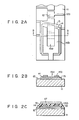
- chromium is deposited on a glass substrate 11, followed by patterning of the deposited layer to form a plurality of separate electrodes 12 arranged in a row and provided with signal lead-out parts 12a.
- the separate electrodes 12 are covered with a photoelectric conversion layer 13 consisting of amorphous silicon and formed by the plasma CVD method.
- the photoelectric conversion layer 13 is covered with a transparent electrode 14 consisting of an ITO film and formed by sputtering or spraying.
- an aluminum film is deposited on the transparent electrode 14. The aluminum film is selectively etched to remove the region above the row of separate electrodes 12, thereby forming a light shielding electrode 15b having a slit-like opening 15a.
- the light shielding electrode 15b covers that portion of the transparent electrode 14 which corresponds to the signal lead-out parts 12a abutting against the separate electrodes 12. If an acid etching liquid is used to etch the light shielding electrode 15b, the ITO film constituting the transparent electrode 14 is etched. Thus, it is necessary to use an alkali etching liquid, e.g., an aqueous solution of sodium hydroxide.
- the etching is performed by using, for example, a resist pattern as a mask.
- the mask can be aligned with high accuracy of, e.g., several microns.
- the structure shown in Figs. 2A and 2B may be coated with a moistureproof protective layer 16. Further, the moistureproof protective layer 16 may De coverea with a glass layer 17.
- the light projected onto the overlapping portion among the signal dead-cut parts 12a, photoelectric conversion element 13, and transparent electrode 14 is shielded by the light shielding conductive layer 15b to prevent noise generation from the overlapping portion.
- the signal lead-out parts 12a extend from the separate electrodes 12 alternately to the left and right in a direction perpendicular to the arranging direction of the separate electrodes 12, it is possible to reduce the density of the signal lead-out parts 12a to half the level of the conventional photoelectric conversion element. Likewise, the density of the separate electrodes can be increased to about twice the conventional level.
- the upper limit of the density of the signal lead-out parts is about 8 lead-out parts/mm in the conventional photoelectric conversion element because of the restriction in packaging.
- the upper limit of the density of the separate electrodes is also 8 electrodes/mm in the conventional element.
- the signal lead-out parts 12 are disposed on both sides of the substrate.
- the density on both sides i.e., the density on the elment, is 16 lead-out parts/mm.
- the light shielding conductive film 14 can compensate for the conductivity of the transparent electrode 14, making it possible to eliminate the auxiliary electrode provided on one side of the substrate in the conventional element.
- the transparent electrode has a resistance as high as about 10 kn.
- the resistance of the transparent electrode is less than 1/100 the value for the element which does not include a light shielding conductive film. It follows that the photoelectric conversion element of the present invention is effective for detecting fine signals. Particularly, where the element is used in the store mode, the signal read-out speed is not lowered because the resistance of the transparent electrode influences the time constant of the signal read-out.
- a contact type image sensor it is necessary to converge a light beam by, for example, a rod array lens to guide the beam to the photoelectric conversion element.
- the photoelectric conversion element of the present invention provided with a light shielding conductive layer having a slit-like opening is used in such an image sensor, the light beam projected onto the undesired portion is shielded by the light shielding conductive layer to enable the image sensor to operate quite satisfactorily.
- the signals generated from the separate electrodes are read out by turning on successively the MOS switches connected to the separate electrodes.
- the dark output during light non-irradiation time does not become 0 because of the influences of the switching noise of the MOS switches in reading out the signals, the off-set voltage and internal bias of the output signal amplifier for the read out signals, etc., with the result that the ratio of the dark output to the photo output during the light irradiation time becomes small.
- the dark current tends to vary depending on changes in conditions such as temperature and humidity. Also, the circuit construction is complex.
- Fig. 3 is a plan view showing a photoelectric conversion element according to another embodiment of the present invention.
- the element shown in Fig. 3 makes it possible to overcome the difficulties mentioned above.
- the embodiment of Fig. 3 is equal to the element shown in Fig. 2A except that, in Fig. 3, a separate electrode 22 included in the series of separate electrodes, as well as the signal lead-out parts 12a, is covered with a light shielding conductive layer 25. Incidentally, it is possible to shield two or more separate electrodes in the present invention.
- the separate electrode 22 shielded by the light shielding conductive layr 25 always generates a dark output comforming with changes in conditions, which makes it possible to overcome the difficulties mentioned above. It is not absolutely necessary to have the separate electrode 22 for obtaining a dark output shielded by the light shielding conductive layer 25.
- the separate electrode 22 may be shielded by a light shielding film formed of, for example, an opaque resin cured at a relatively low temperature, including opaque silicone, opaque epoxy, etc.
- the light shielding film mentioned can be formed by means of dripping, printing, coating, etc.
- the curing temperature of the resin should be relatively low, e.g.
- the photoelectric conversion layer which is made of, for example, amorphous silicon. It is particularly desirable to use an ultraviolet curing type resin, because the heating for curing the resin is unnecessary. It is also possible to attach an opaque adhesive tape to the transparent electrode 14 to shield the separate electrode 22.
- the light shielding conductive layer or light shielding resin film is formed on the transparent electrode 14.
- the light shielding conductive layer is formed on the photoelectric conversion layer, not on the transparent electrode formed of, for example, an ITO film, which is etched with an acid etchant.
- an acid etchant can be used for patterning the light shielding conductive layer.
- Fig. 5 shows another embodiment of the present invention.
- light is incident on the photoelectric conversion layer through a transparent substrate 11.
- Fig. 5 shows that a light shielding conductive layer 15, a transparent electrode 14, a photoelectric conversion layer 13, and separate electrodes 12 having signal lead-out parts 12a are formed in this order on the back surface of the substrate 11.
- Fig. 6 shows still another embodiment of the present invention.
- a light shielding conductive layer 35 is provided with a number of openings corresponding to the separate electrodes 12 to shield the region between adjacent separate electrodes 12, too. This construction is applicable to color display by allowing the separate electrodes to correspond to RGB, respectively.
Landscapes
- Solid State Image Pick-Up Elements (AREA)
- Facsimile Heads (AREA)
- Holo Graphy (AREA)
- Inspection Of Paper Currency And Valuable Securities (AREA)
- Lubrication Of Internal Combustion Engines (AREA)
- Transforming Light Signals Into Electric Signals (AREA)
- Light Receiving Elements (AREA)
Priority Applications (1)
| Application Number | Priority Date | Filing Date | Title |
|---|---|---|---|
| AT83305333T ATE83089T1 (de) | 1982-11-01 | 1983-09-13 | Photoelektrisches umsetzungselement. |
Applications Claiming Priority (2)
| Application Number | Priority Date | Filing Date | Title |
|---|---|---|---|
| JP57190799A JPS5980964A (ja) | 1982-11-01 | 1982-11-01 | 光電変換素子 |
| JP190799/82 | 1982-11-01 |
Publications (3)
| Publication Number | Publication Date |
|---|---|
| EP0108480A2 true EP0108480A2 (de) | 1984-05-16 |
| EP0108480A3 EP0108480A3 (en) | 1986-07-16 |
| EP0108480B1 EP0108480B1 (de) | 1992-12-02 |
Family
ID=16263928
Family Applications (1)
| Application Number | Title | Priority Date | Filing Date |
|---|---|---|---|
| EP83305333A Expired - Lifetime EP0108480B1 (de) | 1982-11-01 | 1983-09-13 | Photoelektrisches Umsetzungselement |
Country Status (5)
| Country | Link |
|---|---|
| US (1) | US4672221A (de) |
| EP (1) | EP0108480B1 (de) |
| JP (1) | JPS5980964A (de) |
| AT (1) | ATE83089T1 (de) |
| DE (1) | DE3382645T2 (de) |
Cited By (3)
| Publication number | Priority date | Publication date | Assignee | Title |
|---|---|---|---|---|
| EP0202109A3 (en) * | 1985-05-13 | 1987-05-27 | Kabushiki Kaisha Toshiba | A semiconductor device having high resistance to electrostatic and electromagnetic induction |
| EP0222338A3 (en) * | 1985-11-12 | 1989-02-08 | Kabushiki Kaisha Toshiba | Semiconductor photo-sensing device |
| WO1990002418A1 (en) * | 1988-08-25 | 1990-03-08 | Eastman Kodak Company | Image sensing device with reduced smear |
Families Citing this family (20)
| Publication number | Priority date | Publication date | Assignee | Title |
|---|---|---|---|---|
| US4894700A (en) * | 1985-04-09 | 1990-01-16 | Fuji Xerox Co., Ltd. | Image sensor |
| US4803375A (en) * | 1985-12-27 | 1989-02-07 | Kabushiki Kaisha Toshiba | Image sensors and methods of manufacturing same including semiconductor layer over entire substrate surface |
| JPS62154780A (ja) * | 1985-12-27 | 1987-07-09 | Toshiba Corp | イメ−ジセンサ |
| DE3650362T2 (de) * | 1986-01-06 | 1996-01-25 | Sel Semiconductor Energy Laboratory Co., Ltd., Atsugi, Kanagawa | Photoelektrische Umwandlungsvorrichtung mit hoher Ansprechgeschwindigkeit und Herstellungsverfahren. |
| DE3706278A1 (de) * | 1986-02-28 | 1987-09-03 | Canon Kk | Halbleitervorrichtung und herstellungsverfahren hierfuer |
| DE3705173A1 (de) * | 1986-02-28 | 1987-09-03 | Canon Kk | Halbleitervorrichtung |
| JPH0740711B2 (ja) * | 1986-06-20 | 1995-05-01 | キヤノン株式会社 | 光センサの駆動方法及び画像入力装置 |
| US5097304A (en) * | 1986-10-07 | 1992-03-17 | Canon Kabushiki Kaisha | Image reading device with voltage biases |
| US4855802A (en) * | 1986-10-20 | 1989-08-08 | Fuji Electric Co., Ltd. | Contact type image sensor |
| JPH0724302B2 (ja) * | 1987-05-01 | 1995-03-15 | 富士ゼロックス株式会社 | 密着型イメージセンサの製造方法 |
| US4782028A (en) * | 1987-08-27 | 1988-11-01 | Santa Barbara Research Center | Process methodology for two-sided fabrication of devices on thinned silicon |
| JPH0193165A (ja) * | 1987-10-02 | 1989-04-12 | Ricoh Co Ltd | 密着型イメージセンサ |
| JPH088624B2 (ja) * | 1988-03-14 | 1996-01-29 | 株式会社日立製作所 | 完全密着型読取センサ及び読取センサアセンブリ |
| JP3031756B2 (ja) * | 1990-08-02 | 2000-04-10 | キヤノン株式会社 | 光電変換装置 |
| US5075172A (en) * | 1991-04-10 | 1991-12-24 | Cape Cod Research | Electroluminescent electrode made of a tris bipyridyl ruthenium complex embedded in a perfluorinated polymer and deposited on a transparent electrode |
| JPH05160379A (ja) * | 1991-12-06 | 1993-06-25 | Fuji Xerox Co Ltd | イメージセンサ及び画像読取装置 |
| US5372871A (en) * | 1992-03-10 | 1994-12-13 | Mitsui Toatsu Chemicals, Incorporated | Circuit board for optical element |
| JP3180748B2 (ja) * | 1997-12-11 | 2001-06-25 | 日本電気株式会社 | 固体撮像装置 |
| JP5288823B2 (ja) * | 2008-02-18 | 2013-09-11 | キヤノン株式会社 | 光電変換装置、及び光電変換装置の製造方法 |
| JP2015012059A (ja) * | 2013-06-27 | 2015-01-19 | ソニー株式会社 | 固体撮像素子及びその製造方法、並びに撮像装置 |
Family Cites Families (16)
| Publication number | Priority date | Publication date | Assignee | Title |
|---|---|---|---|---|
| US3483096A (en) * | 1968-04-25 | 1969-12-09 | Avco Corp | Process for making an indium antimonide infrared detector contact |
| US3704375A (en) * | 1970-05-05 | 1972-11-28 | Barnes Eng Co | Monolithic detector construction of photodetectors |
| DE2536350A1 (de) * | 1975-08-14 | 1977-02-24 | Siemens Ag | Verfahren zum partiellen abdecken von halbleiteranordnungen mit einer lichtundurchlaessigen schicht |
| US4078243A (en) * | 1975-12-12 | 1978-03-07 | International Business Machines Corporation | Phototransistor array having uniform current response and method of manufacture |
| JPS52144992A (en) * | 1976-05-28 | 1977-12-02 | Hitachi Ltd | Light receiving element |
| US4200892A (en) * | 1978-03-27 | 1980-04-29 | Rca Corporation | Solid state image sensor |
| US4412236A (en) * | 1979-08-24 | 1983-10-25 | Hitachi, Ltd. | Color solid-state imager |
| JPS56150871A (en) * | 1980-04-24 | 1981-11-21 | Toshiba Corp | Semiconductor device |
| US4354104A (en) * | 1980-05-06 | 1982-10-12 | Matsushita Electric Industrial Co., Ltd. | Solid-state image pickup device |
| US4484223A (en) * | 1980-06-12 | 1984-11-20 | Canon Kabushiki Kaisha | Image sensor |
| JPS5721163A (en) * | 1980-07-14 | 1982-02-03 | Hitachi Ltd | Optical sensor array device |
| DE3177297T2 (de) * | 1980-12-10 | 1993-06-03 | Fuji Xerox Co Ltd | Laenglicher duennfilm-lesesensor. |
| JPS57157563A (en) * | 1981-03-24 | 1982-09-29 | Toshiba Corp | Semiconductor device |
| JPS57167002A (en) * | 1981-04-07 | 1982-10-14 | Minolta Camera Co Ltd | Focus detecting element |
| US4430564A (en) * | 1981-06-08 | 1984-02-07 | Triumph-Adler A.G. Fur Buround Informationstechnik | Image conversion apparatus with gas discharge switching |
| JPS5887862A (ja) * | 1981-11-20 | 1983-05-25 | Fuji Xerox Co Ltd | 長尺一次元薄膜センサ |
-
1982
- 1982-11-01 JP JP57190799A patent/JPS5980964A/ja active Pending
-
1983
- 1983-09-13 EP EP83305333A patent/EP0108480B1/de not_active Expired - Lifetime
- 1983-09-13 AT AT83305333T patent/ATE83089T1/de active
- 1983-09-13 DE DE8383305333T patent/DE3382645T2/de not_active Expired - Fee Related
-
1986
- 1986-02-03 US US06/824,938 patent/US4672221A/en not_active Expired - Lifetime
Cited By (3)
| Publication number | Priority date | Publication date | Assignee | Title |
|---|---|---|---|---|
| EP0202109A3 (en) * | 1985-05-13 | 1987-05-27 | Kabushiki Kaisha Toshiba | A semiconductor device having high resistance to electrostatic and electromagnetic induction |
| EP0222338A3 (en) * | 1985-11-12 | 1989-02-08 | Kabushiki Kaisha Toshiba | Semiconductor photo-sensing device |
| WO1990002418A1 (en) * | 1988-08-25 | 1990-03-08 | Eastman Kodak Company | Image sensing device with reduced smear |
Also Published As
| Publication number | Publication date |
|---|---|
| EP0108480B1 (de) | 1992-12-02 |
| DE3382645D1 (de) | 1993-01-14 |
| JPS5980964A (ja) | 1984-05-10 |
| ATE83089T1 (de) | 1992-12-15 |
| EP0108480A3 (en) | 1986-07-16 |
| DE3382645T2 (de) | 1993-05-06 |
| US4672221A (en) | 1987-06-09 |
Similar Documents
| Publication | Publication Date | Title |
|---|---|---|
| EP0108480B1 (de) | Photoelektrisches Umsetzungselement | |
| EP0294834A2 (de) | Photosensor, Herstellungsverfahren und Bildlesgerät mit einem solchen Sensor | |
| US5329112A (en) | Multi-capacitance photodiode image sensor | |
| US4307372A (en) | Photosensor | |
| US4288702A (en) | Image pickup device having electrode matrix coupling | |
| US4650984A (en) | Photosensor array for treating image information | |
| US4874957A (en) | Contact type image sensor | |
| US4413188A (en) | Camera tube apparatus for reading documents | |
| US6455836B1 (en) | Metallic optical barrier for photo-detector array is also interconnecting electrode | |
| KR100401265B1 (ko) | 박막 트랜지스터형 광 감지소자 | |
| EP0183525B1 (de) | Bildsensor | |
| US4567374A (en) | Photoelectric converting device with a plurality of divided electrodes | |
| US4943839A (en) | Contact type image sensor | |
| JPH031873B2 (de) | ||
| US5216274A (en) | Image sensor | |
| JPS61263156A (ja) | イメ−ジセンサ | |
| JPS6327871B2 (de) | ||
| JP2684873B2 (ja) | 光電変換装置 | |
| JPS6214708Y2 (de) | ||
| JPS60263457A (ja) | 混成集積化光センサ用光電変換素子アレイ | |
| JPH01179356A (ja) | 混成集積化光電変換素子アレイ | |
| JP2519030B2 (ja) | 光電変換装置 | |
| JPS6037161A (ja) | 光電変換素子 | |
| JPS61280659A (ja) | 密着形イメ−ジセンサ− | |
| JPH0567765A (ja) | イメージセンサ |
Legal Events
| Date | Code | Title | Description |
|---|---|---|---|
| PUAI | Public reference made under article 153(3) epc to a published international application that has entered the european phase |
Free format text: ORIGINAL CODE: 0009012 |
|
| 17P | Request for examination filed |
Effective date: 19830923 |
|
| AK | Designated contracting states |
Designated state(s): AT CH DE FR GB IT LI NL SE |
|
| RAP1 | Party data changed (applicant data changed or rights of an application transferred) |
Owner name: KABUSHIKI KAISHA TOSHIBA |
|
| PUAL | Search report despatched |
Free format text: ORIGINAL CODE: 0009013 |
|
| AK | Designated contracting states |
Kind code of ref document: A3 Designated state(s): AT CH DE FR GB IT LI NL SE |
|
| 17Q | First examination report despatched |
Effective date: 19891215 |
|
| GRAA | (expected) grant |
Free format text: ORIGINAL CODE: 0009210 |
|
| AK | Designated contracting states |
Kind code of ref document: B1 Designated state(s): AT CH DE FR GB IT LI NL SE |
|
| PG25 | Lapsed in a contracting state [announced via postgrant information from national office to epo] |
Ref country code: SE Effective date: 19921202 Ref country code: NL Effective date: 19921202 Ref country code: LI Effective date: 19921202 Ref country code: IT Free format text: LAPSE BECAUSE OF FAILURE TO SUBMIT A TRANSLATION OF THE DESCRIPTION OR TO PAY THE FEE WITHIN THE PRESCRIBED TIME-LIMIT;WARNING: LAPSES OF ITALIAN PATENTS WITH EFFECTIVE DATE BEFORE 2007 MAY HAVE OCCURRED AT ANY TIME BEFORE 2007. THE CORRECT EFFECTIVE DATE MAY BE DIFFERENT FROM THE ONE RECORDED. Effective date: 19921202 Ref country code: FR Effective date: 19921202 Ref country code: CH Effective date: 19921202 Ref country code: AT Effective date: 19921202 |
|
| REF | Corresponds to: |
Ref document number: 83089 Country of ref document: AT Date of ref document: 19921215 Kind code of ref document: T |
|
| REF | Corresponds to: |
Ref document number: 3382645 Country of ref document: DE Date of ref document: 19930114 |
|
| REG | Reference to a national code |
Ref country code: CH Ref legal event code: PL |
|
| EN | Fr: translation not filed | ||
| NLV1 | Nl: lapsed or annulled due to failure to fulfill the requirements of art. 29p and 29m of the patents act | ||
| PLBE | No opposition filed within time limit |
Free format text: ORIGINAL CODE: 0009261 |
|
| STAA | Information on the status of an ep patent application or granted ep patent |
Free format text: STATUS: NO OPPOSITION FILED WITHIN TIME LIMIT |
|
| 26N | No opposition filed | ||
| REG | Reference to a national code |
Ref country code: GB Ref legal event code: 746 Effective date: 19981126 |
|
| PGFP | Annual fee paid to national office [announced via postgrant information from national office to epo] |
Ref country code: DE Payment date: 20000904 Year of fee payment: 18 |
|
| PGFP | Annual fee paid to national office [announced via postgrant information from national office to epo] |
Ref country code: GB Payment date: 20000913 Year of fee payment: 18 |
|
| PG25 | Lapsed in a contracting state [announced via postgrant information from national office to epo] |
Ref country code: GB Free format text: LAPSE BECAUSE OF NON-PAYMENT OF DUE FEES Effective date: 20010913 |
|
| GBPC | Gb: european patent ceased through non-payment of renewal fee |
Effective date: 20010913 |
|
| PG25 | Lapsed in a contracting state [announced via postgrant information from national office to epo] |
Ref country code: DE Free format text: LAPSE BECAUSE OF NON-PAYMENT OF DUE FEES Effective date: 20020501 |
|
| REG | Reference to a national code |
Ref country code: PT Ref legal event code: RL4A Effective date: 20131014 |