EP0068846B1 - Verfahren zum Herstellen eines Musters aus Metallelementen auf einem Substrat - Google Patents
Verfahren zum Herstellen eines Musters aus Metallelementen auf einem Substrat Download PDFInfo
- Publication number
- EP0068846B1 EP0068846B1 EP82303330A EP82303330A EP0068846B1 EP 0068846 B1 EP0068846 B1 EP 0068846B1 EP 82303330 A EP82303330 A EP 82303330A EP 82303330 A EP82303330 A EP 82303330A EP 0068846 B1 EP0068846 B1 EP 0068846B1
- Authority
- EP
- European Patent Office
- Prior art keywords
- pattern
- portions
- layer
- series
- substrate
- Prior art date
- Legal status (The legal status is an assumption and is not a legal conclusion. Google has not performed a legal analysis and makes no representation as to the accuracy of the status listed.)
- Expired
Links
Images





Classifications
-
- G—PHYSICS
- G03—PHOTOGRAPHY; CINEMATOGRAPHY; ANALOGOUS TECHNIQUES USING WAVES OTHER THAN OPTICAL WAVES; ELECTROGRAPHY; HOLOGRAPHY
- G03F—PHOTOMECHANICAL PRODUCTION OF TEXTURED OR PATTERNED SURFACES, e.g. FOR PRINTING, FOR PROCESSING OF SEMICONDUCTOR DEVICES; MATERIALS THEREFOR; ORIGINALS THEREFOR; APPARATUS SPECIALLY ADAPTED THEREFOR
- G03F7/00—Photomechanical, e.g. photolithographic, production of textured or patterned surfaces, e.g. printing surfaces; Materials therefor, e.g. comprising photoresists; Apparatus specially adapted therefor
-
- G—PHYSICS
- G11—INFORMATION STORAGE
- G11C—STATIC STORES
- G11C19/00—Digital stores in which the information is moved stepwise, e.g. shift registers
- G11C19/02—Digital stores in which the information is moved stepwise, e.g. shift registers using magnetic elements
- G11C19/08—Digital stores in which the information is moved stepwise, e.g. shift registers using magnetic elements using thin films in plane structure
- G11C19/0875—Organisation of a plurality of magnetic shift registers
- G11C19/0883—Means for switching magnetic domains from one path into another path, i.e. transfer switches, swap gates or decoders
-
- H—ELECTRICITY
- H01—ELECTRIC ELEMENTS
- H01F—MAGNETS; INDUCTANCES; TRANSFORMERS; SELECTION OF MATERIALS FOR THEIR MAGNETIC PROPERTIES
- H01F41/00—Apparatus or processes specially adapted for manufacturing or assembling magnets, inductances or transformers; Apparatus or processes specially adapted for manufacturing materials characterised by their magnetic properties
- H01F41/32—Apparatus or processes specially adapted for manufacturing or assembling magnets, inductances or transformers; Apparatus or processes specially adapted for manufacturing materials characterised by their magnetic properties for applying conductive, insulating or magnetic material on a magnetic film, specially adapted for a thin magnetic film
- H01F41/34—Apparatus or processes specially adapted for manufacturing or assembling magnets, inductances or transformers; Apparatus or processes specially adapted for manufacturing materials characterised by their magnetic properties for applying conductive, insulating or magnetic material on a magnetic film, specially adapted for a thin magnetic film in patterns, e.g. by lithography
-
- H—ELECTRICITY
- H10—SEMICONDUCTOR DEVICES; ELECTRIC SOLID-STATE DEVICES NOT OTHERWISE PROVIDED FOR
- H10D—INORGANIC ELECTRIC SEMICONDUCTOR DEVICES
- H10D86/00—Integrated devices formed in or on insulating or conducting substrates, e.g. formed in silicon-on-insulator [SOI] substrates or on stainless steel or glass substrates
- H10D86/80—Integrated devices formed in or on insulating or conducting substrates, e.g. formed in silicon-on-insulator [SOI] substrates or on stainless steel or glass substrates characterised by multiple passive components, e.g. resistors, capacitors or inductors
- H10D86/85—Integrated devices formed in or on insulating or conducting substrates, e.g. formed in silicon-on-insulator [SOI] substrates or on stainless steel or glass substrates characterised by multiple passive components, e.g. resistors, capacitors or inductors characterised by only passive components
-
- Y—GENERAL TAGGING OF NEW TECHNOLOGICAL DEVELOPMENTS; GENERAL TAGGING OF CROSS-SECTIONAL TECHNOLOGIES SPANNING OVER SEVERAL SECTIONS OF THE IPC; TECHNICAL SUBJECTS COVERED BY FORMER USPC CROSS-REFERENCE ART COLLECTIONS [XRACs] AND DIGESTS
- Y10—TECHNICAL SUBJECTS COVERED BY FORMER USPC
- Y10S—TECHNICAL SUBJECTS COVERED BY FORMER USPC CROSS-REFERENCE ART COLLECTIONS [XRACs] AND DIGESTS
- Y10S438/00—Semiconductor device manufacturing: process
- Y10S438/942—Masking
- Y10S438/947—Subphotolithographic processing
Definitions
- the present invention relates to forming a pattern of electrical conducting elements on a substrate, for example to a microfabrication technique which may be used for the manufacture of magnetic bubble memory devices, semiconductor devices, and the like.
- a permalloy pattern for the propagation of magnetic bubbles is formed on the bubble- supporting magnetic layer of a substrate.
- the permalloy propagation pattern is constituted by a plurality of pattern elements made of thin films of permalloy. These permalloy pattern elements are chevron-shaped or half disc-shaped, for example, and are arranged with very small gaps therebetween. In a magnetic bubble memory device using 2 um diameter bubbles, the size of the gap is approximately 1 ⁇ m.
- a pattern of metal elements such as the permalloy propagation pattern described above is conventionally formed by using photolithographic techniques. That is, first, a pattern forming layer of metal is formed on a substrate of a device. Next, the pattern forming layer is coated with a layer of photosensitive resist material (photoresist). An optical exposure process is used to form a resist pattern corresponding to the pattern of metal elements to be formed from the layer of photoresist. Thereafter, an etching process is used to form the pattern of metal elements from the pattern forming layer.
- photosensitive resist material photosensitive resist material
- the smallest size of the resist pattern which can be formed on the pattern forming layer by using the photolithographic technique is approximately 1 um. Therefore, according to the conventional method, it is impossible to form a pattern of metal elements with gaps of a size smaller than 1 pm.
- a method of providing on a substrate a pattern of electrical conducting elements separated from one another by narrow gaps wherein a series of thin conducting portions is produced by the steps of: forming on the substrate alternate portions of the series; coating the side edges of the said alternate portions thinly with insulating material, and forming the remaining portions of the series between the said alternate portions by a process in which the said insulating material serves to ensure the provision of the said narrow gaps; characterised in that excess material is removed so as to leave a flatter upper surface extending along the said series of thin conducting portions, which are made of metal, and a photolithographic technique using an exposure mask which extends continuously, without gaps, over the conducting portions of the said series is employed at the said upper surface to determine the configuration of the elements of the said pattern during formation of those elements from the said conducting portions.
- US ⁇ A ⁇ 4 251 571 is to be acknowledged as having disclosed previously a method of producing a semiconductor device having mutually adjacent polysilicon conductor elements separated by a narrow insulation gap. This prior document, however, contains no suggestion comparable to the removal of excess material and subsequent patterning such as is essential to the present invention.
- EP-A-11-135 may also be of interest in disclosing an alternative technique intended to provide magnetic bubble propagation patterns having features of less than 1 um.
- the embodiments described herein are adapted for manufacturing a magnetic bubble memory device using 2 pm diameter bubbles and having a permalloy propagation pattern with gaps each having a size smaller than 1 um.
- Figures 1A through 1G illustrate the first embodiment of the present invention, by which is formed a permalloy propagation pattern constituted by pattern elements 7a, 7b, and 10A, as illustrated in Fig. 1G.
- Figs. 1A, 1B, 1D, and 1 are sectional views of the magnetic bubble memory device and Figs. 1 C, 1 F, and 1 G are plan views.
- reference numeral 1 designates a substrate of gadolinium gallium garnet (GGG) of a thickness less than 500 pm.
- GGG gadolinium gallium garnet
- a 2 ⁇ m layer 2 of magnetic garnet is deposited by liquid-phase epitaxial growth.
- 0.1 ⁇ m Si0 2 insulating layer 3 0.4 ⁇ m AI-CI conductor layer 4
- 0.2 ⁇ m Si0 2 insulating layer 6 0.2 ⁇ m Si0 2 insulating layer 6, and 0.35 pm permalloy layer 7 are successively deposited by vapor deposition or spattering.
- permalloy layer 7 is coated with a layer of photoresist (e.g., AZ 1350).
- An optical exposure process is used to form resist pattern 8.
- an etching process advantageously, an ion etching process, is used to pattern conductor layer 4, insulating layer 6, and permalloy layer 7, thereby forming conductor pattern 4 and permalloy portions 7 from which pattern elements 7a and 7b are formed, as will be described hereinafter.
- resist pattern 8 is also ion etched, the initial thickness of resist pattern 8 is determined so that it is 1 ⁇ m after being etched.
- insulating materials Si0 2 or SiO are deposited on the side surfaces of permalloy portions 7, thereby forming walls 9a.
- the thickness of walls 9a is one- half or less that of insulating layer 9, in the case of this embodiment, 0.3 pm or less.
- walls 9a act as spacers which provide for the gaps between pattern elements 7a, 7b, and 10a.
- 0.35 um permalloy layer 10 is formed on insulating layer 9 by vapor deposition, for example.
- a lift-off process is used to remove resist pattern 8 together with insulating materials 9 and permalloy 10 thereon.
- the lift-off process can be performed by scrubbing the surface of permalloy layer 10 with the aid of resolvents, such as acetone, or a 1-1 acetone-isopropyl alcohol mixture, for the case of the resist AZ 1350. Consequently, as illustrated in Figs. 1 E and 1 F, a pattern forming layer is formed which has permalloy portions 7 and 10 arranged with spacer portions 9a interposed therebetween.
- the pattern forming layer is processed by using the photolithographic technique to form the permalloy propagation pattern.
- the pattern forming layer is coated with a layer of photoresist (not illustrated).
- An optical exposure process is used to form a resist pattern RP (shown in dotted lines).
- the optical exposure process uses an exposing mask, which has a contiguous mask pattern without gaps and having such a configuration that pattern elements 7a, 7b, and 10a are interconnected. Accordingly, resist pattern RP is also a contiguous pattern without gaps.
- the pattern forming layer is etched to form pattern elements 7a, 7b, and 10a from permalloy portions 7 and 10. These pattern elements are separated from each other with spacer portions 9a and, accordingly, the permalloy propagation pattern with gaps of a size smaller than 0.3 ⁇ m is formed.
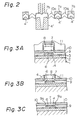
- the second embodiment of the present invention will now be described with reference to Fig. 2.
- the second embodiment is substantially the same as the first embodiment described hereinbefore, except for the configuration of the conductor pattern.
- conductors 4 (shown in dotted lines) are stripe-shaped, as illustrated in Fig. 1G.
- conductors 4' are square land-shaped.
- Conductors 4' can be formed by forming resist pattern 8 into a configuration corresponding to that of conductors 4' in the process illustrated in Figs. 1B and 1C.
- the square land-shaped conductor 4' makes it possible to reduce the influence of the eddy current produced by the magnetic flux caused by the permalloy pattern.
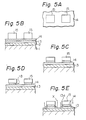
- the third embodiment of the present invention will now be described with reference to Figs. 3A through 3C.
- the third embodiment is also substantially the same as the first embodiment described hereinbefore, except for a process performed between the stage illustrated in Fig. 1D and the stage illustrated in Fig. 1E, that is, a process of lift-off of resist pattern 8.
- the lift-off process is performed merely by scrubbing resist pattern 8 with the aid of a resolvent.
- the lift-off may not be easy, because resist pattern 8 is covered with insulating layer 9 and permalloy layer 10.
- this problem can be resolved in the following manner. Namely, after permalloy layer 10 has been formed as illustrated in Fig.
- resin layer 11 of, for example, AZ type, polyimide type, or polyladder- siloxane type resist material is formed on permalloy layer 10, as illustrated in Fig. 3A.
- Resin layer 11 is 1.5 pm thick at the portion formed on the flat surface of permalloy layer 10 and 0.25 um thick at the portion formed on permalloy layer 10 deposited on resist pattern 8.
- the entire surface of the device is ion etched. Since the ion etching process is poor in selective etch characteristics, the surface to be etched is lowered with the original shape being substantially maintained. The ion etching process is performed until the surface of resist pattern 8 has been exposed.
- a scrubbing process is used with the aid of a resolvent to remove resist pattern 8 and resin layer 11.
- the rising portions of insulating layer 9 and permalloy layer 10 are also removed, and, accordingly, a flat pattern forming layer as illustrated in Fig. 3C is formed.
- the stage illustrated in Fig. 3C corresponds to that illustrated in Fig. 1E.
- a permalloy propagation pattern of pattern elements 14a and 16a is formed as illustrated in Fig. 4H.
- Figs. 4A, 4G and 4H are plan views of a magnetic bubble memory device and Figs. 4B through 4F are sectional views.
- permalloy layer 14 is formed on permalloy layer 14.
- An ion etching process is used to pattern permalloy layer 14 so as to form permalloy portions 14, from which pattern elements 14a are formed, as will be described hereinafter.
- an ion etching process is used to etch the surface of insulating layer 13.
- spatters of insulating material Si0 2 which are struck out from insulating layer 13 by ions (shown in arrows X), are deposited on the side surfaces of permalloy portions 14, thereby forming walls 13a.
- Walls 13a are 0.1 ⁇ .1m thick, for example, and act as spacers which provide gaps between pattern elements 14a and 16a, as described hereinafter.
- permalloy layer 16 is formed by vapor deposition or spattering. Resist pattern 15 is then lifted off. Consequently, as illustrated in Figs. 4F and 4G, a pattern forming layer is formed which has permalloy portions 14 and 16 with spacer portions 13a therebetween. In the illustrated embodiment, there is a step between the surfaces of permalloy portions 14 and 16. This step, if undesirable, can be eliminated by depositing insulating materials, such as SiO or Cr 2 0 3 , on the etched surface of insulating layer 13 by vapor deposition, prior to the process of forming permalloy layer 16 illustrated in Fig. 4E.
- insulating materials such as SiO or Cr 2 0 3
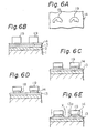
- FIG. 5A through 51 illustrate the fifth embodiment of the present invention, which is similar to the fourth embodiment described hereinbefore.
- a chemical etching process is used to provide permalloy portions 14 with 0.1 pm undercuts 18 as illustrated in Fig. 5D.
- This etching process employs an etchant composed of HN0 3 (500 cc), H 2 0 (500 cc), and FeCI (2.5 g) and is performed for 5 seconds at 25°C.
- HN0 3 500 cc
- H 2 0 500 cc
- FeCI 2.5 g
- insulating layer 13 is ion etched, so that insulating materials Si0 2 are spattered on the undercut surfaces of permalloy portions 14 to form walls 13a.
- walls 13a can be formed by an etching amount less than that in the fourth embodiment.
- Figure 7 illustrates the relationship between the etching amount and the depositing amount of Si0 2 on the undercut portion when insulating layer 13 is ion etched, wherein the abscissa indicates the etching amount and the ordinate indicates the depositing amount.
- the embodiment illustrated is that in the case of a 1000 A undercut. It will be understood that the depositing amount efficiently increases until it reaches the size of the undercut (shown by the point "P").
- FIGs 6A through 61 illustrate the sixth embodiment of the present invention, which is substantially the same as the fifth embodiment described hereinbefore.
- resist pattern 19 formed on permalloy layer 14 has a configuration which substantially corresponds to the half disk-shaped configuration of pattern elements 14a.
- permalloy portions 14 in the pattern forming layer are in the form of pattern elements 14a, and resist pattern RP is formed on the pattern forming layer so as to be registered with permalloy portions 14.
- an embodiment of the present invention can make it possible to form a pattern of metal elements with very small gaps of size less than 1 ⁇ .1m therebetween, with the aid of conventional photolithographic techniques.
Landscapes
- Engineering & Computer Science (AREA)
- Power Engineering (AREA)
- Physics & Mathematics (AREA)
- General Physics & Mathematics (AREA)
- Manufacturing & Machinery (AREA)
- Thin Magnetic Films (AREA)
- Hall/Mr Elements (AREA)
Claims (7)
Applications Claiming Priority (2)
| Application Number | Priority Date | Filing Date | Title |
|---|---|---|---|
| JP56098371A JPS581878A (ja) | 1981-06-26 | 1981-06-26 | 磁気バブルメモリ素子の製造方法 |
| JP98371/81 | 1981-06-26 |
Publications (2)
| Publication Number | Publication Date |
|---|---|
| EP0068846A1 EP0068846A1 (de) | 1983-01-05 |
| EP0068846B1 true EP0068846B1 (de) | 1985-10-16 |
Family
ID=14218015
Family Applications (1)
| Application Number | Title | Priority Date | Filing Date |
|---|---|---|---|
| EP82303330A Expired EP0068846B1 (de) | 1981-06-26 | 1982-06-25 | Verfahren zum Herstellen eines Musters aus Metallelementen auf einem Substrat |
Country Status (5)
| Country | Link |
|---|---|
| US (1) | US4464459A (de) |
| EP (1) | EP0068846B1 (de) |
| JP (1) | JPS581878A (de) |
| CA (1) | CA1189985A (de) |
| DE (1) | DE3266920D1 (de) |
Families Citing this family (14)
| Publication number | Priority date | Publication date | Assignee | Title |
|---|---|---|---|---|
| EP0229397B1 (de) * | 1986-01-06 | 1995-08-09 | Semiconductor Energy Laboratory Co., Ltd. | Photoelektrische Umwandlungsvorrichtung und ihr Herstellungsverfahren |
| JPS62121893U (de) * | 1986-01-27 | 1987-08-03 | ||
| JPH0761189B2 (ja) * | 1986-03-20 | 1995-06-28 | ヘンリイ オリバ− ウオルコツト | 電気音響トランスジユ−サ装置 |
| US5017509A (en) * | 1988-07-19 | 1991-05-21 | Regents Of The University Of California | Stand-off transmission lines and method for making same |
| JPH0264295U (de) * | 1988-11-04 | 1990-05-15 | ||
| JPH02112095U (de) * | 1989-02-27 | 1990-09-07 | ||
| JPH02143897U (de) * | 1989-05-09 | 1990-12-06 | ||
| US5120668A (en) * | 1991-07-10 | 1992-06-09 | Ibm Corporation | Method of forming an inverse T-gate FET transistor |
| US5516625A (en) * | 1993-09-08 | 1996-05-14 | Harris Corporation | Fill and etchback process using dual photoresist sacrificial layer and two-step etching process for planarizing oxide-filled shallow trench structure |
| KR0134108B1 (ko) * | 1994-06-30 | 1998-04-20 | 김주용 | 반도체 소자의 제조방법 |
| US6178066B1 (en) | 1998-05-27 | 2001-01-23 | Read-Rite Corporation | Method of fabricating an improved thin film device having a small element with well defined corners |
| TWI338171B (en) * | 2005-05-02 | 2011-03-01 | Au Optronics Corp | Display device and wiring structure and method for forming the same |
| JP2008293609A (ja) * | 2007-05-25 | 2008-12-04 | Fujitsu Ltd | 複製用型の製造方法、ナノホール構造体の製造方法、及び磁気記録媒体の製造方法 |
| FR2927469B1 (fr) * | 2008-02-13 | 2010-04-16 | Commissariat Energie Atomique | Procede pour realiser un nanocontact d'une vanne de spin entrant dans la constitution d'un oscillateur radio freqence. |
Family Cites Families (11)
| Publication number | Priority date | Publication date | Assignee | Title |
|---|---|---|---|---|
| DE2063726C3 (de) * | 1970-12-24 | 1979-09-06 | Licentia Patent-Verwaltungs-Gmbh, 6000 Frankfurt | Verfahren zum Herstellen eines Halbleiterbauelements |
| US3924319A (en) * | 1974-08-12 | 1975-12-09 | Bell Telephone Labor Inc | Method of fabricating stepped electrodes |
| GB1543845A (en) * | 1975-05-27 | 1979-04-11 | Fairchild Camera Instr Co | Production of a narrow opening to a surface of a material |
| NL7506594A (nl) * | 1975-06-04 | 1976-12-07 | Philips Nv | Werkwijze voor het vervaardigen van een halfge- leiderinrichting en halfgeleiderinrichting ver- vaardigd met behulp van de werkwijze. |
| US4251571A (en) * | 1978-05-02 | 1981-02-17 | International Business Machines Corporation | Method for forming semiconductor structure with improved isolation between two layers of polycrystalline silicon |
| EP0007805B1 (de) * | 1978-07-29 | 1983-02-16 | Fujitsu Limited | Verfahren zur Beschichtung der Seitenwände von Halbleiterbauteilen |
| US4209350A (en) * | 1978-11-03 | 1980-06-24 | International Business Machines Corporation | Method for forming diffusions having narrow dimensions utilizing reactive ion etching |
| JPS5595340A (en) * | 1979-01-10 | 1980-07-19 | Chiyou Lsi Gijutsu Kenkyu Kumiai | Preparation of semiconductor device |
| IT1140645B (it) * | 1979-03-05 | 1986-10-01 | Rca Corp | Materiale composito di passivazione per un dispositivo semiconduttore comprendente uno strato di nitruro di silicio (si alla terza in alla quarta) ed uno strato di vetro al fosfosilicato (psg) e metodo di fabbricazione delle stesso |
| US4376137A (en) * | 1979-08-31 | 1983-03-08 | Rockwell International Corporation | Method of fabricating a bi-level magnetic bubble propagation circuit |
| US4251319A (en) * | 1979-12-21 | 1981-02-17 | Control Data Corporation | Bubble memory chip and method for manufacture |
-
1981
- 1981-06-26 JP JP56098371A patent/JPS581878A/ja active Granted
-
1982
- 1982-06-23 CA CA000405866A patent/CA1189985A/en not_active Expired
- 1982-06-25 US US06/392,173 patent/US4464459A/en not_active Expired - Fee Related
- 1982-06-25 EP EP82303330A patent/EP0068846B1/de not_active Expired
- 1982-06-25 DE DE8282303330T patent/DE3266920D1/de not_active Expired
Also Published As
| Publication number | Publication date |
|---|---|
| DE3266920D1 (en) | 1985-11-21 |
| JPS581878A (ja) | 1983-01-07 |
| JPS613023B2 (de) | 1986-01-29 |
| EP0068846A1 (de) | 1983-01-05 |
| CA1189985A (en) | 1985-07-02 |
| US4464459A (en) | 1984-08-07 |
Similar Documents
| Publication | Publication Date | Title |
|---|---|---|
| US4464459A (en) | Method of forming a pattern of metal elements | |
| US4529686A (en) | Method for the manufacture of extremely fine structures | |
| US5563079A (en) | Method of making a field effect transistor | |
| US4597826A (en) | Method for forming patterns | |
| US7727410B2 (en) | Process for formation of three-dimensional photonic crystal | |
| JP2694857B2 (ja) | 薄膜磁気ヘッドのポールチップ構造の製造方法 | |
| US4614563A (en) | Process for producing multilayer conductor structure | |
| KR0147976B1 (ko) | 박막 헤드의 패턴 평탄화 방법 | |
| EP0011135B1 (de) | Verfahren zur Herstellung einer Magnetblasen-Vorrichtung und nach diesem Verfahren hergestellte Vorrichtung | |
| JP2501873B2 (ja) | 薄膜磁気ヘッドの製造方法 | |
| EP0779556A2 (de) | Verfahren zur Herstellung einer Halbleiteranordnung | |
| JPH03105712A (ja) | 薄膜層にオーディオ、ビデオ及びコンピュータ用磁気ヘッドのポール・ピース及びギャップを形成する方法 | |
| KR0147996B1 (ko) | 박막 헤드의 패턴 평탄화 방법 | |
| EP0022580A1 (de) | Herstellungsverfahren von auf magnetische Eigenschaften basierten Vorrichtungen | |
| JP2564284B2 (ja) | 薄膜コイルの製造方法 | |
| US4334950A (en) | Advantageous fabrication technique for devices relying on magnetic properties | |
| KR0174460B1 (ko) | 박막 자기 헤드의 하부 자성층 패턴 형성 방법 | |
| CA1088382A (en) | Method of making a large scale integrated device having a planar surface | |
| JPH04281205A (ja) | エッチング方法 | |
| CA1135852A (en) | Bubble memory chip and method for manufacture | |
| JPH03132909A (ja) | レジストパターンの形成方法 | |
| JPS5850618A (ja) | 薄膜磁気ヘツド | |
| JPH01173308A (ja) | 薄膜磁気ヘッドの製造方法 | |
| JPH04281204A (ja) | エッチング方法 | |
| JPS63160006A (ja) | 薄膜磁気ヘツドおよびその製造方法 |
Legal Events
| Date | Code | Title | Description |
|---|---|---|---|
| PUAI | Public reference made under article 153(3) epc to a published international application that has entered the european phase |
Free format text: ORIGINAL CODE: 0009012 |
|
| AK | Designated contracting states |
Designated state(s): DE FR GB NL |
|
| 17P | Request for examination filed |
Effective date: 19830624 |
|
| GRAA | (expected) grant |
Free format text: ORIGINAL CODE: 0009210 |
|
| AK | Designated contracting states |
Designated state(s): DE FR GB NL |
|
| REF | Corresponds to: |
Ref document number: 3266920 Country of ref document: DE Date of ref document: 19851121 |
|
| ET | Fr: translation filed | ||
| PLBE | No opposition filed within time limit |
Free format text: ORIGINAL CODE: 0009261 |
|
| STAA | Information on the status of an ep patent application or granted ep patent |
Free format text: STATUS: NO OPPOSITION FILED WITHIN TIME LIMIT |
|
| 26N | No opposition filed | ||
| PGFP | Annual fee paid to national office [announced via postgrant information from national office to epo] |
Ref country code: GB Payment date: 19890531 Year of fee payment: 8 |
|
| PGFP | Annual fee paid to national office [announced via postgrant information from national office to epo] |
Ref country code: FR Payment date: 19890629 Year of fee payment: 8 |
|
| PGFP | Annual fee paid to national office [announced via postgrant information from national office to epo] |
Ref country code: NL Payment date: 19890630 Year of fee payment: 8 |
|
| PGFP | Annual fee paid to national office [announced via postgrant information from national office to epo] |
Ref country code: DE Payment date: 19890824 Year of fee payment: 8 |
|
| PG25 | Lapsed in a contracting state [announced via postgrant information from national office to epo] |
Ref country code: GB Effective date: 19900625 |
|
| PG25 | Lapsed in a contracting state [announced via postgrant information from national office to epo] |
Ref country code: NL Effective date: 19910101 |
|
| NLV4 | Nl: lapsed or anulled due to non-payment of the annual fee | ||
| GBPC | Gb: european patent ceased through non-payment of renewal fee | ||
| PG25 | Lapsed in a contracting state [announced via postgrant information from national office to epo] |
Ref country code: FR Effective date: 19910228 |
|
| PG25 | Lapsed in a contracting state [announced via postgrant information from national office to epo] |
Ref country code: DE Effective date: 19910301 |
|
| REG | Reference to a national code |
Ref country code: FR Ref legal event code: ST |