EP0053014A1 - Circuit de générateur de signaux d'horloge - Google Patents
Circuit de générateur de signaux d'horloge Download PDFInfo
- Publication number
- EP0053014A1 EP0053014A1 EP81305484A EP81305484A EP0053014A1 EP 0053014 A1 EP0053014 A1 EP 0053014A1 EP 81305484 A EP81305484 A EP 81305484A EP 81305484 A EP81305484 A EP 81305484A EP 0053014 A1 EP0053014 A1 EP 0053014A1
- Authority
- EP
- European Patent Office
- Prior art keywords
- circuit
- clock signal
- clock
- potential
- logic
- Prior art date
- Legal status (The legal status is an assumption and is not a legal conclusion. Google has not performed a legal analysis and makes no representation as to the accuracy of the status listed.)
- Granted
Links
Images

Classifications
-
- H—ELECTRICITY
- H03—ELECTRONIC CIRCUITRY
- H03K—PULSE TECHNIQUE
- H03K5/00—Manipulating of pulses not covered by one of the other main groups of this subclass
- H03K5/15—Arrangements in which pulses are delivered at different times at several outputs, i.e. pulse distributors
- H03K5/151—Arrangements in which pulses are delivered at different times at several outputs, i.e. pulse distributors with two complementary outputs
- H03K5/1515—Arrangements in which pulses are delivered at different times at several outputs, i.e. pulse distributors with two complementary outputs non-overlapping
Definitions
- the present invention relates to a clock generator circuit for generating two pairs of clock signals by using a reference clock signal.
- clock signals that is, two pairs of clock signals are used.
- clock signals are used in a switched capacitor integrator.
- One conventional clock generator circuit comprises a pair of NOR circuits cross-coupled to each other, which serve as an R-S flip-flop. This clock generator circuit generates two non-overlapping clock signals and ⁇ 2 opposite in phase to each other. (See: Electronics, page 99, January 20, 1977.)
- this circuit when an inverter is connected to the output terminal of each of the NOR circuits, two inverted clock signals 1 and 0 2 of the clock signals ⁇ 1 and ⁇ 2 are also obtained.
- the clock generator circuit associated with such inverters generates two pairs of clock signals ⁇ 1 and ⁇ 1 , and ⁇ 2 and ⁇ 2 .
- a clock generator circuit for generating two pairs of clock signals by using a reference clock signal, comprising: first and second logic circuits, each having first and second input terminals and an output terminal, for generating first and second clock signals, respectively, the first input terminal of each of the first and second logic circuits receiving the reference clock signal; a first delay circuit, connected between the output terminal of the first logic circuit and the the second input terminal of the second logic circuit, for delaying and inverting the first clock signal so as to generate a third clock signal which forms a pair with the first clock signal; a second delay circuit, connected between the output terminal of the second logic circuit and the second input terminal of the first logic circuit, for delaying and inverting the second clock signal so as to generate a fourth clock signal which forms a pair with the second clock signal; the first logic circuit detecting a change or the potential of the fourth clock signal so as to change the potential of the first clock signal, when the potential of the reference clock signal is high; and the second logic circuit detecting a change of the potential of
- Fig. 1 which illustrates a general switched capacitor integrator
- SW 1 and SW 2 are switches; C 1 and C are capacitors; and OP is an operational amplifier.
- the capacitor C 2 forms a negative feedback path of the operational amplifier OP.
- the switch SW 1 When the switch SW 1 is turned on, the capacitor C 1 is charged by an input voltage V in . After that, at the next timing, the switch SW 1 is turned off and, in turn, the switch SW 2 is turned on. As a result, the charges stored in the capacitor C 1 are moved to the capacitor C 2 . Since the operational amplifier OP operates so as to hold its input terminal (-) at the ground level, an output voltage V out appears in accordance with the quantity of the charges stored in the capacitor C 1 .
- the input voltage V in is sampled by repeating the above-mentioned operation at a frequency of, for example, 128 kHz, so that the output voltage V out , corresponding tc an integrated value of the sampled voltages, is obtained.
- each of the switches SW and SW 2 comprises a CMOS (Complementary MOS) circuit formed by a p-channel type transistor and a n-channel type transistor. Therefore, when the potential of a clock signal ⁇ 1 and the potential of its inverted signal ⁇ 1 are high and low, respectively, the switch SW 1 is turned on, while, when the potential of each of the signals ⁇ 1 and ⁇ 1 are low and high, respectively, the switch SW 1 is turned off. Similarly, when the potential of a clock signal ⁇ 2 and the potential of its inverted signal ⁇ 2 are high and low, respectively, the switch SW 2 is turned on, while, when the potential of each of the signals ⁇ 2 and ⁇ 2 are low and high, respectively, the switch SW 2 is turned off.
- CMOS Complementary MOS
- switches SW 1 and SW 2 should not be simultaneously turned on. If the switches SW 1 and SW 2 are simultaneously turned on, the capacitor C 2 is charged directly by the input voltage V in and as a result, a normal integration operation can not be performed.
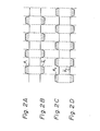
- Figs. 2A through 2D are timing diagrams showing the signals appearing in the circuit of Fig. 1.
- a pair of the clock signals ⁇ 1 and ⁇ 1 are non-overlapped with the other pair of the clock signals ⁇ 2 and ⁇ 2 .
- the high potential of the clock signal ⁇ 1 is non-overlapped with the high potential of the clock signal ⁇ 2 and the low potential of the clock signal ⁇ 2 .
- the low potential of the clock signal ⁇ 1 is non-overlapped with the high potential of the clock signal ⁇ 2 and the low potential of the clock signal ⁇ 2 .
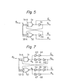
- Fig. 3 is a logic circuit diagram illustrating one conventional clock generator circuit.
- the clock generator circuit comprises two NOR circuits 31 and 32 cross-coupled to each other which serve as an R-S flip-flop.
- the NOR circuit 31 receives a reference clock signal ⁇ 0 directly, while the NOR circuit 32 receives the reference clock signal ⁇ 0 via an inverter 33.
- Each of the NOR circuits 31 generates clock signals ⁇ 1 and ⁇ 2 , respectively, and in addition, clock signals ⁇ 1 and ⁇ 2 are obtained by inverting the clock signals ⁇ 1 and ⁇ 2 , respectively.
- two inverters 34 and 35 are provided.
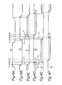
- FIGS. 4A through 4F are timing diagrams showing the signals in the circuit of Fig. 3. Referring to Figs. 4A through 4F, the operation of the circuit of Fig. 3 will now be explained.
- a time t 1 the potential of the reference clock signal ⁇ 0 is changed from low to high, as illustrated in Fig. 4A and, in turn, at a time t 2 the potential of a signal ⁇ 0 is changed from high to low, as illustrated in Fig. 4B.
- the NOR circuit 31 detects the change of the potential at an input terminal 31-A thereof,so that, at a time t 3 , the potential of the clock signal ⁇ 1 is changed from high to low, as illustrated in Fig. 4C and, in turn, at a time t 4 , the potential of the clock signal ⁇ 1 is changed from low to high, as illustrated in Fig. 4D.
- the potential at an input terminal 32-A of the NOR circuit 32 which is the same as the potential of the signal 0 as illustrated in Fig.
- the NOR circuit 32 detects the change of the potential at an input terminal 32-B thereof, so that, at a time t 5 , the potential of the clock signal ⁇ 2 is changed from low to high, as illustrated in Fig. 4E and, in turn, at a time t 6 , the potential of the clock signal ⁇ 2 is changed from high to low, as illustrated in Fig. 4F.
- the high potential of the clock signal ⁇ 1 is never overlapped with the high potential (clock pulse)of the clock signal ⁇ 2 and the low potential of the clock signal ⁇ 2 .
- the clock signal ⁇ 1 as illustrated in Figs. 4D, 4E and 4F, if ⁇ 1 > ⁇ 2 where T is a delay time of the inverter 34 and ⁇ 2 is a delay time of the NOR circuit 32, the low potential of the clock signal ⁇ 1 is overlapped with the high potential of the clock si al ⁇ 2 .
- T3 is a delay time of the inverter 35
- the low potential ⁇ 1 is also overlapped with the low potential of the clock signal ⁇ 2 .
- the delay time ⁇ 1 of the inverter circuit 34 and the delay time ⁇ 3 of the inverter 35 are often fluctuated due to fluctuation in manufacture. Accordingly, it may happens that T 1 > ⁇ 2 (or ⁇ 2 + ⁇ 3 ) or ⁇ 3 > ⁇ 4 (or ⁇ 4 + ⁇ 1 ) is satisfied. Thus, in the circuit of Fig. 3, the clock signals ⁇ 1 and ⁇ 1 may be overlapped with the clock signals ⁇ 2 and ⁇ 2 .
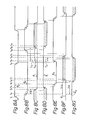
- Fig. 5 is a logic circuit diagram illustrating an embodiment of the clock generator circuit according to the present invention.
- the clock generator circuit comprises a NAND circuit 51 and a NOR circuit 52 cross-coupled to each other, and two inverters 53 and 54.
- a reference clock signal ⁇ 0 is supplied commonly to an input terminal 51-A of the NAND circuit 51 and an input terminal 52-A of the NOR circuit 52.
- the NOR circuit 52 generates a clock signal ⁇ 1 and in turn, the inverter 54 generates a clock signal ⁇ 1 which forms a pair with the clock signal ⁇ 1
- the NAND circuit 51 generates a clock signal ⁇ 2
- the inverter 53 generates a clock signal 2 which forms a pair with the clock signal ⁇ 2 .
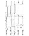
- Figs. 6A through 6E are timing diagrams showing the signals appearing in the circuit of Fig. 5. Referring to Figs. 6A through 6E, the operation of the circuit of Fig. 5 will now be explained.
- the potential of the reference clock signal ⁇ 0 is changed from low to high, as illustrated in Fig. 6A.
- the NOR circuit 52 detects the change of the potential at the input terminal 52-A so that, at a time t 2 , the potential of the clock signal ⁇ 1 is changed from high to low as illustrated in Fig.
- the NAND circuit 51 detects the change of the potential at the input terminal 51-B so that, at a time t 4 , the potential of the clock signal 2 is changed from high to low as illustrated in Fig. 6E and, in turn, the potential of the clock signal ⁇ 2 is changed from low tc high as illustrated in Fig. 6D.
- the potential of the reference clock signal ⁇ 0 falls as illustrated in Fig. 6A and after that, at a time t 7 , the potential of the clock signal 2 rises as illustrated in Fig. 6E. And, in turn, at a time t 8 , the potential of the clock signal ⁇ 2 falls as illustrated in Fig. 6D. After that, at a time t 9 , the potential of the clock signal ⁇ 1 rises as illustrated in Fig. 6B and, in turn, at a time t 10 , the potential of the clock signal falls as illustrated in Fig. 6C.
- the high potential of the clock signal 02 is never overlapped with the high potential of the clock signal ⁇ 1 and the low potential of the clock signal ⁇ 1 and, in addition, the low potential of the clock signal ⁇ 2 is never overlapped with the high potential of the clock signal ⁇ 1 and the low potential of the clock signal ⁇ 1 .
- Fig. 7 is a logic circuit diagram illustrating another embodiment of the clock generator circuit according to the present invention.
- inverters 61 through 68 are added to Fig. 5.
- the operation of the circuit of Fig. 7 is similar to that of the circuit of Fig. 5.
- Figs. 8A through 8G are timing diagrams showing the signals appearing in the circuit of Fig. 7. Referring to Figs. 8A through 8G, the operation of the circuit of Fig. 7 will now be explained.
- the potential of the refernece clock signal ⁇ 0 rises as illustrated in Fig. 8A.
- the potential of a signal ⁇ A generated from the NOR circuit 52 falls, as illustrated in Fig. 8B.
- the potential of the clock signal ⁇ 1 falls as illustrated in Fig. 8C and, in turn, at a time t 4 , the potential of the clock signal c 1 rises as illustrated in Fig. 8D.
- ⁇ 11 is the total delay time of the inverters 67 and 68
- T12 is the total delay time of the inverters 54, 65, 66, the NAND circuit 51 and the inverters 53, 61 and 62
- ⁇ 13 is the total delay time of the inverters 54, 65, 66, the NAND circuit 51 and the inverters 63 and 64.
- the potential of the reference clock signal ⁇ 0 falls as illustrated in Fig. 8A.
- the potential of the signal ⁇ B rises as illustrated in Fig. 8E.
- the potential of the clock signal 2 rises as illustrated in Fig. 8G and, in turn, at a time t 11 , the potential of the clock signal ⁇ 2 falls as illustrated in Fig. 8F.
- the potential of the signal ⁇ A rises as illustrated in Fig. 8B.
- the potential of the clock signal rises as illustrated in Fig. 8C and, in turn, at a time t 14 , the potential of the clock signal ⁇ 1 falls as illustrated in Fig. 8D.
- T14 is the total delay of the inverters 63 and 64
- T 15 is the total delay time of the inverters 53, 61 and 62, the NOR circuit 52 and the inverters 67 and 68
- L16 is the total delay time of the ivnerters 53, 61 and 62, the NOR circuit 52 and the inverters 54, 65 and 66.
- the clock generator circuit for generating two pairs of clock signals according to the present invention has an advantage in that a pair of clock signals are not overlapped with another pair of clock signals. Therefore, when the clock signals obtained by the clock generator circuit according to the present invention are applied to the switches SW 1 and SW 2 of the switched capacitor integrator of Fig. 1, the switched capacitor integrator can perform a reliable integration operation.
Applications Claiming Priority (2)
| Application Number | Priority Date | Filing Date | Title |
|---|---|---|---|
| JP55163607A JPS5787620A (en) | 1980-11-20 | 1980-11-20 | Clock generating circuit |
| JP163607/80 | 1980-11-20 |
Publications (2)
| Publication Number | Publication Date |
|---|---|
| EP0053014A1 true EP0053014A1 (fr) | 1982-06-02 |
| EP0053014B1 EP0053014B1 (fr) | 1985-04-03 |
Family
ID=15777138
Family Applications (1)
| Application Number | Title | Priority Date | Filing Date |
|---|---|---|---|
| EP81305484A Expired EP0053014B1 (fr) | 1980-11-20 | 1981-11-20 | Circuit de générateur de signaux d'horloge |
Country Status (5)
| Country | Link |
|---|---|
| US (1) | US4417158A (fr) |
| EP (1) | EP0053014B1 (fr) |
| JP (1) | JPS5787620A (fr) |
| DE (1) | DE3169742D1 (fr) |
| IE (1) | IE52355B1 (fr) |
Cited By (7)
| Publication number | Priority date | Publication date | Assignee | Title |
|---|---|---|---|---|
| FR2597681A1 (fr) * | 1986-04-18 | 1987-10-23 | Sgs Microelettronica Spa | Systeme anti-chevauchement de phases pour circuits integres mos, en particulier pour le controle de filtres a capacites commutees. |
| US5126588A (en) * | 1987-03-16 | 1992-06-30 | Sgs-Thomson Microelectronics Gmbh | Digital push-pull driver circuit |
| US5376891A (en) * | 1991-10-29 | 1994-12-27 | Sgs-Thomson Microelectronics Gmbh | Phase-sensitive rectifier arrangement with integration effect |
| FR2707059A1 (fr) * | 1993-06-26 | 1994-12-30 | Itt Ind Gmbh Deutsche | |
| EP0714168A3 (fr) * | 1994-11-23 | 1997-06-18 | Texas Instruments Inc | Réduction des courants transversal des circuits électroniques |
| EP0840451A1 (fr) * | 1996-10-30 | 1998-05-06 | STMicroelectronics S.r.l. | Circuit générateur pour générer des signaux sans chevauchement |
| DE10142657A1 (de) * | 2001-08-31 | 2003-03-27 | Infineon Technologies Ag | Schaltungsanordnung zur Erzeugung nicht-überlappender Taktphasen |
Families Citing this family (34)
| Publication number | Priority date | Publication date | Assignee | Title |
|---|---|---|---|---|
| JPS6074815A (ja) * | 1983-09-30 | 1985-04-27 | Nec Corp | スイツチト・キヤパシタ回路のクロツク発生回路 |
| JPS60180321A (ja) * | 1984-02-28 | 1985-09-14 | Nec Corp | クロック信号発生回路 |
| US4689575A (en) * | 1985-07-15 | 1987-08-25 | Rca Corporation | Clock synchronization circuit for a computer timer |
| US4694197A (en) * | 1986-01-06 | 1987-09-15 | Rca Corporation | Control signal generator |
| EP0262412A1 (fr) * | 1986-09-01 | 1988-04-06 | Siemens Aktiengesellschaft | Générateur d'horloge adapté à la charge, réalisé en circuits CMOS |
| JPS63110811A (ja) * | 1986-10-28 | 1988-05-16 | Mitsubishi Electric Corp | クロツクジエネレ−タ |
| JPS63136815A (ja) * | 1986-11-28 | 1988-06-09 | Mitsubishi Electric Corp | 周期信号発生回路 |
| US4816700A (en) * | 1987-12-16 | 1989-03-28 | Intel Corporation | Two-phase non-overlapping clock generator |
| JPH01183211A (ja) * | 1988-01-18 | 1989-07-21 | Sharp Corp | 信号保持回路 |
| JPH03185921A (ja) * | 1989-12-14 | 1991-08-13 | Toshiba Corp | 半導体集積回路 |
| US5057701A (en) * | 1990-02-13 | 1991-10-15 | Hewlett-Packard Company | High speed low skew clock circuit |
| US5055705A (en) * | 1990-02-15 | 1991-10-08 | National Semiconductor Corp. | Selecting one of a plurality of voltages without overlap |
| US5086236A (en) * | 1990-08-27 | 1992-02-04 | Advanced Micro Devices, Inc. | Synchronizing circuit of two clock signals |
| DE69232949T2 (de) * | 1991-11-20 | 2003-08-28 | Fujitsu Ltd | Löschbare Flash-Halbleiterspeichervorrichtung |
| US5378950A (en) * | 1992-02-03 | 1995-01-03 | Kabushiki Kaisha Toshiba | Semiconductor integrated circuit for producing activation signals at different cycle times |
| US5444405A (en) * | 1992-03-02 | 1995-08-22 | Seiko Epson Corporation | Clock generator with programmable non-overlapping clock edge capability |
| JP3441780B2 (ja) * | 1994-02-21 | 2003-09-02 | 日本テキサス・インスツルメンツ株式会社 | クロック信号生成回路 |
| US5517147A (en) * | 1994-11-17 | 1996-05-14 | Unisys Corporation | Multiple-phase clock signal generator for integrated circuits, comprising PLL, counter, and logic circuits |
| KR0139661B1 (ko) * | 1995-04-06 | 1998-07-15 | 문정환 | 비중첩 신호 발생 회로 |
| US6246278B1 (en) * | 1995-12-22 | 2001-06-12 | Lsi Logic Corporation | High speed single phase to dual phase clock divider |
| WO1997042707A1 (fr) * | 1996-05-06 | 1997-11-13 | Siemens Aktiengesellschaft | Generateur de signal d'horloge |
| JP2877205B2 (ja) * | 1996-08-28 | 1999-03-31 | 日本電気株式会社 | 2相ノンオーバラップ信号生成回路 |
| DE19753279C2 (de) | 1997-12-01 | 2001-03-08 | Sgs Thomson Microelectronics | Elektrische Schaltung mit mindestens einem geschalteten Kondensator und Verfahren zum Betreiben dieser Schaltung |
| US6304125B1 (en) * | 1998-09-04 | 2001-10-16 | Sun Microsystems, Inc. | Method for generating and distribution of polyphase clock signals |
| US6188262B1 (en) * | 1998-09-04 | 2001-02-13 | Sun Microsystems, Inc. | Synchronous polyphase clock distribution system |
| JP2002026265A (ja) * | 2000-07-06 | 2002-01-25 | Toshiba Lsi System Support Kk | 半導体集積回路およびその配置設計方法 |
| US6542017B2 (en) * | 2001-06-13 | 2003-04-01 | Texas Instruments Incorporated | Feed-forward approach for timing skew in interleaved and double-sampled circuits |
| US6798248B2 (en) * | 2002-12-20 | 2004-09-28 | Intel Corporation | Non-overlapping clock generation |
| KR100526350B1 (ko) * | 2003-08-23 | 2005-11-08 | 삼성전자주식회사 | 다상 클록신호 발생회로 및 방법 |
| JP4143054B2 (ja) * | 2004-08-19 | 2008-09-03 | 株式会社東芝 | 電圧生成回路 |
| CN100338875C (zh) * | 2004-11-12 | 2007-09-19 | 鸿富锦精密工业(深圳)有限公司 | 时钟信号发生器 |
| US7612595B2 (en) * | 2006-09-19 | 2009-11-03 | Melexis Tessenderlo Nv | Sequence independent non-overlapping digital signal generator with programmable delay |
| JP2010038780A (ja) * | 2008-08-06 | 2010-02-18 | Sanyo Electric Co Ltd | 周波数検出回路 |
| US11451217B2 (en) * | 2019-10-28 | 2022-09-20 | Taiwan Semiconductor Manufacturing Company, Ltd. | Match-slave latch with skewed clock |
Citations (8)
| Publication number | Priority date | Publication date | Assignee | Title |
|---|---|---|---|---|
| FR2064528A5 (fr) * | 1969-09-22 | 1971-07-23 | Compteurs Comp D | |
| US3668436A (en) * | 1969-12-15 | 1972-06-06 | Computer Design Corp | Circuit apparatus for supplying first and second trains of mutually exclusive clock pulses |
| US3858061A (en) * | 1972-12-27 | 1974-12-31 | Ibm | Multiple size gates on fet chips |
| US3961269A (en) * | 1975-05-22 | 1976-06-01 | Teletype Corporation | Multiple phase clock generator |
| US4066919A (en) * | 1976-04-01 | 1978-01-03 | Motorola, Inc. | Sample and hold circuit |
| FR2379198A1 (fr) * | 1977-01-28 | 1978-08-25 | Thomson Csf | Horloge logique diphasee |
| US4140927A (en) * | 1977-04-04 | 1979-02-20 | Teletype Corporation | Non-overlapping clock generator |
| GB2030403A (en) * | 1978-08-30 | 1980-04-02 | Siemens Ag | Pulse converter |
Family Cites Families (3)
| Publication number | Priority date | Publication date | Assignee | Title |
|---|---|---|---|---|
| US3311754A (en) * | 1964-02-06 | 1967-03-28 | Richard A Linder | Transistorized high speed bistable multivibrator for digital counter bit |
| US3448295A (en) * | 1966-07-26 | 1969-06-03 | Gen Instrument Corp | Four phase clock circuit |
| JPS5737866Y2 (fr) * | 1977-08-22 | 1982-08-20 |
-
1980
- 1980-11-20 JP JP55163607A patent/JPS5787620A/ja active Granted
-
1981
- 1981-11-18 US US06/322,720 patent/US4417158A/en not_active Expired - Lifetime
- 1981-11-19 IE IE2718/81A patent/IE52355B1/en unknown
- 1981-11-20 DE DE8181305484T patent/DE3169742D1/de not_active Expired
- 1981-11-20 EP EP81305484A patent/EP0053014B1/fr not_active Expired
Patent Citations (8)
| Publication number | Priority date | Publication date | Assignee | Title |
|---|---|---|---|---|
| FR2064528A5 (fr) * | 1969-09-22 | 1971-07-23 | Compteurs Comp D | |
| US3668436A (en) * | 1969-12-15 | 1972-06-06 | Computer Design Corp | Circuit apparatus for supplying first and second trains of mutually exclusive clock pulses |
| US3858061A (en) * | 1972-12-27 | 1974-12-31 | Ibm | Multiple size gates on fet chips |
| US3961269A (en) * | 1975-05-22 | 1976-06-01 | Teletype Corporation | Multiple phase clock generator |
| US4066919A (en) * | 1976-04-01 | 1978-01-03 | Motorola, Inc. | Sample and hold circuit |
| FR2379198A1 (fr) * | 1977-01-28 | 1978-08-25 | Thomson Csf | Horloge logique diphasee |
| US4140927A (en) * | 1977-04-04 | 1979-02-20 | Teletype Corporation | Non-overlapping clock generator |
| GB2030403A (en) * | 1978-08-30 | 1980-04-02 | Siemens Ag | Pulse converter |
Non-Patent Citations (5)
| Title |
|---|
| Electronic Engineering, Vol. 50, No. 616 December 1978 S.J. CAHILL "A Single-Chip Two-Phase Clock" pages 27, 29 * complete article * * |
| Electronics, 20 January 1977 N. HECKT "Two-Phase Clock Features Nonoverlapping Outputs" page 99 * complete article * * |
| IBM Technical Disclosure Bulletin Vol. 20, No. 6, November 1977 F.K. ALLEN "Multiphase Clocking System with Delay Tracking for Control and/or Data Systems" pages 2419 and 2420 * complete article * * |
| PATENT ABSTRACTS OF JAPAN Vol. 2, No. 10, 25 January 1978 page 10409E77; & JP-A-52 127 051 * |
| PATENT ABSTRACTS OF JAPAN Vol. 5, No. 55, 16 April 1981; & JP-A-56 006 525 * |
Cited By (10)
| Publication number | Priority date | Publication date | Assignee | Title |
|---|---|---|---|---|
| FR2597681A1 (fr) * | 1986-04-18 | 1987-10-23 | Sgs Microelettronica Spa | Systeme anti-chevauchement de phases pour circuits integres mos, en particulier pour le controle de filtres a capacites commutees. |
| US5126588A (en) * | 1987-03-16 | 1992-06-30 | Sgs-Thomson Microelectronics Gmbh | Digital push-pull driver circuit |
| US5376891A (en) * | 1991-10-29 | 1994-12-27 | Sgs-Thomson Microelectronics Gmbh | Phase-sensitive rectifier arrangement with integration effect |
| FR2707059A1 (fr) * | 1993-06-26 | 1994-12-30 | Itt Ind Gmbh Deutsche | |
| NL9401042A (nl) * | 1993-06-26 | 1995-01-16 | Itt Ind Gmbh Deutsche | Klokgenererende schakeling voor klokgestuurde logische schakelingen. |
| EP0714168A3 (fr) * | 1994-11-23 | 1997-06-18 | Texas Instruments Inc | Réduction des courants transversal des circuits électroniques |
| EP0840451A1 (fr) * | 1996-10-30 | 1998-05-06 | STMicroelectronics S.r.l. | Circuit générateur pour générer des signaux sans chevauchement |
| DE10142657A1 (de) * | 2001-08-31 | 2003-03-27 | Infineon Technologies Ag | Schaltungsanordnung zur Erzeugung nicht-überlappender Taktphasen |
| US6838922B2 (en) | 2001-08-31 | 2005-01-04 | Infineon Technologies Ag | Circuit arrangement for generating non-overlapping clock phases |
| DE10142657B4 (de) * | 2001-08-31 | 2005-02-24 | Infineon Technologies Ag | Schaltungsanordnung zur Erzeugung nicht-überlappender Taktphasen |
Also Published As
| Publication number | Publication date |
|---|---|
| IE52355B1 (en) | 1987-09-30 |
| EP0053014B1 (fr) | 1985-04-03 |
| JPS5787620A (en) | 1982-06-01 |
| US4417158A (en) | 1983-11-22 |
| IE812718L (en) | 1982-05-20 |
| DE3169742D1 (en) | 1985-05-09 |
| JPH0119298B2 (fr) | 1989-04-11 |
Similar Documents
| Publication | Publication Date | Title |
|---|---|---|
| EP0053014A1 (fr) | Circuit de générateur de signaux d'horloge | |
| EP0735677B1 (fr) | Circuit oscillateur ayant une fréquence d'oscillation indépendante de la tension d'alimentation | |
| CA1060543A (fr) | Survolteur | |
| US4053821A (en) | Voltage multiplier circuit | |
| KR920005486A (ko) | 신호지연회로 및 클록신호발생회로 | |
| US6833745B2 (en) | Signal generator for charge pump in an integrated circuit | |
| US4316158A (en) | R-C Oscillators using plural inverters | |
| US4472645A (en) | Clock circuit for generating non-overlapping pulses | |
| US5469110A (en) | Charge pumping circuit using non-overlapping clock control | |
| EP0069444A2 (fr) | Générateur d'impulsions de commande | |
| JPH05191228A (ja) | 半導体チツプ回路 | |
| KR0168079B1 (ko) | 클럭발생장치 | |
| US4178585A (en) | Analog-to-digital converter | |
| EP0075129B1 (fr) | Circuit électronique pour abaisser ou élever la tension | |
| JP3222308B2 (ja) | 電気信号遅延回路 | |
| JPH0691462B2 (ja) | アナログカウンタ回路 | |
| JP3345209B2 (ja) | 逓倍回路 | |
| KR100432121B1 (ko) | 펄스 중심 감지 회로 | |
| JPH0677781A (ja) | 発振回路 | |
| US5861765A (en) | Analogue delay circuit with a constant delay time | |
| US6369587B1 (en) | Pulse center detection circuit | |
| EP0704969B1 (fr) | Multivibrateurs astables | |
| KR940008192B1 (ko) | 듀티 50%을 갖는 주파수 체배기 | |
| JP3392278B2 (ja) | 発振器 | |
| KR100207488B1 (ko) | 고 전압 클럭 발생장치 |
Legal Events
| Date | Code | Title | Description |
|---|---|---|---|
| PUAI | Public reference made under article 153(3) epc to a published international application that has entered the european phase |
Free format text: ORIGINAL CODE: 0009012 |
|
| AK | Designated contracting states |
Designated state(s): DE FR GB NL |
|
| 17P | Request for examination filed |
Effective date: 19821130 |
|
| GRAA | (expected) grant |
Free format text: ORIGINAL CODE: 0009210 |
|
| AK | Designated contracting states |
Designated state(s): DE FR GB NL |
|
| REF | Corresponds to: |
Ref document number: 3169742 Country of ref document: DE Date of ref document: 19850509 |
|
| ET | Fr: translation filed | ||
| PLBE | No opposition filed within time limit |
Free format text: ORIGINAL CODE: 0009261 |
|
| STAA | Information on the status of an ep patent application or granted ep patent |
Free format text: STATUS: NO OPPOSITION FILED WITHIN TIME LIMIT |
|
| 26N | No opposition filed | ||
| PGFP | Annual fee paid to national office [announced via postgrant information from national office to epo] |
Ref country code: NL Payment date: 19901130 Year of fee payment: 10 |
|
| PG25 | Lapsed in a contracting state [announced via postgrant information from national office to epo] |
Ref country code: NL Effective date: 19920601 |
|
| NLV4 | Nl: lapsed or anulled due to non-payment of the annual fee | ||
| PGFP | Annual fee paid to national office [announced via postgrant information from national office to epo] |
Ref country code: GB Payment date: 19920903 Year of fee payment: 12 |
|
| PGFP | Annual fee paid to national office [announced via postgrant information from national office to epo] |
Ref country code: FR Payment date: 19921127 Year of fee payment: 12 |
|
| PG25 | Lapsed in a contracting state [announced via postgrant information from national office to epo] |
Ref country code: GB Effective date: 19931120 |
|
| GBPC | Gb: european patent ceased through non-payment of renewal fee |
Effective date: 19931120 |
|
| PG25 | Lapsed in a contracting state [announced via postgrant information from national office to epo] |
Ref country code: FR Effective date: 19940729 |
|
| REG | Reference to a national code |
Ref country code: FR Ref legal event code: ST |
|
| PGFP | Annual fee paid to national office [announced via postgrant information from national office to epo] |
Ref country code: DE Payment date: 19991119 Year of fee payment: 19 |
|
| PG25 | Lapsed in a contracting state [announced via postgrant information from national office to epo] |
Ref country code: DE Free format text: LAPSE BECAUSE OF NON-PAYMENT OF DUE FEES Effective date: 20010801 |