US5057701A - High speed low skew clock circuit - Google Patents
High speed low skew clock circuit Download PDFInfo
- Publication number
- US5057701A US5057701A US07/479,562 US47956290A US5057701A US 5057701 A US5057701 A US 5057701A US 47956290 A US47956290 A US 47956290A US 5057701 A US5057701 A US 5057701A
- Authority
- US
- United States
- Prior art keywords
- true
- false
- output terminal
- transition
- response
- Prior art date
- Legal status (The legal status is an assumption and is not a legal conclusion. Google has not performed a legal analysis and makes no representation as to the accuracy of the status listed.)
- Expired - Fee Related
Links
Images


Classifications
-
- H—ELECTRICITY
- H03—ELECTRONIC CIRCUITRY
- H03K—PULSE TECHNIQUE
- H03K3/00—Circuits for generating electric pulses; Monostable, bistable or multistable circuits
- H03K3/02—Generators characterised by the type of circuit or by the means used for producing pulses
- H03K3/353—Generators characterised by the type of circuit or by the means used for producing pulses by the use, as active elements, of field-effect transistors with internal or external positive feedback
- H03K3/356—Bistable circuits
- H03K3/356104—Bistable circuits using complementary field-effect transistors
- H03K3/356113—Bistable circuits using complementary field-effect transistors using additional transistors in the input circuit
-
- H—ELECTRICITY
- H03—ELECTRONIC CIRCUITRY
- H03K—PULSE TECHNIQUE
- H03K3/00—Circuits for generating electric pulses; Monostable, bistable or multistable circuits
- H03K3/02—Generators characterised by the type of circuit or by the means used for producing pulses
- H03K3/353—Generators characterised by the type of circuit or by the means used for producing pulses by the use, as active elements, of field-effect transistors with internal or external positive feedback
- H03K3/356—Bistable circuits
- H03K3/3565—Bistables with hysteresis, e.g. Schmitt trigger
-
- H—ELECTRICITY
- H03—ELECTRONIC CIRCUITRY
- H03K—PULSE TECHNIQUE
- H03K5/00—Manipulating of pulses not covered by one of the other main groups of this subclass
- H03K5/15—Arrangements in which pulses are delivered at different times at several outputs, i.e. pulse distributors
- H03K5/151—Arrangements in which pulses are delivered at different times at several outputs, i.e. pulse distributors with two complementary outputs
Definitions
- a clock circuit for use in high speed microprocessor and other logic circuits should have fast transitions that occur in a known and reliable relation to each other (such reliability may be termed "low skew"). These desirable properties of high speed and low skew each requires the minimization of internal propagation delay within the clock circuit.
- the actual clock buffer circuitry is driven from an external signal, it would be desirable if the receiver circuitry were as insensitive as possible to the actual levels of the external signal, as well tolerant of drift in those levels.
- CMOS complementary metal-oxide-semiconductor
- the two sides of the differential receiver each produces a respective fast high-to-low transition that is then sent via an associated pair of gain paths to the actual output stage.
- One such pair of gain paths is associated with each side of, or output from, the differential receiver, for a total of four paths in all.
- each path needs only exhibit excellent propagation for a leading edge transitioning in a particular direction at the input of the path, allowing optimization (transistor sizing) to favor that particular leading edge.
- each gain path to achieve approximately half the propagation delay that a corresponding buffer would exhibit if it had to be responsible for active edges in both directions.
- the four gain paths are combined with a latch-like circuit that creates "hard” (i.e., powerful) drive of complementary output clock lines only during the initial period of time when the capacitance of those clock lines needs to be charged. Afterwards, the level of drive is reduced to a holding, or maintenance, level. This can be done, for example, by sensing that the clock line of interest has reached its high state, and then turning off the large transistor doing the hard driving. Another way to do it is to sense that the complementary clock signal has reached its low state. In either scheme, the fact that the complementary clock line is now low is used as part of a cross coupled output latch that keeps a smaller sustaining driver transistor turned on.
- a small signal can be used to abruptly terminate the holding drive, while at the same time the hard drive for the other state of the clock commences. That is, there are low propagation time gain paths for turning hard drives on, and for terminating the holding drive (which are the four set out above), but not a separate one for killing the hard drive. Instead, hard drive removal uses the associated gain path to propagate an active edge whose direction of transition is opposite of what that gain path is optimized for. That hurts nothing, however, since the hard drive need only be removed before the next transition in the clock (a little less than a half-cycle hence), which is long compared to the propagation times, whether optimal or not.
- this scheme avoids the need for a abrupt termination of the hard drive, by letting it go away at a slower rate as soon as it is not needed. This preserves overall minimum propagation time for the control of each transition in the clock, thus producing a high speed low skew clock.
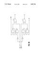
- FIG. 1 is schematic representation of a CMOS differential receiver for clock signals that is constructed in accordance with the principles of the invention
- FIGS. 2A-B are schematic representations of an asymmetric gain buffer and two-level drive output stage constructed in accordance with the principles of the invention.
- FIGS. 3A-B describe an anti-glitch circuit that may be substituted into the circuit of FIGS. 2A-B.
- FIG. 1 wherein is shown a schematic representation of a CMOS differential receiver circuit 1 suitable for being driven from a wide variety of sources, such as the ECL and TTL families of logic.
- the circuit 1 shown in FIG. 1 may be termed a "common gate" differential amplifier that achieves low propagation delay on the high to low transitions of the output signals OUT and NOUT.
- transistors such as Q 5 that have small circles on their gates are P-channel devices, while those such as Q 1 are N-channel devices.
- differential receiver 1 of FIG. 1 The operation of the differential receiver 1 of FIG. 1 is described in detail in the paragraphs that follow.
- Applied to input terminals IN and NIN are an input signal and its complement. These input signals might be intended for use as a clock, a strobe, or perhaps for some other use.
- the actual levels of the input signals need not be known in advance, and these levels may experience a reasonable drift without disturbing the successful operation of the differential receiver circuit 1.
- circuit of FIG. 1 may be implemented without any hysteresis, with hysteresis, or with what may be termed "negative hysteresis", where the circuit anticipates changes in the input signals.
- the Transistors Q 9 and Q 10 are input protection devices for protection from ESD (electro-static discharge).
- Transistor pairs Q 1 /Q 5 and Q 4 /Q 8 form bias circuits producing a bias equal to a single threshold voltage V t .
- Transistors Q 5 and Q 8 act as load resistances for Q 1 and Q 4 , respectively. These bias voltages cause the gate of Q 3 to equal V t plus the voltage V IN applied to IN, and the gate of Q 2 to equal V t plus the voltage applied at NIN. If the input voltage applied to IN is less than that applied to NIN (V NIN ), then the voltage V OUT at OUT will fall rapidly, since the gate voltage of Q 2 will be more than one V t higher than V IN . At the same time Q 7 pulls V NOUT high, since the gate voltage of Q 3 diminished by V NIN is less than V t .
- the ratio of the widths of Q 6 to Q 2 is made larger than the ratio of the widths of Q 5 to Q 1 .
- a similar larger ratio favors the ratio of Q 7 to Q 3 over the ratio of Q 8 to Q 4 .
- the relationship "less than” is substituted for "larger than” in the above.
- "equal to” is substituted for "larger than”.
- the cross coupling of Q 6 and Q 7 reduces the DC load on the input signals IN and NIN. This arises since, for each of the transistor pairs Q 6 /Q 2 and Q 7 /Q 3 , one member of each pair is off whenever the other member of that pair is on. In this connection, it can be observed that the differential receiver circuit 1 of FIG. 1 achieves high voltage gain (CMOS output swings for only one V t swing on the input) without incorporating any appreciable current gain.
- the outputs OUT and NOUT of FIG. 1 are coupled through asymmetric buffers to form separate pull-up and pull-down signal paths. These separate paths are the cascaded series of buffers denoted by reference numerals 2 through 5. Separate pull-up and pull-down paths 2 and 3 are part of a latch-like circuit for generation of the signal CK (Clock) from the signals OUT and NOUT. Similarly, separate pull-up and pull-down paths 4 and 5 are part of a latch-like circuit for generation of the signal NCK from the signals OUT and NOUT. These latch-like circuits involve NOR gates 6 and 7 and the signals CK and NCK, which are generated by circuitry depicted in FIG. 2B.
- path 3 It consists of two cascaded buffers, of which the first is labeled as "N” and the second as "P". This notation means that in the first buffer the N-channel device is large, while its associated P-channel device is small. In the second buffer the P-channel device is large, while its associated N-channel device is small.
- This particular arrangement propagates a rising edge (at the input of the cascaded series) faster than a falling one. It also propagates an input rising edge approximately twice as fast as does a cascaded series of buffers required to minimize propagation delay for both rising and falling edges at the input to the cascaded series.
- Path 2 is similar to path 3, except that it contains an extra stage, so that for an abrupt low to high transition at the input of either path, path 2 produces a corresponding abrupt high to low transition, whereas path 3 would produce an abrupt low to high transition. Note also that within the dotted line denoted by reference numeral 2 is a schematic expansion defining exactly what is meant by this business of "labeled as N" and "labeled as P".
- the FET's in each buffer of the path may be advantageously ratioed in favor of the N-channel or P-channel device whose purpose is to drive the active edge. Which devices these are indicated by the N's and P's in FIG. 2A that label the stages of the separate paths 2 through 5.
- This ratioing is simply the selection of the size of the designated transistor, and is a well known action based, in part, upon the square root of the mobility ratio for the N and P channel materials used in the transistors.
- each of NOR gates 6 and 7 will produce abrupt low to high transitions, but in alternation and occurring at different points in time; that is, the output from the NOR gates 6 and 7 are non-overlapping signals.
- the abrupt low to high transitions from NOR gate 6 produce, with minimum delay (and hence with maximum clock rate and minimum propagation delay), an abrupt high to low transition at the output 8 of path 2 and an abrupt low to high transition at the output 9 of path 3.
- the abrupt low to high transition from NOR gate 7 produces with a minimum of delay an abrupt high to low transition at the output 10 of path 4 and an abrupt low to high transition at the output 11 of path 5.
- FIG. 2B here is what use is made of the various active edges described in connection with FIG. 2A.
- line 8 experiences an abrupt falling edge, it causes transistor 12 to turn on abruptly and transistor 14 to turn off abruptly.
- Transistor 12 is the primary current path for rapidly pulling CK high. (In the two level drive scheme, it is the "hard” driver for CK.)
- an abrupt rising transition on line 11 turns on transistor 19, pulling NCK low, which in turn shuts off transistor 23 and turns on transistor 22.
- Line 9 has meanwhile been low, keeping transistor 13 off (making it safe for transistor 12 to turn on) and keeping transistor 15 on.
- turning transistor 22 on will also contribute current toward the charging of the line capacitance of the CK line, although the primary purpose of the path through transistors 22 and 15 is to maintain CK high once the line capacitance of the CK line is charged and transistor 12 is turned off in anticipation of the next transition in the input signal.
- NCK goes low as CK goes high. This is because lines 8 and 11 originate from a common transition, but experience different numbers of inversion. Thus, when line 8 experiences an abrupt falling edge, line 11 experiences an abrupt rising edge. That, in turn, turns on transistor 19 and causes NCK to go low. That, in turn, is what causes transistor 22 to turn on as mentioned above.
- FIG. 3B illustrates at the gate level what circuitry may be used, while FIG. 3A illustrates the functional equivalent of FIG. 3B.
- NOR gate 6 As shown in FIG. 3A.
- a moments reflection will confirm that the anti-glitching circuit operates by using the rising edge of OUT subsequent to CK's going low to force the output of NOR gate 6 low. That is, the Q output of S/R flip-flop 25 substitutes the rising edge of OUT for the falling edge of CK.
- S/R flip-flop 24 performs a similar function for NOR gate 7 and the signals NOUT and NCK.
- FIG. 3B shows a gate level embodiment that has the same overall functionality as FIG. 3A. Note however, that CK and NCK have been interchanged to avoid the use of extra inverters ahead of their inputs to the cross coupled gates that function as the flip-flops. A further difference between the circuits of FIGS. 3A-B concerns how the hard drive is removed. In FIG. 3A the rising edge of clock removes the hard drive, as discussed in connection with FIGS. 2A-B. In the case of FIG. 3B, the falling on NCK is used to terminate the hard drive of CK.
Landscapes
- Physics & Mathematics (AREA)
- Nonlinear Science (AREA)
- Logic Circuits (AREA)
Abstract
Description
Claims (3)
Priority Applications (3)
| Application Number | Priority Date | Filing Date | Title |
|---|---|---|---|
| US07/479,562 US5057701A (en) | 1990-02-13 | 1990-02-13 | High speed low skew clock circuit |
| EP19910301018 EP0442668A3 (en) | 1990-02-13 | 1991-02-07 | High speed low skew clock circuit |
| JP03041049A JP3143750B2 (en) | 1990-02-13 | 1991-02-13 | Clock circuit |
Applications Claiming Priority (1)
| Application Number | Priority Date | Filing Date | Title |
|---|---|---|---|
| US07/479,562 US5057701A (en) | 1990-02-13 | 1990-02-13 | High speed low skew clock circuit |
Publications (1)
| Publication Number | Publication Date |
|---|---|
| US5057701A true US5057701A (en) | 1991-10-15 |
Family
ID=23904527
Family Applications (1)
| Application Number | Title | Priority Date | Filing Date |
|---|---|---|---|
| US07/479,562 Expired - Fee Related US5057701A (en) | 1990-02-13 | 1990-02-13 | High speed low skew clock circuit |
Country Status (3)
| Country | Link |
|---|---|
| US (1) | US5057701A (en) |
| EP (1) | EP0442668A3 (en) |
| JP (1) | JP3143750B2 (en) |
Cited By (10)
| Publication number | Priority date | Publication date | Assignee | Title |
|---|---|---|---|---|
| US5164619A (en) * | 1990-11-21 | 1992-11-17 | Hewlett-Packard Company | Low skew clocking system for VLSI integrated circuits |
| US5461333A (en) * | 1993-03-15 | 1995-10-24 | At&T Ipm Corp. | Multi-chip modules having chip-to-chip interconnections with reduced signal voltage level and swing |
| US5491443A (en) * | 1994-01-21 | 1996-02-13 | Delco Electronics Corporation | Very low-input capacitance self-biased CMOS buffer amplifier |
| US5631595A (en) * | 1994-09-30 | 1997-05-20 | Lucent Technologies Inc. | Voltage signal line driver comprising a push-pull bridge amplifier |
| US5726596A (en) * | 1996-03-01 | 1998-03-10 | Hewlett-Packard Company | High-performance, low-skew clocking scheme for single-phase, high-frequency global VLSI processor |
| US5760610A (en) * | 1996-03-01 | 1998-06-02 | Hewlett-Packard Company | Qualified universal clock buffer circuit for generating high gain, low skew local clock signals |
| US5777501A (en) * | 1996-04-29 | 1998-07-07 | Mosaid Technologies Incorporated | Digital delay line for a reduced jitter digital delay lock loop |
| US20030038665A1 (en) * | 2001-08-24 | 2003-02-27 | Fujitsu Limited | Distribution of signals in high-speed digital circuitry |
| US20030164720A1 (en) * | 2002-03-01 | 2003-09-04 | Self Paul W. | Differential clock signal detection circuit |
| US6633191B2 (en) | 2001-02-05 | 2003-10-14 | Vitesse Semiconductor Corporation | Clock buffer with DC offset suppression |
Families Citing this family (2)
| Publication number | Priority date | Publication date | Assignee | Title |
|---|---|---|---|---|
| EP0691741B1 (en) * | 1994-07-05 | 2004-10-06 | Matsushita Electric Industrial Co., Ltd. | Latch circuit |
| GB2390945B (en) | 2001-08-24 | 2004-03-10 | Fujitsu Ltd | Switching circuitry |
Citations (2)
| Publication number | Priority date | Publication date | Assignee | Title |
|---|---|---|---|---|
| US4417158A (en) * | 1980-11-20 | 1983-11-22 | Fujitsu Limited | Clock generator circuit |
| US4837505A (en) * | 1985-11-20 | 1989-06-06 | Ricoh Company, Ltd. | Test mode activation circuit |
Family Cites Families (2)
| Publication number | Priority date | Publication date | Assignee | Title |
|---|---|---|---|---|
| US3986046A (en) * | 1972-07-24 | 1976-10-12 | General Instrument Corporation | Dual two-phase clock system |
| EP0262412A1 (en) * | 1986-09-01 | 1988-04-06 | Siemens Aktiengesellschaft | Load-adapted CMOS clock generator |
-
1990
- 1990-02-13 US US07/479,562 patent/US5057701A/en not_active Expired - Fee Related
-
1991
- 1991-02-07 EP EP19910301018 patent/EP0442668A3/en not_active Withdrawn
- 1991-02-13 JP JP03041049A patent/JP3143750B2/en not_active Expired - Fee Related
Patent Citations (2)
| Publication number | Priority date | Publication date | Assignee | Title |
|---|---|---|---|---|
| US4417158A (en) * | 1980-11-20 | 1983-11-22 | Fujitsu Limited | Clock generator circuit |
| US4837505A (en) * | 1985-11-20 | 1989-06-06 | Ricoh Company, Ltd. | Test mode activation circuit |
Cited By (12)
| Publication number | Priority date | Publication date | Assignee | Title |
|---|---|---|---|---|
| US5164619A (en) * | 1990-11-21 | 1992-11-17 | Hewlett-Packard Company | Low skew clocking system for VLSI integrated circuits |
| US5461333A (en) * | 1993-03-15 | 1995-10-24 | At&T Ipm Corp. | Multi-chip modules having chip-to-chip interconnections with reduced signal voltage level and swing |
| US5491443A (en) * | 1994-01-21 | 1996-02-13 | Delco Electronics Corporation | Very low-input capacitance self-biased CMOS buffer amplifier |
| US5631595A (en) * | 1994-09-30 | 1997-05-20 | Lucent Technologies Inc. | Voltage signal line driver comprising a push-pull bridge amplifier |
| US5726596A (en) * | 1996-03-01 | 1998-03-10 | Hewlett-Packard Company | High-performance, low-skew clocking scheme for single-phase, high-frequency global VLSI processor |
| US5760610A (en) * | 1996-03-01 | 1998-06-02 | Hewlett-Packard Company | Qualified universal clock buffer circuit for generating high gain, low skew local clock signals |
| US5777501A (en) * | 1996-04-29 | 1998-07-07 | Mosaid Technologies Incorporated | Digital delay line for a reduced jitter digital delay lock loop |
| US6633191B2 (en) | 2001-02-05 | 2003-10-14 | Vitesse Semiconductor Corporation | Clock buffer with DC offset suppression |
| US20030038665A1 (en) * | 2001-08-24 | 2003-02-27 | Fujitsu Limited | Distribution of signals in high-speed digital circuitry |
| US7096376B2 (en) * | 2001-08-24 | 2006-08-22 | Fujitsu Limited | Device and method for ensuring that a signal always reaches its destination after a fixed number of clock cycles |
| US20030164720A1 (en) * | 2002-03-01 | 2003-09-04 | Self Paul W. | Differential clock signal detection circuit |
| US6977529B2 (en) | 2002-03-01 | 2005-12-20 | Ics Technologies, Inc. | Differential clock signal detection circuit |
Also Published As
| Publication number | Publication date |
|---|---|
| JP3143750B2 (en) | 2001-03-07 |
| EP0442668A3 (en) | 1992-05-20 |
| EP0442668A2 (en) | 1991-08-21 |
| JPH057134A (en) | 1993-01-14 |
Similar Documents
| Publication | Publication Date | Title |
|---|---|---|
| US6121807A (en) | Single phase edge-triggered dual-rail dynamic flip-flop | |
| JP3504172B2 (en) | Cross type voltage level shift circuit | |
| US6633188B1 (en) | Sense amplifier-based flip-flop with asynchronous set and reset | |
| US5334888A (en) | Fast exclusive-or and exclusive-nor gates | |
| EP1446882B1 (en) | Dual-edge triggered dynamic logic | |
| EP0908005B1 (en) | Differential amplifier | |
| EP0265047A1 (en) | Dual domino CMOS logic circuit, including complementary vectorization and integration | |
| US20010050583A1 (en) | High speed latch and flip-flop | |
| US5057701A (en) | High speed low skew clock circuit | |
| WO2001009900A2 (en) | High speed latch and flip-flop | |
| US20020175726A1 (en) | Flip flop circuit | |
| US5532625A (en) | Wave propagation logic | |
| JPH09270683A (en) | Complementary clock generator | |
| US6184718B1 (en) | Dynamic logic circuit | |
| EP0174266B1 (en) | Cmos output buffer | |
| US6225826B1 (en) | Single ended domino compatible dual function generator circuits | |
| US6208186B1 (en) | Differential signal generator | |
| US4897567A (en) | Fast level translator circuit | |
| US6329840B1 (en) | Tristate output buffer with matched signals to PMOS and NMOS output transistors | |
| US20060164147A1 (en) | Level conversion circuit | |
| US6031477A (en) | Differential current switch | |
| US5650735A (en) | Low power, high performance latching interfaces for converting dynamic inputs into static outputs | |
| JP3487631B2 (en) | Electronic circuit with driver circuit | |
| US5864251A (en) | Method and apparatus for self-resetting logic circuitry | |
| US6404253B1 (en) | High speed, low setup time voltage sensing flip-flop |
Legal Events
| Date | Code | Title | Description |
|---|---|---|---|
| AS | Assignment |
Owner name: HEWLETT-PACKARD COMPANY, PALO ALTO, CALIFORNIA A C Free format text: ASSIGNMENT OF ASSIGNORS INTEREST.;ASSIGNOR:MILLER, ROBERT H. JR.;REEL/FRAME:005584/0897 Effective date: 19900213 |
|
| FEPP | Fee payment procedure |
Free format text: PAYOR NUMBER ASSIGNED (ORIGINAL EVENT CODE: ASPN); ENTITY STATUS OF PATENT OWNER: LARGE ENTITY |
|
| FPAY | Fee payment |
Year of fee payment: 4 |
|
| FPAY | Fee payment |
Year of fee payment: 8 |
|
| AS | Assignment |
Owner name: HEWLETT-PACKARD COMPANY, A DELAWARE CORPORATION, C Free format text: MERGER;ASSIGNOR:HEWLETT-PACKARD COMPANY, A CALIFORNIA CORPORATION;REEL/FRAME:010841/0649 Effective date: 19980520 |
|
| AS | Assignment |
Owner name: AGILENT TECHNOLOGIES INC., CALIFORNIA Free format text: ASSIGNMENT OF ASSIGNORS INTEREST;ASSIGNOR:HEWLETT-PACKARD COMPANY, A DELAWARE CORPORATION;REEL/FRAME:010901/0336 Effective date: 20000520 |
|
| REMI | Maintenance fee reminder mailed | ||
| LAPS | Lapse for failure to pay maintenance fees | ||
| STCH | Information on status: patent discontinuation |
Free format text: PATENT EXPIRED DUE TO NONPAYMENT OF MAINTENANCE FEES UNDER 37 CFR 1.362 |
|
| FP | Lapsed due to failure to pay maintenance fee |
Effective date: 20031015 |
|
| AS | Assignment |
Owner name: AVAGO TECHNOLOGIES GENERAL IP (SINGAPORE) PTE. LTD Free format text: ASSIGNMENT OF ASSIGNORS INTEREST;ASSIGNOR:AGILENT TECHNOLOGIES, INC.;REEL/FRAME:017675/0001 Effective date: 20051201 |