EP0045639B1 - Method of forming a microscopic pattern - Google Patents
Method of forming a microscopic pattern Download PDFInfo
- Publication number
- EP0045639B1 EP0045639B1 EP81303514A EP81303514A EP0045639B1 EP 0045639 B1 EP0045639 B1 EP 0045639B1 EP 81303514 A EP81303514 A EP 81303514A EP 81303514 A EP81303514 A EP 81303514A EP 0045639 B1 EP0045639 B1 EP 0045639B1
- Authority
- EP
- European Patent Office
- Prior art keywords
- photoresist
- film
- pattern
- poly
- microscopic pattern
- Prior art date
- Legal status (The legal status is an assumption and is not a legal conclusion. Google has not performed a legal analysis and makes no representation as to the accuracy of the status listed.)
- Expired
Links
Images


Classifications
-
- G—PHYSICS
- G03—PHOTOGRAPHY; CINEMATOGRAPHY; ANALOGOUS TECHNIQUES USING WAVES OTHER THAN OPTICAL WAVES; ELECTROGRAPHY; HOLOGRAPHY
- G03F—PHOTOMECHANICAL PRODUCTION OF TEXTURED OR PATTERNED SURFACES, e.g. FOR PRINTING, FOR PROCESSING OF SEMICONDUCTOR DEVICES; MATERIALS THEREFOR; ORIGINALS THEREFOR; APPARATUS SPECIALLY ADAPTED THEREFOR
- G03F7/00—Photomechanical, e.g. photolithographic, production of textured or patterned surfaces, e.g. printing surfaces; Materials therefor, e.g. comprising photoresists; Apparatus specially adapted therefor
- G03F7/004—Photosensitive materials
- G03F7/038—Macromolecular compounds which are rendered insoluble or differentially wettable
-
- G—PHYSICS
- G03—PHOTOGRAPHY; CINEMATOGRAPHY; ANALOGOUS TECHNIQUES USING WAVES OTHER THAN OPTICAL WAVES; ELECTROGRAPHY; HOLOGRAPHY
- G03F—PHOTOMECHANICAL PRODUCTION OF TEXTURED OR PATTERNED SURFACES, e.g. FOR PRINTING, FOR PROCESSING OF SEMICONDUCTOR DEVICES; MATERIALS THEREFOR; ORIGINALS THEREFOR; APPARATUS SPECIALLY ADAPTED THEREFOR
- G03F7/00—Photomechanical, e.g. photolithographic, production of textured or patterned surfaces, e.g. printing surfaces; Materials therefor, e.g. comprising photoresists; Apparatus specially adapted therefor
- G03F7/004—Photosensitive materials
- G03F7/008—Azides
- G03F7/012—Macromolecular azides; Macromolecular additives, e.g. binders
- G03F7/0125—Macromolecular azides; Macromolecular additives, e.g. binders characterised by the polymeric binder or the macromolecular additives other than the macromolecular azides
Definitions
- This invention relates to a method of forming a microscopic pattern.
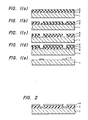
- FIGs 1(a)-1(e) An example of the steps of the lift-off process is illustrated in Figures 1(a)-1(e).
- the second photoresist film 3 is selectively exposed to light through a mask, and is developed to remove desired parts of the second photoresist film 3 as shown in Figure 1 (b). Since the developer used in this case does not dissolve the first photoresist film 2, only the desired parts of the second photoresist film are selectively removed.
- a material to form the microscopic pattern for example, aluminum is deposited on the whole surface by the vacuum evaporation or the like.
- the first photoresist film 2 is removed along with the second photoresist film 3 and the aluminum film 4 deposited thereon. Then, only the aluminum film 4 deposited directly on the substrate 1 remains, and the pattern of the aluminum is formed.
- the above lift-off process has hitherto used only positive photoresist materials.
- positive photoresist materials it is the parts of the photoresist film 3 which are to be removed which are exposed to light through a mask, so that they become more soluble than the unexposed parts.
- negative photoresist on the other hand, it is the parts of the film which are to remain which are exposed to light, so as to make them less soluble than the parts which are to be removed; but to date, such a negative photoresist has not been applied to a lift-off process.
- the lift-off process has the advantage of being capable of forming the microscopic pattern precisely, it is very complicated in practical use because it must stack and deposit the two sorts of photoresist films and carry out the developing time as described above. A simpler method has been eagerly desired.
- DE-A-2948324 there was disclosed a method of forming a microscopic pattern, which included the steps of depositing a film of photoresist on the surface on which the microscopic pattern was to be formed, the photoresist being a material containing benzene rings.
- the desired part of the photoresist material was then irradiated with short wavelength ultra-violet radiation (ultra-violet radiation whose wavelengths are approximately 200-320 nm shall be referred to as "short wavelength ultra-violet radiation" in this specification) to lower the solubility of the irradiated part.
- short wavelength ultra-violet radiation ultraviolet radiation
- the solvent system used was a mixture of n-heptane and xylene. This mixture will have the effect of also dissolving some of the exposed part of the photoresist and will therefore be unsatisfactory for producing precisely defined microscopic patterns.
- the present invention uses as developer an alkaline, aqueous solution to produce a photoresist pattern in the form of an inverted trapezoid. Furthermore, the method includes steps of
- the prior-art positive lift-off process has most commonly employed two kinds of photoresist or resin films or the like whose solubilities for a developer are different, and it has required such complicated steps as developing or dissolving them twice.
- the metal film 4 can be left only on the substrate 1, and the microscopic pattern made of the metal film 4 is formed.
- Our method uses as a negative photoresist a polymer which has a benzene ring or a photoresist which is formed by adding a certain aromatic azide to the polymer, whereby the photoresist pattern having the inverted-trapezoidal sectional shape is formed without using two kinds of photoresists, polymers or the like and by only one developing operation. This makes it very easy to perform the lift-off process very easily.
- a photoresist which contains a high polymer having a benzene ring for example, poly-p-vinyl phenol
- a photochemical reaction takes place to lower the solubility of the irradiated part, and the photoresist exhibits properties as a negative photoresist.
- the benzene reing which the photoresist contains absorbs the short-wavelength ultraviolet radiation very well.
- Figure 3 illustrates the relationships between the wavelength of ultraviolet radiation and the transmittance in the case where various photoresist films were irradiated with the ultraviolet radiation.
- curves a, b and c in Figure 3 all of photoresists AZ1350J and AZ2400 (both being trade names) which have benzene rings and a resist in which a sensitizer is added to poly-p-vinyl phenol absorb the short-wavelength ultraviolet radiation of wavelengths of and below approximately 320 nm very strongly.
- the photoresist film having the benzene ring is irradiated with the short-wavelength ultraviolet radiation, the attenuation of the irradiating radiation in the thickness direction is very great owing to the extraordinarily great absorption by the photoresist.
- the attenuation of the irradiating radiation in the thickness direction is very great owing to the extraordinarily great absorption by the photoresist.
- only a surface layer of the film is made perfectly insoluble, and a deeper part thereof is made less insoluble and comes to have a higher solubility.
- the surface layer of the irradiated area does not dissolve because it is perfectly insoluble. Since, however, the solubility gradually increases in the lower layer as described above, the unreacted part underlying the irradiated area is gradually removed with the proceeding of the developing.
- the photoresist pattern 5 having the inverted-trapezoidal sectional shape is formed as shown in Figure 2.
- the sectional shape of the photoresist pattern i.e., the length of the lower side of the photoresist pattern can be controlled as desired by the developing processing.
- the concentration of the developer when the concentration of the developer is raised, the lower layer is etched more and the length of the lower side decreases. If the concentration of the developer is held constant, the length of the lower side becomes smaller as the developing time is longer.
- the photoresist usable in our method needs to satisfy the two conditions that it contains the benzene ring and well absorbs the short-wavelength ultraviolet radiation of the wavelengths of and below approximately 320 nm, and that it can form a sharp microscopic pattern.
- a photoresist fulfilling such conditions there can be employed a polymer which has phenolic hydroxyl groups or a polymer to which a certain kind of aromatic azide is added.
- poly(vinyl phenol) for example, poly(vinyl phenol), addition condensation products between phenols or cresols and formaldehyde (the so-called novolac resins), bromides of poly(vinyl phenol), poly(vinyl hydroxybenzoate) or poly(vinyl hydroxybenzal), and poly(isopropenyl phenol).
- the aforecited azide needs to exhibit a great absorption for the short-wavelength ultraviolet radiation and to have no great absorption in a region of longer wavelengths.
- Azides which have a structure indicated by the following general formula (1) are preferable in practical use:
- A denotes a substituent unconjugate with the benzene rings, such as O, S, CH 2 , CH 2 CH 2 , S0 2 and S 2
- X denotes H or N 3
- Z denotes a substituent N 3 when X is H and a substituent H or CI when X is N 3 .
- the photoresists formed by combining the azides and the polymers there can be employed, for example, one in which the novolac resin of the type formed by copolymerization between phenol and m-cresol has 4,4'-diazidediphenylsulfide added thereto and is dissolved in methyl cellosolve acetate, and one in which poly-p-vinyl phenol and 3,3'-diazidediphenylsulfone are dissolved in methyl cellosolve acetate.
- AZ type photoresists in which naphthoquinone diazide etc. are added as sensitizers to a phenol novolac type polymer, such as AZ1350J and AZ2400 (both being trade names) produced by Shipley Inc., and commercially-available positive films which have compositions similar to those of the AZ type photoresists, for example, OFPR-77 (produced by Tokyo Ohkas trade name) and HPR-204 (produced by Hunt Chemical, trade name).
- alkaline aqueous solutions which are obtained by dissolving sodium hydroxide, potassium hydroxide, sodium phosphate, sodium silicate, tetramethylammonium hydroxide, etc. in water.
- liquid temperatures and developing times of developers are, of course, conspicuously different depending upon many factors including the kind of the developer used, the kind and film thickness of the photoresist, etc., they are approximately 10-40°C and approximately 10-600 seconds respectively.
- concentrations of the developers are approximately 0.1-10 weight-%.
- film thicknesses of the photoresists are different according to the kind of the photoresist used, the purpose, etc., they are selected in a range of approximately 0.5 ⁇ 3 pm.
- the quantities of exposure of the photoresist films are properly selected depending upon the kind of the photoresist and the sectional shape of the photoresist pattern to be formed.
- the AZ type photoresists produced by Shipley Inc., etc are used, they exhibit properties as positive photoresists with small quantities of exposure and cannot be used in this invention. Therefore, they must be subjected to an exposure of at least 300 mJ/cm 2 (a value at a wavelength of 254 nm, the same applying hereinbelow) so as to exhibit characteristics as negative photoresists.
- the quantity of exposure is selected from within a range of approximately 5-1,000 mJ/cm 2 , and the exposure time is approximately 5-500 seconds.
- the photoresist solution was applied on a silicon wafer by spin coating, to form a photoresist film 0.9 um thick.
- the photoresist film was exposed to light through a chromium mask formed on a quartz substrate.
- the light intensity at the wavelength of 254 nm was 5.5 mW/cm 2 , and the exposure time was 100 seconds.
- the photoresist film exposed to the light was developed with a 4% aqueous solution of tetramethylammonium hydroxide for 90 seconds. Then, striped photoresist patterns whose sectional shape was an inverted trapezoid with its upper side and its lower side being about 4.5 pm and 3.5 um long respectively were obtained.
- the photoresist solution was applied on a silicon wafer by spin coating, to form a photoresist film 0.9 ⁇ m thick.
- the photoresist film was exposed to light through a chromium mask formed on a quartz substrate.
- the light intensity at the wavelength of 254 nm was 5.5 mW/cm 2 , and the exposure time was 2 seconds.
- the photoresist film was developed with a 4% aqueous solution of tetramethylammonium hydroxide.
- Figures 4(a) and 4(b) are microphotographs of photoresist patterns taken with a scanning electron microscope after developing times of 50 seconds and 60 seconds, respectively.
- the width of the lower side is much smaller in the photoresist pattern obtained by developing for 60 seconds, than in the photoresist pattern obtained through the developing for 50 seconds.
- the width of the lower side of the resist pattern can be controlled by the developing time.
- a sectional shape which is the most suitable for performing the lift-off operation can be readily formed.
- various microscopic patterns such as interconnections can be formed at high precision by performing the lift-off operation very easily without using two kinds of photoresists or carrying out developing twice and with the same number of steps as in conventional photolithography.
Landscapes
- Physics & Mathematics (AREA)
- Spectroscopy & Molecular Physics (AREA)
- General Physics & Mathematics (AREA)
- Photosensitive Polymer And Photoresist Processing (AREA)
- Exposure Of Semiconductors, Excluding Electron Or Ion Beam Exposure (AREA)
- ing And Chemical Polishing (AREA)
- Weting (AREA)
Applications Claiming Priority (2)
| Application Number | Priority Date | Filing Date | Title |
|---|---|---|---|
| JP104990/80 | 1980-08-01 | ||
| JP10499080A JPS5730829A (en) | 1980-08-01 | 1980-08-01 | Micropattern formation method |
Publications (3)
| Publication Number | Publication Date |
|---|---|
| EP0045639A2 EP0045639A2 (en) | 1982-02-10 |
| EP0045639A3 EP0045639A3 (en) | 1982-08-04 |
| EP0045639B1 true EP0045639B1 (en) | 1985-10-23 |
Family
ID=14395526
Family Applications (1)
| Application Number | Title | Priority Date | Filing Date |
|---|---|---|---|
| EP81303514A Expired EP0045639B1 (en) | 1980-08-01 | 1981-07-31 | Method of forming a microscopic pattern |
Country Status (4)
| Country | Link |
|---|---|
| US (1) | US4536421A (ja) |
| EP (1) | EP0045639B1 (ja) |
| JP (1) | JPS5730829A (ja) |
| DE (1) | DE3172722D1 (ja) |
Families Citing this family (38)
| Publication number | Priority date | Publication date | Assignee | Title |
|---|---|---|---|---|
| JPS57160128A (en) * | 1981-03-30 | 1982-10-02 | Hitachi Ltd | Fine pattern forming method |
| JPS57204124A (en) * | 1981-06-10 | 1982-12-14 | Hitachi Ltd | Forming method for minute pattern |
| JPS5872139A (ja) * | 1981-10-26 | 1983-04-30 | Tokyo Ohka Kogyo Co Ltd | 感光性材料 |
| US4439516A (en) * | 1982-03-15 | 1984-03-27 | Shipley Company Inc. | High temperature positive diazo photoresist processing using polyvinyl phenol |
| JPS58203438A (ja) * | 1982-05-24 | 1983-11-26 | Hitachi Ltd | 微細パタ−ン形成方法 |
| JPS58205147A (ja) * | 1982-05-25 | 1983-11-30 | Sumitomo Chem Co Ltd | ポジ型フオトレジスト組成物 |
| DE3246106A1 (de) * | 1982-12-13 | 1984-06-14 | Hoechst Ag, 6230 Frankfurt | Lichtempfindliches gemisch, daraus hergestelltes lichtempfindliches kopiermaterial und verfahren zur herstellung einer druckform aus dem kopiermaterial |
| US4609615A (en) * | 1983-03-31 | 1986-09-02 | Oki Electric Industry Co., Ltd. | Process for forming pattern with negative resist using quinone diazide compound |
| EP0135900A3 (en) * | 1983-09-16 | 1986-06-11 | Olin Hunt Specialty Products, Inc. | Aqueous developable negative resist compositions |
| JPS60134236A (ja) * | 1983-12-23 | 1985-07-17 | Hitachi Ltd | 微細パタ−ン形成法 |
| JPH0622047B2 (ja) * | 1984-02-15 | 1994-03-23 | 株式会社日立製作所 | 磁気ヘツド |
| JPS61156044A (ja) * | 1984-12-27 | 1986-07-15 | Nec Corp | レジストステンシルマスクの製造方法 |
| JPS61275747A (ja) * | 1985-05-30 | 1986-12-05 | Nec Corp | ネガレジスト材料 |
| US4670297A (en) * | 1985-06-21 | 1987-06-02 | Raytheon Company | Evaporated thick metal and airbridge interconnects and method of manufacture |
| US4897338A (en) * | 1987-08-03 | 1990-01-30 | Allied-Signal Inc. | Method for the manufacture of multilayer printed circuit boards |
| DE3800617A1 (de) * | 1988-01-12 | 1989-07-20 | Hoechst Ag | Elektrophotographisches aufzeichnungsmaterial |
| JPH0285857A (ja) * | 1988-09-22 | 1990-03-27 | Toshiba Corp | 感光性樹脂組成物 |
| JP2538081B2 (ja) * | 1988-11-28 | 1996-09-25 | 松下電子工業株式会社 | 現像液及びパタ―ン形成方法 |
| US5486449A (en) * | 1989-02-07 | 1996-01-23 | Rohm Co., Ltd. | Photomask, photoresist and photolithography for a monolithic IC |
| US5126232A (en) * | 1989-05-26 | 1992-06-30 | Seagate Technology, Inc. | Pole design for thin film magnetic heads |
| US5156936A (en) * | 1989-09-19 | 1992-10-20 | U.S. Philips Corporation | Contact device for the photocathode of photoelectric tubes and manufacturing method |
| US5221596A (en) * | 1991-09-03 | 1993-06-22 | Motorola, Inc. | Method of forming a retrograde photoresist profile |
| US5281447A (en) * | 1991-10-25 | 1994-01-25 | International Business Machines Corporation | Patterned deposition of metals via photochemical decomposition of metal-oxalate complexes |
| US6344234B1 (en) * | 1995-06-07 | 2002-02-05 | International Business Machines Corportion | Method for forming reflowed solder ball with low melting point metal cap |
| SE9502258D0 (sv) * | 1995-06-21 | 1995-06-21 | Pharmacia Biotech Ab | Method for the manufacture of a membrane-containing microstructure |
| US5786028A (en) * | 1996-09-05 | 1998-07-28 | Cantwell; Jay S. | Masking tape and method |
| US6220333B1 (en) | 1998-11-06 | 2001-04-24 | Jay S. Cantwell | Bar code stencil and method of use |
| JP2003241183A (ja) * | 2002-02-13 | 2003-08-27 | Koninkl Philips Electronics Nv | 拡散反射構造体を用いた液晶表示装置及びその製造方法 |
| JP2004193332A (ja) * | 2002-12-11 | 2004-07-08 | Oki Electric Ind Co Ltd | 成膜方法 |
| JP4513965B2 (ja) * | 2004-03-31 | 2010-07-28 | 日本ゼオン株式会社 | 感放射線性樹脂組成物 |
| TWI314249B (en) | 2004-03-31 | 2009-09-01 | Zeon Corp | Radiation-sensitive resin composition |
| US9142533B2 (en) * | 2010-05-20 | 2015-09-22 | Taiwan Semiconductor Manufacturing Company, Ltd. | Substrate interconnections having different sizes |
| US9425136B2 (en) | 2012-04-17 | 2016-08-23 | Taiwan Semiconductor Manufacturing Company, Ltd. | Conical-shaped or tier-shaped pillar connections |
| US9299674B2 (en) | 2012-04-18 | 2016-03-29 | Taiwan Semiconductor Manufacturing Company, Ltd. | Bump-on-trace interconnect |
| CN103426978B (zh) * | 2012-05-17 | 2016-09-07 | 泰州畅瑞照明有限公司 | Led芯片的制造方法 |
| US9111817B2 (en) | 2012-09-18 | 2015-08-18 | Taiwan Semiconductor Manufacturing Company, Ltd. | Bump structure and method of forming same |
| CN104797086A (zh) * | 2014-01-17 | 2015-07-22 | 冠捷投资有限公司 | 于基材上形成线路图形的方法 |
| CN112992660B (zh) * | 2021-05-10 | 2021-08-03 | 度亘激光技术(苏州)有限公司 | 半导体结构形成方法 |
Citations (1)
| Publication number | Priority date | Publication date | Assignee | Title |
|---|---|---|---|---|
| EP0001429A1 (de) * | 1977-09-29 | 1979-04-18 | International Business Machines Corporation | Verfahren zur Herstellung von Dünnfilmmustern unter Anwendung der Abhebetechnologie |
Family Cites Families (12)
| Publication number | Priority date | Publication date | Assignee | Title |
|---|---|---|---|---|
| DE1956282A1 (de) * | 1969-11-08 | 1971-05-13 | Agfa Gevaert Ag | Lichtvernetzbare Schichten |
| GB1375461A (ja) * | 1972-05-05 | 1974-11-27 | ||
| JPS5388728A (en) * | 1977-01-14 | 1978-08-04 | Toshiba Corp | Method of forming pattern |
| JPS5934293B2 (ja) * | 1977-04-20 | 1984-08-21 | 王子製紙株式会社 | 感光性組成物 |
| JPS5472976A (en) * | 1977-11-22 | 1979-06-11 | Fujitsu Ltd | Pattern forming method |
| US4211834A (en) * | 1977-12-30 | 1980-07-08 | International Business Machines Corporation | Method of using a o-quinone diazide sensitized phenol-formaldehyde resist as a deep ultraviolet light exposure mask |
| US4212935A (en) * | 1978-02-24 | 1980-07-15 | International Business Machines Corporation | Method of modifying the development profile of photoresists |
| DE2948324C2 (de) * | 1978-12-01 | 1993-01-14 | Hitachi, Ltd., Tokio/Tokyo | Lichtempfindliches Gemisch, enthaltend eine Bisazidverbindung, und Verfahren zur Bildung von Mustern |
| JPS5820420B2 (ja) * | 1978-12-15 | 1983-04-22 | 富士通株式会社 | パタ−ン形成方法 |
| JPS5595945A (en) * | 1979-01-12 | 1980-07-21 | Nec Corp | Production of negative type resist image |
| JPS55156941A (en) * | 1979-05-24 | 1980-12-06 | Tokyo Ohka Kogyo Co Ltd | Micropattern forming method |
| JPS628777A (ja) * | 1985-07-03 | 1987-01-16 | 株式会社 タカラ | 変形玩具 |
-
1980
- 1980-08-01 JP JP10499080A patent/JPS5730829A/ja active Pending
-
1981
- 1981-07-30 US US06/288,481 patent/US4536421A/en not_active Expired - Fee Related
- 1981-07-31 DE DE8181303514T patent/DE3172722D1/de not_active Expired
- 1981-07-31 EP EP81303514A patent/EP0045639B1/en not_active Expired
Patent Citations (1)
| Publication number | Priority date | Publication date | Assignee | Title |
|---|---|---|---|---|
| EP0001429A1 (de) * | 1977-09-29 | 1979-04-18 | International Business Machines Corporation | Verfahren zur Herstellung von Dünnfilmmustern unter Anwendung der Abhebetechnologie |
Also Published As
| Publication number | Publication date |
|---|---|
| JPS5730829A (en) | 1982-02-19 |
| DE3172722D1 (en) | 1985-11-28 |
| US4536421A (en) | 1985-08-20 |
| EP0045639A2 (en) | 1982-02-10 |
| EP0045639A3 (en) | 1982-08-04 |
Similar Documents
| Publication | Publication Date | Title |
|---|---|---|
| EP0045639B1 (en) | Method of forming a microscopic pattern | |
| US4609615A (en) | Process for forming pattern with negative resist using quinone diazide compound | |
| JPH0220869A (ja) | 乾式現像用レジスト | |
| US4943511A (en) | High sensitivity mid and deep UV resist | |
| EP0040535B1 (en) | Method of forming a microscopic pattern, and a photoresist | |
| JPH0210350A (ja) | ポジ型フォトレジスト | |
| JPS62270952A (ja) | 二層フオトレジストの現像 | |
| EP0327991A2 (en) | Radiation sensitive recording material comprising a polysulfone barrier layer | |
| KR100477401B1 (ko) | 이온 교환에 의해 유기 극성 용제를 함유하는 포토레지스트 조성물내의 금속 이온 오염물을 감소시키는 방법 | |
| US4464458A (en) | Process for forming resist masks utilizing O-quinone diazide and pyrene | |
| EP0336605B1 (en) | High sensitivity mid and deep uv resist | |
| GB2079481A (en) | Method for the formation of surface relief patterns using deep ultraviolet radiation exposure of resist composition | |
| US5719004A (en) | Positive photoresist composition containing a 2,4-dinitro-1-naphthol | |
| US4801518A (en) | Method of forming a photoresist pattern | |
| JPS6037548A (ja) | 照射線反応ネガレジストの形成方法 | |
| US5240807A (en) | Photoresist article having a portable, conformable, built-on mask | |
| US5702862A (en) | Positive photoresist coating solution comprising a mixed solvent of propylene glycol monopropyl ether and 2-heptanone | |
| US3992208A (en) | Photo-sensitive etchant and method for forming metal image using same | |
| US5238773A (en) | Alkaline developable photoresist composition containing radiation sensitive organosilicon compound with quinone diazide terminal groups | |
| JPH09211868A (ja) | T字形状断面を有するホトレジストパターンの製造方法 | |
| EP0225464A2 (en) | Composite resist structures | |
| US5306595A (en) | Composition containing naphthoquinone diazide sulfonic acid mixed esters and radiation-sensitive recording material prepared therewith | |
| JPS58203438A (ja) | 微細パタ−ン形成方法 | |
| US6841338B2 (en) | Photoresist composition and method of forming a photoresist pattern with a controlled remnant ratio | |
| JPS58214149A (ja) | 微細パタ−ン形成方法 |
Legal Events
| Date | Code | Title | Description |
|---|---|---|---|
| PUAI | Public reference made under article 153(3) epc to a published international application that has entered the european phase |
Free format text: ORIGINAL CODE: 0009012 |
|
| 17P | Request for examination filed |
Effective date: 19810910 |
|
| AK | Designated contracting states |
Designated state(s): DE FR GB NL |
|
| RBV | Designated contracting states (corrected) |
Designated state(s): CH DE FR GB IT LI LU NL SE |
|
| PUAL | Search report despatched |
Free format text: ORIGINAL CODE: 0009013 |
|
| AK | Designated contracting states |
Designated state(s): DE FR GB NL |
|
| GRAA | (expected) grant |
Free format text: ORIGINAL CODE: 0009210 |
|
| AK | Designated contracting states |
Designated state(s): DE FR GB NL |
|
| REF | Corresponds to: |
Ref document number: 3172722 Country of ref document: DE Date of ref document: 19851128 |
|
| ET | Fr: translation filed | ||
| PLBE | No opposition filed within time limit |
Free format text: ORIGINAL CODE: 0009261 |
|
| STAA | Information on the status of an ep patent application or granted ep patent |
Free format text: STATUS: NO OPPOSITION FILED WITHIN TIME LIMIT |
|
| 26N | No opposition filed | ||
| PGFP | Annual fee paid to national office [announced via postgrant information from national office to epo] |
Ref country code: FR Payment date: 19940712 Year of fee payment: 14 |
|
| PGFP | Annual fee paid to national office [announced via postgrant information from national office to epo] |
Ref country code: GB Payment date: 19940721 Year of fee payment: 14 |
|
| PGFP | Annual fee paid to national office [announced via postgrant information from national office to epo] |
Ref country code: NL Payment date: 19940731 Year of fee payment: 14 |
|
| PGFP | Annual fee paid to national office [announced via postgrant information from national office to epo] |
Ref country code: DE Payment date: 19940926 Year of fee payment: 14 |
|
| PG25 | Lapsed in a contracting state [announced via postgrant information from national office to epo] |
Ref country code: GB Effective date: 19950731 |
|
| PG25 | Lapsed in a contracting state [announced via postgrant information from national office to epo] |
Ref country code: NL Effective date: 19960201 |
|
| GBPC | Gb: european patent ceased through non-payment of renewal fee |
Effective date: 19950731 |
|
| NLV4 | Nl: lapsed or anulled due to non-payment of the annual fee |
Effective date: 19960201 |
|
| PG25 | Lapsed in a contracting state [announced via postgrant information from national office to epo] |
Ref country code: DE Effective date: 19960402 |
|
| PG25 | Lapsed in a contracting state [announced via postgrant information from national office to epo] |
Ref country code: FR Effective date: 19960430 |
|
| REG | Reference to a national code |
Ref country code: FR Ref legal event code: ST |
|
| REG | Reference to a national code |
Ref country code: FR Ref legal event code: ST |
|
| REG | Reference to a national code |
Ref country code: FR Ref legal event code: ST |