EP0032788B2 - Procédé pour le dépôt de revêtements par décharge lumineuse - Google Patents
Procédé pour le dépôt de revêtements par décharge lumineuse Download PDFInfo
- Publication number
- EP0032788B2 EP0032788B2 EP81300053A EP81300053A EP0032788B2 EP 0032788 B2 EP0032788 B2 EP 0032788B2 EP 81300053 A EP81300053 A EP 81300053A EP 81300053 A EP81300053 A EP 81300053A EP 0032788 B2 EP0032788 B2 EP 0032788B2
- Authority
- EP
- European Patent Office
- Prior art keywords
- cathode
- substrate
- carbon
- plasma
- gas
- Prior art date
- Legal status (The legal status is an assumption and is not a legal conclusion. Google has not performed a legal analysis and makes no representation as to the accuracy of the status listed.)
- Expired
Links
- 238000000576 coating method Methods 0.000 title claims description 27
- 238000000151 deposition Methods 0.000 title claims description 18
- 238000000034 method Methods 0.000 title claims description 18
- 239000000758 substrate Substances 0.000 claims description 50
- 229910052799 carbon Inorganic materials 0.000 claims description 25
- OKTJSMMVPCPJKN-UHFFFAOYSA-N Carbon Chemical compound [C] OKTJSMMVPCPJKN-UHFFFAOYSA-N 0.000 claims description 23
- 239000011248 coating agent Substances 0.000 claims description 18
- 229910052732 germanium Inorganic materials 0.000 claims description 11
- GNPVGFCGXDBREM-UHFFFAOYSA-N germanium atom Chemical compound [Ge] GNPVGFCGXDBREM-UHFFFAOYSA-N 0.000 claims description 10
- 229910052710 silicon Inorganic materials 0.000 claims description 10
- 239000010703 silicon Substances 0.000 claims description 10
- 150000002500 ions Chemical class 0.000 claims description 6
- 239000004215 Carbon black (E152) Substances 0.000 claims description 5
- BLRPTPMANUNPDV-UHFFFAOYSA-N Silane Chemical compound [SiH4] BLRPTPMANUNPDV-UHFFFAOYSA-N 0.000 claims description 5
- 229910000078 germane Inorganic materials 0.000 claims description 5
- 229930195733 hydrocarbon Natural products 0.000 claims description 5
- 150000002430 hydrocarbons Chemical class 0.000 claims description 5
- 229910000077 silane Inorganic materials 0.000 claims description 5
- 125000004432 carbon atom Chemical group C* 0.000 claims description 3
- 239000007789 gas Substances 0.000 description 14
- 230000008021 deposition Effects 0.000 description 12
- XKRFYHLGVUSROY-UHFFFAOYSA-N argon Substances [Ar] XKRFYHLGVUSROY-UHFFFAOYSA-N 0.000 description 10
- XUIMIQQOPSSXEZ-UHFFFAOYSA-N Silicon Chemical compound [Si] XUIMIQQOPSSXEZ-UHFFFAOYSA-N 0.000 description 8
- 229910052786 argon Inorganic materials 0.000 description 6
- 239000000463 material Substances 0.000 description 6
- -1 Argon ions Chemical class 0.000 description 5
- 239000001273 butane Substances 0.000 description 5
- 229910021385 hard carbon Inorganic materials 0.000 description 5
- IJDNQMDRQITEOD-UHFFFAOYSA-N n-butane Chemical compound CCCC IJDNQMDRQITEOD-UHFFFAOYSA-N 0.000 description 5
- OFBQJSOFQDEBGM-UHFFFAOYSA-N n-pentane Natural products CCCCC OFBQJSOFQDEBGM-UHFFFAOYSA-N 0.000 description 5
- 238000004140 cleaning Methods 0.000 description 4
- 238000004544 sputter deposition Methods 0.000 description 4
- 239000004411 aluminium Substances 0.000 description 3
- XAGFODPZIPBFFR-UHFFFAOYSA-N aluminium Chemical compound [Al] XAGFODPZIPBFFR-UHFFFAOYSA-N 0.000 description 3
- 229910052782 aluminium Inorganic materials 0.000 description 3
- XYFCBTPGUUZFHI-UHFFFAOYSA-N Phosphine Chemical compound P XYFCBTPGUUZFHI-UHFFFAOYSA-N 0.000 description 2
- ATUOYWHBWRKTHZ-UHFFFAOYSA-N Propane Chemical compound CCC ATUOYWHBWRKTHZ-UHFFFAOYSA-N 0.000 description 2
- UORVGPXVDQYIDP-UHFFFAOYSA-N borane Chemical compound B UORVGPXVDQYIDP-UHFFFAOYSA-N 0.000 description 2
- 239000003990 capacitor Substances 0.000 description 2
- 239000010408 film Substances 0.000 description 2
- 238000007733 ion plating Methods 0.000 description 2
- 239000002245 particle Substances 0.000 description 2
- PFNQVRZLDWYSCW-UHFFFAOYSA-N (fluoren-9-ylideneamino) n-naphthalen-1-ylcarbamate Chemical compound C12=CC=CC=C2C2=CC=CC=C2C1=NOC(=O)NC1=CC=CC2=CC=CC=C12 PFNQVRZLDWYSCW-UHFFFAOYSA-N 0.000 description 1
- LFQSCWFLJHTTHZ-UHFFFAOYSA-N Ethanol Chemical compound CCO LFQSCWFLJHTTHZ-UHFFFAOYSA-N 0.000 description 1
- 239000005083 Zinc sulfide Substances 0.000 description 1
- 125000004429 atom Chemical group 0.000 description 1
- 229910000085 borane Inorganic materials 0.000 description 1
- XFWJKVMFIVXPKK-UHFFFAOYSA-N calcium;oxido(oxo)alumane Chemical compound [Ca+2].[O-][Al]=O.[O-][Al]=O XFWJKVMFIVXPKK-UHFFFAOYSA-N 0.000 description 1
- 229910021386 carbon form Inorganic materials 0.000 description 1
- 239000004020 conductor Substances 0.000 description 1
- 239000000356 contaminant Substances 0.000 description 1
- 239000000498 cooling water Substances 0.000 description 1
- 239000011521 glass Substances 0.000 description 1
- 239000012535 impurity Substances 0.000 description 1
- 239000012212 insulator Substances 0.000 description 1
- 230000004048 modification Effects 0.000 description 1
- 238000012986 modification Methods 0.000 description 1
- 230000007935 neutral effect Effects 0.000 description 1
- 229910000073 phosphorus hydride Inorganic materials 0.000 description 1
- 239000001294 propane Substances 0.000 description 1
- 230000005855 radiation Effects 0.000 description 1
- 239000004065 semiconductor Substances 0.000 description 1
- 239000007787 solid Substances 0.000 description 1
- 239000002904 solvent Substances 0.000 description 1
- 229910001220 stainless steel Inorganic materials 0.000 description 1
- 239000010935 stainless steel Substances 0.000 description 1
- 239000013077 target material Substances 0.000 description 1
- 239000010409 thin film Substances 0.000 description 1
- XLYOFNOQVPJJNP-UHFFFAOYSA-N water Substances O XLYOFNOQVPJJNP-UHFFFAOYSA-N 0.000 description 1
- DRDVZXDWVBGGMH-UHFFFAOYSA-N zinc;sulfide Chemical compound [S-2].[Zn+2] DRDVZXDWVBGGMH-UHFFFAOYSA-N 0.000 description 1
Images
Classifications
-
- C—CHEMISTRY; METALLURGY
- C23—COATING METALLIC MATERIAL; COATING MATERIAL WITH METALLIC MATERIAL; CHEMICAL SURFACE TREATMENT; DIFFUSION TREATMENT OF METALLIC MATERIAL; COATING BY VACUUM EVAPORATION, BY SPUTTERING, BY ION IMPLANTATION OR BY CHEMICAL VAPOUR DEPOSITION, IN GENERAL; INHIBITING CORROSION OF METALLIC MATERIAL OR INCRUSTATION IN GENERAL
- C23C—COATING METALLIC MATERIAL; COATING MATERIAL WITH METALLIC MATERIAL; SURFACE TREATMENT OF METALLIC MATERIAL BY DIFFUSION INTO THE SURFACE, BY CHEMICAL CONVERSION OR SUBSTITUTION; COATING BY VACUUM EVAPORATION, BY SPUTTERING, BY ION IMPLANTATION OR BY CHEMICAL VAPOUR DEPOSITION, IN GENERAL
- C23C14/00—Coating by vacuum evaporation, by sputtering or by ion implantation of the coating forming material
- C23C14/22—Coating by vacuum evaporation, by sputtering or by ion implantation of the coating forming material characterised by the process of coating
- C23C14/34—Sputtering
- C23C14/3435—Applying energy to the substrate during sputtering
- C23C14/345—Applying energy to the substrate during sputtering using substrate bias
-
- C—CHEMISTRY; METALLURGY
- C23—COATING METALLIC MATERIAL; COATING MATERIAL WITH METALLIC MATERIAL; CHEMICAL SURFACE TREATMENT; DIFFUSION TREATMENT OF METALLIC MATERIAL; COATING BY VACUUM EVAPORATION, BY SPUTTERING, BY ION IMPLANTATION OR BY CHEMICAL VAPOUR DEPOSITION, IN GENERAL; INHIBITING CORROSION OF METALLIC MATERIAL OR INCRUSTATION IN GENERAL
- C23C—COATING METALLIC MATERIAL; COATING MATERIAL WITH METALLIC MATERIAL; SURFACE TREATMENT OF METALLIC MATERIAL BY DIFFUSION INTO THE SURFACE, BY CHEMICAL CONVERSION OR SUBSTITUTION; COATING BY VACUUM EVAPORATION, BY SPUTTERING, BY ION IMPLANTATION OR BY CHEMICAL VAPOUR DEPOSITION, IN GENERAL
- C23C14/00—Coating by vacuum evaporation, by sputtering or by ion implantation of the coating forming material
- C23C14/22—Coating by vacuum evaporation, by sputtering or by ion implantation of the coating forming material characterised by the process of coating
- C23C14/34—Sputtering
-
- C—CHEMISTRY; METALLURGY
- C23—COATING METALLIC MATERIAL; COATING MATERIAL WITH METALLIC MATERIAL; CHEMICAL SURFACE TREATMENT; DIFFUSION TREATMENT OF METALLIC MATERIAL; COATING BY VACUUM EVAPORATION, BY SPUTTERING, BY ION IMPLANTATION OR BY CHEMICAL VAPOUR DEPOSITION, IN GENERAL; INHIBITING CORROSION OF METALLIC MATERIAL OR INCRUSTATION IN GENERAL
- C23C—COATING METALLIC MATERIAL; COATING MATERIAL WITH METALLIC MATERIAL; SURFACE TREATMENT OF METALLIC MATERIAL BY DIFFUSION INTO THE SURFACE, BY CHEMICAL CONVERSION OR SUBSTITUTION; COATING BY VACUUM EVAPORATION, BY SPUTTERING, BY ION IMPLANTATION OR BY CHEMICAL VAPOUR DEPOSITION, IN GENERAL
- C23C16/00—Chemical coating by decomposition of gaseous compounds, without leaving reaction products of surface material in the coating, i.e. chemical vapour deposition [CVD] processes
- C23C16/44—Chemical coating by decomposition of gaseous compounds, without leaving reaction products of surface material in the coating, i.e. chemical vapour deposition [CVD] processes characterised by the method of coating
- C23C16/458—Chemical coating by decomposition of gaseous compounds, without leaving reaction products of surface material in the coating, i.e. chemical vapour deposition [CVD] processes characterised by the method of coating characterised by the method used for supporting substrates in the reaction chamber
-
- C—CHEMISTRY; METALLURGY
- C23—COATING METALLIC MATERIAL; COATING MATERIAL WITH METALLIC MATERIAL; CHEMICAL SURFACE TREATMENT; DIFFUSION TREATMENT OF METALLIC MATERIAL; COATING BY VACUUM EVAPORATION, BY SPUTTERING, BY ION IMPLANTATION OR BY CHEMICAL VAPOUR DEPOSITION, IN GENERAL; INHIBITING CORROSION OF METALLIC MATERIAL OR INCRUSTATION IN GENERAL
- C23C—COATING METALLIC MATERIAL; COATING MATERIAL WITH METALLIC MATERIAL; SURFACE TREATMENT OF METALLIC MATERIAL BY DIFFUSION INTO THE SURFACE, BY CHEMICAL CONVERSION OR SUBSTITUTION; COATING BY VACUUM EVAPORATION, BY SPUTTERING, BY ION IMPLANTATION OR BY CHEMICAL VAPOUR DEPOSITION, IN GENERAL
- C23C16/00—Chemical coating by decomposition of gaseous compounds, without leaving reaction products of surface material in the coating, i.e. chemical vapour deposition [CVD] processes
- C23C16/44—Chemical coating by decomposition of gaseous compounds, without leaving reaction products of surface material in the coating, i.e. chemical vapour deposition [CVD] processes characterised by the method of coating
- C23C16/50—Chemical coating by decomposition of gaseous compounds, without leaving reaction products of surface material in the coating, i.e. chemical vapour deposition [CVD] processes characterised by the method of coating using electric discharges
-
- H—ELECTRICITY
- H01—ELECTRIC ELEMENTS
- H01L—SEMICONDUCTOR DEVICES NOT COVERED BY CLASS H10
- H01L31/00—Semiconductor devices sensitive to infrared radiation, light, electromagnetic radiation of shorter wavelength or corpuscular radiation and specially adapted either for the conversion of the energy of such radiation into electrical energy or for the control of electrical energy by such radiation; Processes or apparatus specially adapted for the manufacture or treatment thereof or of parts thereof; Details thereof
- H01L31/18—Processes or apparatus specially adapted for the manufacture or treatment of these devices or of parts thereof
- H01L31/20—Processes or apparatus specially adapted for the manufacture or treatment of these devices or of parts thereof such devices or parts thereof comprising amorphous semiconductor materials
- H01L31/202—Processes or apparatus specially adapted for the manufacture or treatment of these devices or of parts thereof such devices or parts thereof comprising amorphous semiconductor materials including only elements of Group IV of the Periodic System
-
- Y—GENERAL TAGGING OF NEW TECHNOLOGICAL DEVELOPMENTS; GENERAL TAGGING OF CROSS-SECTIONAL TECHNOLOGIES SPANNING OVER SEVERAL SECTIONS OF THE IPC; TECHNICAL SUBJECTS COVERED BY FORMER USPC CROSS-REFERENCE ART COLLECTIONS [XRACs] AND DIGESTS
- Y02—TECHNOLOGIES OR APPLICATIONS FOR MITIGATION OR ADAPTATION AGAINST CLIMATE CHANGE
- Y02E—REDUCTION OF GREENHOUSE GAS [GHG] EMISSIONS, RELATED TO ENERGY GENERATION, TRANSMISSION OR DISTRIBUTION
- Y02E10/00—Energy generation through renewable energy sources
- Y02E10/50—Photovoltaic [PV] energy
-
- Y—GENERAL TAGGING OF NEW TECHNOLOGICAL DEVELOPMENTS; GENERAL TAGGING OF CROSS-SECTIONAL TECHNOLOGIES SPANNING OVER SEVERAL SECTIONS OF THE IPC; TECHNICAL SUBJECTS COVERED BY FORMER USPC CROSS-REFERENCE ART COLLECTIONS [XRACs] AND DIGESTS
- Y02—TECHNOLOGIES OR APPLICATIONS FOR MITIGATION OR ADAPTATION AGAINST CLIMATE CHANGE
- Y02P—CLIMATE CHANGE MITIGATION TECHNOLOGIES IN THE PRODUCTION OR PROCESSING OF GOODS
- Y02P70/00—Climate change mitigation technologies in the production process for final industrial or consumer products
- Y02P70/50—Manufacturing or production processes characterised by the final manufactured product
Definitions
- This invention concerns a method for depositing coatings in a glow discharge plasma.
- Carbon coatings are useful on for example germanium lenses used in infra red thermal ima- gers since the carbon coatings are very hard, wear-resistant and substantially transparent to infra red radiation. Both silicon and germanium are transparent to infra red and are useful in various infra red equipments.
- a substrate may be suspended above a cathode target of the coating material in a vacuum.
- Argon ions are caused to strike the target thereby knocking off small particles of the target material which adhere to the substrate.
- Such a technique is known as sputtering.
- Carbon can be sputtered but the coating formed is graphitic not diamond-like.
- Coatings may be grown in a plasma.
- a substrate may be used as a cathode in a D.C. or R.F. excited hydrocarbon plasma. Carbon ions are attracted to strike the substrate and form a carbon layer which for appropriate temperature and pressure conditions, is diamond-like.
- silicon and germanium may be respectively grown from a silane and germane plasma.
- Amorphous layers of silicon have been grown for use as solar cells by controlling doping impurities in the plasma. This control of doping allows p-n junctions and p-i-n junctions to be formed by deposition in a glow discharge.
- a disadvantage with the prior art glow discharge deposition is that in order to achieve reasonable deposition rates high potentials have to be applied or developed at the cathode, so that the substrate is subjected to high energy incident particles. This tends to affect the stress in the coating and increases the back sputtering rate. In some cases this prevents deposition of a layer at all.
- the generation of ions and the deposition of a coating are controlled independently.
- a method of depositing an infra red transparent coating comprises the steps of admitting a hydro carbon gas into a chamber, providing a plasma of the gas between an anode and cathode in the chamber by application of an electrical potential between the anode and cathode, arranging the surface of a substrate to be coated to face the cathode in a position spaced from and parallel thereto, controlling the substrate temperature independently of the plasma temperature by a heater and cooler, controlling the substrate potential independently of the potential on the cathode at a value of -200V D.C.
- Apparatus for depositing a coating on a substrate by the method of this invention comprises a vacuum tight chamber, a pump for providing a vacuum within the chamber, means for introducing a gas of material to be deposited as a coating into the chamber, means for applying a controllable voltage between an anode and a cathode within the chamber to provide a plasma of the gas in the chamber, means for supporting a substrate with a surface to be coated facing the cathode in a position spaced from and parallel thereto, the electrical potential of the substrate being controllable independently of the potential of the cathode, means for controlling the temperature of the substrate independently of the plasma temperature, the arrangement being capable of providing conditions of vacuum and voltage on the cathode such that, in operation, positive ions of material to be deposited are attracted to and strike the cathode where they are neutralised to form atoms of the coating material which leave the cathode to form the required coating on the substrate.
- the method and apparatus may include a bias voltage supply to the substrate for preliminary cleaning and for use during deposition of carbon to affect an ion plating enhancement of the deposition.
- the gas admitted to the chamber may be a hydro carbon (e.g. propane, butane, etc.) to form a hard carbon coating; silane to form a thin silicon bonding layer, or germane to form a thin germanium bonding layer.
- a hydro carbon e.g. propane, butane, etc.
- silane to form a thin silicon bonding layer
- germane to form a thin germanium bonding layer.
- the method of this invention separates the generation of ions of carbon, silicon, germanium and the deposition onto the substrate. Also the substrate temperature and potential is independent of the temperature and potential involved in the generation of the ions.
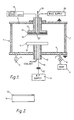
- a substrate 16 to be coated is held in a substrate mounting 17 which is insulated from the top plate 3.
- the distance between the cathode plate 11 and substrate 16 is typically 7 cm.
- Inside the substrate mounting 17 is a heater/cooler 18 connected to a heater/cooler supply 19 outside the chamber 1.
- the substrate 16 nay have a bias voltage applied thereto from a bias voltage supply 20.
- a sheathed thermocoupler 21 passes inside a tube 22 in the mounting 17 to measure substrate 16 temperature.
- the RF supply 14 is replaced by a D.C. supply and the capacitor 15 removed.
- Operation to carbon coat a substrate of electrically conducting (e.g. resistivity 5 - 20 ohm cm) doped germanium is as follows.
- the substrate 16 is mounted on the mounting 17 and cleaned in the usual manner e.g. by wiping with a solvent such as alcohol.
- the apparatus of Figure 1 is assembled and the chamber 1 evacuated by the pump 9 to less than 1.3 x 10 . 3 Pa (10 , 5 Torr) to remove contaminants.
- Argon gas is admitted through the valve 6 and pipe 5 to a pressure of about 1.33 Pa (10- 2 Torr.) on an air calibrated gauge and the substrate 16 heated to about 200°C.
- the plasma is generated in argon by energising the cathode 10 whilst a bias voltage of about -200 volts D.C. is applied to the substrate 16 from the supply 20. This provides bombardment of the substrate with argon ions thereby cleaning the substrate surface to be coated. About 2 minutes of cleaning is adequate. The cleaning bias voltage is then removed.
- argon is then removed from the chamber 1 by the pump 9 and a hydro-carbon gas, e.g. butane, is admitted to the chamber 1 through the inlet pipe 5 to a pressure of 0.93 to 1.3 Pa (0.7 to 1 x 10' Torr) on the air calibrated gauge.
- a hydro-carbon gas e.g. butane
- a bias voltage of about -200 volts D.C. is applied to the heated substrate 16 and the RF supply 14 to the cathode 11 is switched on.
- the RF is 1 kVolt at 13 MHz, and at 200 watts power.
- the butane gas becomes ionised; positively charged carbon ions strike the cathode 11 where some stick but most leave as neutral carbon atoms and strike the substrate 16.
- the result of the bias voltage on the substrate is to increase bonding between substrate and carbon by the process of ion plating. After an initial amount of carbon has been deposited the bias voltage is gradually reduced to around 0 from - 200 volts D.C.
- the substrate is coated to a thickness of about 1 11m with a hard carbon coating 23 ( Figure 2).
- the apparatus is then switched off and allowed to cool.
- the above process of depositing hard carbon using an RF supply can also be carried out using a D.C. (direct current) supply.
- the cathode supply is at about -1 kVolt.
- Electrically insulating substrates nay also be coated with hard carbon coatings.
- hard carbon coatings For example calcium aluminate, zinc sulphide, and zinc sele- nide may be coated.
- a thin bonding layer of silicon or germanium may be deposited on e.g. aluminium or stainless steel, or glass, substrates prior to carbon coating.
- Such bonding layers may be deposited by sputtering off a silicon or germanium target in a well known matter. Alternatively the bonding layers may be deposited by glow discharge using a gas of silane or germane instead of butane in the illustrated apparatus. Deposition of the carbon layer follows deposition of the bonding layer. For some substrate materials an initial bonding layer of oxide may be necessary under the silicon or germanium layer.
Landscapes
- Chemical & Material Sciences (AREA)
- Engineering & Computer Science (AREA)
- Chemical Kinetics & Catalysis (AREA)
- Materials Engineering (AREA)
- Mechanical Engineering (AREA)
- Metallurgy (AREA)
- Organic Chemistry (AREA)
- General Chemical & Material Sciences (AREA)
- Physics & Mathematics (AREA)
- Manufacturing & Machinery (AREA)
- Plasma & Fusion (AREA)
- Condensed Matter Physics & Semiconductors (AREA)
- Electromagnetism (AREA)
- General Physics & Mathematics (AREA)
- Computer Hardware Design (AREA)
- Microelectronics & Electronic Packaging (AREA)
- Power Engineering (AREA)
- Chemical Vapour Deposition (AREA)
- Carbon And Carbon Compounds (AREA)
- Photovoltaic Devices (AREA)
- Physical Vapour Deposition (AREA)
Claims (3)
Applications Claiming Priority (2)
| Application Number | Priority Date | Filing Date | Title |
|---|---|---|---|
| GB8001383 | 1980-01-16 | ||
| GB8001383 | 1980-01-16 |
Publications (3)
| Publication Number | Publication Date |
|---|---|
| EP0032788A1 EP0032788A1 (fr) | 1981-07-29 |
| EP0032788B1 EP0032788B1 (fr) | 1984-12-19 |
| EP0032788B2 true EP0032788B2 (fr) | 1989-12-06 |
Family
ID=10510662
Family Applications (1)
| Application Number | Title | Priority Date | Filing Date |
|---|---|---|---|
| EP81300053A Expired EP0032788B2 (fr) | 1980-01-16 | 1981-01-07 | Procédé pour le dépôt de revêtements par décharge lumineuse |
Country Status (5)
| Country | Link |
|---|---|
| US (1) | US4394400A (fr) |
| EP (1) | EP0032788B2 (fr) |
| JP (1) | JPS56146876A (fr) |
| DE (1) | DE3167761D1 (fr) |
| GB (1) | GB2069008B (fr) |
Families Citing this family (57)
| Publication number | Priority date | Publication date | Assignee | Title |
|---|---|---|---|---|
| GB7910479D0 (en) * | 1979-03-26 | 1999-12-01 | Secr Defence | Camouflage |
| EP0049032B1 (fr) * | 1980-08-21 | 1986-09-17 | National Research Development Corporation | Revêtement de matériaux isolants à l'aide d'une décharge luminescente |
| US4504519A (en) * | 1981-10-21 | 1985-03-12 | Rca Corporation | Diamond-like film and process for producing same |
| FR2514743B1 (fr) * | 1981-10-21 | 1986-05-09 | Rca Corp | Pellicule amorphe a base de carbone, du type diamant, et son procede de fabrication |
| JPS58117868A (ja) * | 1981-12-28 | 1983-07-13 | Toshiba Corp | 皮膜形成装置 |
| DE3206421A1 (de) * | 1982-02-23 | 1983-09-01 | Siemens AG, 1000 Berlin und 8000 München | Verfahren zum herstellen von schichten aus hochschmelzenden metallen bzw. metallverbindungen durch abscheidung aus der dampfphase |
| GB2119278B (en) * | 1982-04-13 | 1987-04-15 | Michael Paul Neary | Improvements in or relating to a chemical method |
| GB2164581A (en) * | 1982-04-13 | 1986-03-26 | Michael Paul Neary | Chemical method |
| GB2122224B (en) * | 1982-06-23 | 1986-06-11 | Atomic Energy Authority Uk | Ion beam carbon layers |
| JPS5930709A (ja) * | 1982-08-13 | 1984-02-18 | Toa Nenryo Kogyo Kk | 炭素膜及び/又は炭素粒子の製造方法 |
| JPS5966343A (ja) * | 1982-10-08 | 1984-04-14 | バ−・アンド・ストラウド・リミテツド | 光学的被膜の製造方法 |
| EP0106638A1 (fr) * | 1982-10-12 | 1984-04-25 | National Research Development Corporation | Procédé et appareil pour la croissance des matières au moyen d'une décharge luminescente |
| US4704339A (en) * | 1982-10-12 | 1987-11-03 | The Secretary Of State For Defence In Her Britannic Majesty's Government Of The United Kingdom Of Great Britain And Northern Ireland | Infra-red transparent optical components |
| GB2165266B (en) * | 1982-10-12 | 1987-09-23 | Nat Res Dev | Infra red transparent optical components |
| EP0106637B1 (fr) * | 1982-10-12 | 1988-02-17 | National Research Development Corporation | Eléments optiques transparents aux rayons infrarouges |
| JPH0674504B2 (ja) * | 1983-07-21 | 1994-09-21 | キヤノン株式会社 | 堆積膜の製造方法 |
| DE3335623A1 (de) * | 1983-09-30 | 1985-04-11 | Siemens AG, 1000 Berlin und 8000 München | Verfahren zur herstellung einer kohlenstoff enthaltenden schicht, kohlenstoff enthaltende schicht, verwendung einer kohlenstoff enthaltenden schicht und vorrichtung zur durchfuehrung eines verfahrens zur herstellung einer kohlenstoff enthaltenden schicht |
| CA1235087A (fr) * | 1983-11-28 | 1988-04-12 | Akio Hiraki | Couche mince diamantine, et sa fabrication |
| GB2291888B (en) * | 1984-06-08 | 1996-06-26 | Barr & Stroud Ltd | Optical coating |
| US4607193A (en) * | 1984-10-10 | 1986-08-19 | The United States Of America As Represented By The Administrator Of The National Aeronautics And Space Administration | Textured carbon surfaces on copper by sputtering |
| GB8431422D0 (en) * | 1984-12-13 | 1985-01-23 | Standard Telephones Cables Ltd | Plasma reactor vessel |
| GB8504458D0 (en) * | 1985-02-21 | 1985-03-27 | Gen Eng Radcliffe Ltd | Producing multi-layered coatings |
| JPS61196538A (ja) * | 1985-02-27 | 1986-08-30 | Hitachi Ltd | 真空処理方法及び装置 |
| GB2175016B (en) * | 1985-05-11 | 1990-01-24 | Barr & Stroud Ltd | Optical coating |
| DE3664791D1 (en) * | 1985-06-05 | 1989-09-07 | Plessey Overseas | Methods of depositing germanium carbide |
| EP0209972A1 (fr) * | 1985-06-05 | 1987-01-28 | Plessey Overseas Limited | Procédé pour le dépôt d'un carbure de germanium hydrogéné |
| US4626448A (en) * | 1985-07-18 | 1986-12-02 | The United States Of America As Represented By The United States Department Of Energy | Plasma deposition of amorphous metal alloys |
| DE3538261A1 (de) * | 1985-10-28 | 1987-04-30 | Battelle Institut E V | Gegeneinander abdichtende ventilelemente fuer mischarmaturen |
| US4910153A (en) * | 1986-02-18 | 1990-03-20 | Solarex Corporation | Deposition feedstock and dopant materials useful in the fabrication of hydrogenated amorphous silicon alloys for photovoltaic devices and other semiconductor devices |
| US4690830A (en) * | 1986-02-18 | 1987-09-01 | Solarex Corporation | Activation by dehydrogenation or dehalogenation of deposition feedstock and dopant materials useful in the fabrication of hydrogenated amorphous silicon alloys for photovoltaic devices and other semiconductor devices |
| US4756964A (en) * | 1986-09-29 | 1988-07-12 | The Dow Chemical Company | Barrier films having an amorphous carbon coating and methods of making |
| US4902531A (en) * | 1986-10-30 | 1990-02-20 | Nihon Shinku Gijutsu Kabushiki Kaisha | Vacuum processing method and apparatus |
| JPH0672306B2 (ja) * | 1987-04-27 | 1994-09-14 | 株式会社半導体エネルギー研究所 | プラズマ処理装置およびプラズマ処理方法 |
| GB8713922D0 (en) * | 1987-06-15 | 1994-06-22 | Secr Defence | Infra red transparent windows |
| US4911795A (en) * | 1987-08-14 | 1990-03-27 | Morton Thiokol, Inc. | Method of preserving a composite material cased solid propellant rocket motor |
| JPH03163820A (ja) * | 1989-11-22 | 1991-07-15 | Tokai Univ | ダイヤモンドn型半導体およびダイヤモンドp―n接合ダイオードの製造方法 |
| EP0447155B1 (fr) * | 1990-03-12 | 1995-07-26 | Ngk Insulators, Ltd. | Calorifères pour pastilles semi-conductrices pour un appareil produisant des semi-conducteurs, unités de chauffage utilisant de tels calorifères, et production de calorifères |
| GB9019219D0 (en) * | 1990-09-01 | 1990-10-17 | Atomic Energy Authority Uk | Diamond-like carbon coatings |
| US5397428A (en) * | 1991-12-20 | 1995-03-14 | The University Of North Carolina At Chapel Hill | Nucleation enhancement for chemical vapor deposition of diamond |
| BE1006967A3 (fr) * | 1993-04-16 | 1995-02-07 | Cockerill Rech & Dev | Procede pour la formation d'un revetement sur un substrat par pulverisation cathodique reactive. |
| NZ277879A (en) * | 1994-02-01 | 1998-03-25 | Howmedica | Fermoral stem prosthesis, formed from biocompatible material and having a coated surface of specified material |
| US5688557A (en) * | 1995-06-07 | 1997-11-18 | Lemelson; Jerome H. | Method of depositing synthetic diamond coatings with intermediates bonding layers |
| US5951773A (en) * | 1996-03-18 | 1999-09-14 | Hyundai Electronics Industries Co., Ltd. | Inductively coupled plasma chemical vapor deposition apparatus |
| US6320261B1 (en) | 1998-04-21 | 2001-11-20 | Micron Technology, Inc. | High aspect ratio metallization structures for shallow junction devices, and methods of forming the same |
| US6121134A (en) * | 1998-04-21 | 2000-09-19 | Micron Technology, Inc. | High aspect ratio metallization structures and processes for fabricating the same |
| AU2002235146A1 (en) | 2000-11-30 | 2002-06-11 | North Carolina State University | Non-thermionic sputter material transport device, methods of use, and materials produced thereby |
| KR100831751B1 (ko) | 2000-11-30 | 2008-05-23 | 노쓰 캐롤라이나 스테이트 유니버시티 | M'n 물의 제조 방법 및 장치 |
| US8220489B2 (en) | 2002-12-18 | 2012-07-17 | Vapor Technologies Inc. | Faucet with wear-resistant valve component |
| US6904935B2 (en) | 2002-12-18 | 2005-06-14 | Masco Corporation Of Indiana | Valve component with multiple surface layers |
| US7866343B2 (en) | 2002-12-18 | 2011-01-11 | Masco Corporation Of Indiana | Faucet |
| US8555921B2 (en) | 2002-12-18 | 2013-10-15 | Vapor Technologies Inc. | Faucet component with coating |
| US7866342B2 (en) | 2002-12-18 | 2011-01-11 | Vapor Technologies, Inc. | Valve component for faucet |
| JP4660241B2 (ja) * | 2005-03-25 | 2011-03-30 | 株式会社昭和真空 | スパッタ装置 |
| US20070026205A1 (en) | 2005-08-01 | 2007-02-01 | Vapor Technologies Inc. | Article having patterned decorative coating |
| US20090008577A1 (en) * | 2007-07-07 | 2009-01-08 | Varian Semiconductor Equipment Associates, Inc. | Conformal Doping Using High Neutral Density Plasma Implant |
| CN102426790B (zh) * | 2011-08-21 | 2015-02-04 | 苏以捷 | 平面交叉路口通行控制系统和方法 |
| JP2018104249A (ja) * | 2016-12-28 | 2018-07-05 | 国立大学法人京都大学 | 被膜付き化合物および被膜付き化合物の製造方法 |
Family Cites Families (13)
| Publication number | Priority date | Publication date | Assignee | Title |
|---|---|---|---|---|
| GB1104935A (en) * | 1964-05-08 | 1968-03-06 | Standard Telephones Cables Ltd | Improvements in or relating to a method of forming a layer of an inorganic compound |
| US3472751A (en) * | 1965-06-16 | 1969-10-14 | Ion Physics Corp | Method and apparatus for forming deposits on a substrate by cathode sputtering using a focussed ion beam |
| US3419487A (en) * | 1966-01-24 | 1968-12-31 | Dow Corning | Method of growing thin film semiconductors using an electron beam |
| DE1621358A1 (de) * | 1966-11-08 | 1971-04-29 | Texas Instruments Inc | Verfahren zur Aufbringung duenner Filme aus dielektrischem Material auf ein Substrat |
| US3471396A (en) * | 1967-04-10 | 1969-10-07 | Ibm | R.f. cathodic sputtering apparatus having an electrically conductive housing |
| US3650737A (en) * | 1968-03-25 | 1972-03-21 | Ibm | Imaging method using photoconductive element having a protective coating |
| US3600218A (en) * | 1968-05-15 | 1971-08-17 | Ibm | Method for depositing insulating films of silicon nitride and aluminum nitride |
| JPS5123393B2 (fr) * | 1972-10-03 | 1976-07-16 | ||
| IT1203089B (it) * | 1976-03-03 | 1989-02-15 | Int Plasma Corp | Procedimento ed apparecchiatura per eseguire reazioni chimiche nella regione della scarica luminescente di un plasma |
| DE2624005C2 (de) * | 1976-05-28 | 1982-04-08 | Siemens AG, 1000 Berlin und 8000 München | Verfahren und Vorrichtung zum Aufbringen von dünnen Schichten auf ein Substrat nach dem "Ion-plating"-Verfahren. |
| GB1582231A (en) * | 1976-08-13 | 1981-01-07 | Nat Res Dev | Application of a layer of carbonaceous material to a surface |
| JPS5419662A (en) * | 1977-07-15 | 1979-02-14 | Hitachi Ltd | Forming method of plasma cvd film |
| JPS5468169A (en) * | 1977-11-11 | 1979-06-01 | Hitachi Ltd | Plasma processor of capacitor type |
-
1981
- 1981-01-07 GB GB8100335A patent/GB2069008B/en not_active Expired
- 1981-01-07 DE DE8181300053T patent/DE3167761D1/de not_active Expired
- 1981-01-07 EP EP81300053A patent/EP0032788B2/fr not_active Expired
- 1981-01-13 US US06/224,825 patent/US4394400A/en not_active Expired - Lifetime
- 1981-01-16 JP JP393381A patent/JPS56146876A/ja active Granted
Also Published As
| Publication number | Publication date |
|---|---|
| JPS56146876A (en) | 1981-11-14 |
| JPH036223B2 (fr) | 1991-01-29 |
| DE3167761D1 (en) | 1985-01-31 |
| GB2069008B (en) | 1984-09-12 |
| US4394400A (en) | 1983-07-19 |
| EP0032788A1 (fr) | 1981-07-29 |
| EP0032788B1 (fr) | 1984-12-19 |
| GB2069008A (en) | 1981-08-19 |
Similar Documents
| Publication | Publication Date | Title |
|---|---|---|
| EP0032788B2 (fr) | Procédé pour le dépôt de revêtements par décharge lumineuse | |
| EP0049032B1 (fr) | Revêtement de matériaux isolants à l'aide d'une décharge luminescente | |
| US4412903A (en) | Coating infra red transparent semiconductor material | |
| US4728406A (en) | Method for plasma - coating a semiconductor body | |
| EP0106637B1 (fr) | Eléments optiques transparents aux rayons infrarouges | |
| EP0768388B1 (fr) | Procédé et appareil de production d'un film à base de carbone amorphe | |
| US4704339A (en) | Infra-red transparent optical components | |
| AU4768793A (en) | Microwave energized deposition process with substrate temperature control | |
| US4933203A (en) | Process for depositing amorphous hydrogenated silicon in a plasma chamber | |
| GB2083841A (en) | Glow discharge coating | |
| EP0659905B1 (fr) | Appareil CVD assisté par plasma capable de supprimer la génération de poudre de polysilane | |
| Boxman et al. | Filtered vacuum arc deposition of semiconductor thin films | |
| GB2148947A (en) | Method of depositing an amorphous semiconductor layer from a glow discharge | |
| GB2082562A (en) | Coating germanium or silica with carbon | |
| EP0106638A1 (fr) | Procédé et appareil pour la croissance des matières au moyen d'une décharge luminescente | |
| US20010025601A1 (en) | Apparatus and method for forming a deposited film by means of plasma CVD | |
| US6495000B1 (en) | System and method for DC sputtering oxide films with a finned anode | |
| CN115029669B (zh) | 一种采用液态金属高功率脉冲磁控溅射提高沉积效率的方法 | |
| GB2240114A (en) | Film nucleation process for growing diamond film | |
| JP3513206B2 (ja) | 堆積膜形成方法及び堆積膜形成装置 | |
| JP3639453B2 (ja) | 化合物半導体薄膜の製造装置およびこれを用いた化合物半導体薄膜の製造方法 | |
| Felmetsger et al. | Dual cathode DC–RF and MF–RF coupled S-Guns for reactive sputtering | |
| Petrov et al. | Effect of ion bombardment during growth on the electrical resistivity of magnetron-sputtered carbon films | |
| US5753379A (en) | Protective coatings for optical components | |
| KR102595151B1 (ko) | 연료전지용 금속분리판 및 그 제조방법 |
Legal Events
| Date | Code | Title | Description |
|---|---|---|---|
| PUAI | Public reference made under article 153(3) epc to a published international application that has entered the european phase |
Free format text: ORIGINAL CODE: 0009012 |
|
| AK | Designated contracting states |
Designated state(s): DE FR GB NL |
|
| 17P | Request for examination filed |
Effective date: 19820114 |
|
| GRAA | (expected) grant |
Free format text: ORIGINAL CODE: 0009210 |
|
| AK | Designated contracting states |
Designated state(s): DE FR GB NL |
|
| REF | Corresponds to: |
Ref document number: 3167761 Country of ref document: DE Date of ref document: 19850131 |
|
| ET | Fr: translation filed | ||
| PLBI | Opposition filed |
Free format text: ORIGINAL CODE: 0009260 |
|
| PLBI | Opposition filed |
Free format text: ORIGINAL CODE: 0009260 |
|
| 26 | Opposition filed |
Opponent name: STANDARD ELEKTRIK LORENZ AG Effective date: 19850827 |
|
| 26 | Opposition filed |
Opponent name: LEYBOLD - HERAEUS GMBH Effective date: 19850916 |
|
| NLR1 | Nl: opposition has been filed with the epo |
Opponent name: STANDARD ELEKTRIK LORENZ AG |
|
| NLR1 | Nl: opposition has been filed with the epo |
Opponent name: LEYBOLD - HERAEUS GMBH |
|
| PUAH | Patent maintained in amended form |
Free format text: ORIGINAL CODE: 0009272 |
|
| STAA | Information on the status of an ep patent application or granted ep patent |
Free format text: STATUS: PATENT MAINTAINED AS AMENDED |
|
| 27A | Patent maintained in amended form |
Effective date: 19891206 |
|
| AK | Designated contracting states |
Kind code of ref document: B2 Designated state(s): DE FR GB NL |
|
| ET1 | Fr: translation filed ** revision of the translation of the patent or the claims | ||
| ET3 | Fr: translation filed ** decision concerning opposition | ||
| NLR2 | Nl: decision of opposition | ||
| NLR3 | Nl: receipt of modified translations in the netherlands language after an opposition procedure | ||
| REG | Reference to a national code |
Ref country code: GB Ref legal event code: 732 |
|
| REG | Reference to a national code |
Ref country code: FR Ref legal event code: TP |
|
| NLS | Nl: assignments of ep-patents |
Owner name: BRITISH TECHNOLOGY GROUP LTD TE LONDEN, GROOT-BRIT |
|
| PGFP | Annual fee paid to national office [announced via postgrant information from national office to epo] |
Ref country code: GB Payment date: 19991027 Year of fee payment: 20 |
|
| PGFP | Annual fee paid to national office [announced via postgrant information from national office to epo] |
Ref country code: FR Payment date: 19991103 Year of fee payment: 20 |
|
| PGFP | Annual fee paid to national office [announced via postgrant information from national office to epo] |
Ref country code: DE Payment date: 19991104 Year of fee payment: 20 |
|
| PGFP | Annual fee paid to national office [announced via postgrant information from national office to epo] |
Ref country code: NL Payment date: 19991108 Year of fee payment: 20 |
|
| PG25 | Lapsed in a contracting state [announced via postgrant information from national office to epo] |
Ref country code: GB Free format text: LAPSE BECAUSE OF EXPIRATION OF PROTECTION Effective date: 20010106 |
|
| PG25 | Lapsed in a contracting state [announced via postgrant information from national office to epo] |
Ref country code: NL Free format text: LAPSE BECAUSE OF EXPIRATION OF PROTECTION Effective date: 20010107 |
|
| REG | Reference to a national code |
Ref country code: GB Ref legal event code: PE20 Effective date: 20010106 |
|
| NLV7 | Nl: ceased due to reaching the maximum lifetime of a patent |
Effective date: 20010107 |