EP0025347A2 - Dispositifs semiconducteurs comportant des fusibles - Google Patents
Dispositifs semiconducteurs comportant des fusibles Download PDFInfo
- Publication number
- EP0025347A2 EP0025347A2 EP80303113A EP80303113A EP0025347A2 EP 0025347 A2 EP0025347 A2 EP 0025347A2 EP 80303113 A EP80303113 A EP 80303113A EP 80303113 A EP80303113 A EP 80303113A EP 0025347 A2 EP0025347 A2 EP 0025347A2
- Authority
- EP
- European Patent Office
- Prior art keywords
- fuses
- protecting layer
- fuse
- semiconductor device
- centre portions
- Prior art date
- Legal status (The legal status is an assumption and is not a legal conclusion. Google has not performed a legal analysis and makes no representation as to the accuracy of the status listed.)
- Granted
Links
- 239000004065 semiconductor Substances 0.000 title claims abstract description 21
- 238000007664 blowing Methods 0.000 claims abstract description 3
- VYPSYNLAJGMNEJ-UHFFFAOYSA-N Silicium dioxide Chemical compound O=[Si]=O VYPSYNLAJGMNEJ-UHFFFAOYSA-N 0.000 claims description 12
- 239000005360 phosphosilicate glass Substances 0.000 claims description 7
- 229910052581 Si3N4 Inorganic materials 0.000 claims description 6
- HQVNEWCFYHHQES-UHFFFAOYSA-N silicon nitride Chemical compound N12[Si]34N5[Si]62N3[Si]51N64 HQVNEWCFYHHQES-UHFFFAOYSA-N 0.000 claims description 6
- 235000012239 silicon dioxide Nutrition 0.000 claims description 5
- 239000000377 silicon dioxide Substances 0.000 claims description 5
- 239000000463 material Substances 0.000 claims description 4
- 239000004642 Polyimide Substances 0.000 claims description 2
- 229920001721 polyimide Polymers 0.000 claims description 2
- 230000002950 deficient Effects 0.000 description 8
- 238000001259 photo etching Methods 0.000 description 5
- 239000004020 conductor Substances 0.000 description 4
- XUIMIQQOPSSXEZ-UHFFFAOYSA-N Silicon Chemical compound [Si] XUIMIQQOPSSXEZ-UHFFFAOYSA-N 0.000 description 3
- 230000015572 biosynthetic process Effects 0.000 description 3
- 238000005229 chemical vapour deposition Methods 0.000 description 3
- 229910021420 polycrystalline silicon Inorganic materials 0.000 description 3
- 229920005591 polysilicon Polymers 0.000 description 3
- 229910052710 silicon Inorganic materials 0.000 description 3
- 239000010703 silicon Substances 0.000 description 3
- 239000000758 substrate Substances 0.000 description 3
- 230000007547 defect Effects 0.000 description 2
- 239000011159 matrix material Substances 0.000 description 2
- 229910001120 nichrome Inorganic materials 0.000 description 2
- MAKDTFFYCIMFQP-UHFFFAOYSA-N titanium tungsten Chemical compound [Ti].[W] MAKDTFFYCIMFQP-UHFFFAOYSA-N 0.000 description 2
- 238000007740 vapor deposition Methods 0.000 description 2
- ZXEYZECDXFPJRJ-UHFFFAOYSA-N $l^{3}-silane;platinum Chemical compound [SiH3].[Pt] ZXEYZECDXFPJRJ-UHFFFAOYSA-N 0.000 description 1
- 239000004411 aluminium Substances 0.000 description 1
- 229910052782 aluminium Inorganic materials 0.000 description 1
- XAGFODPZIPBFFR-UHFFFAOYSA-N aluminium Chemical compound [Al] XAGFODPZIPBFFR-UHFFFAOYSA-N 0.000 description 1
- 230000000052 comparative effect Effects 0.000 description 1
- 238000005520 cutting process Methods 0.000 description 1
- 238000004519 manufacturing process Methods 0.000 description 1
- 229910044991 metal oxide Inorganic materials 0.000 description 1
- 150000004706 metal oxides Chemical class 0.000 description 1
- 238000000034 method Methods 0.000 description 1
- 230000003647 oxidation Effects 0.000 description 1
- 238000007254 oxidation reaction Methods 0.000 description 1
- 230000001590 oxidative effect Effects 0.000 description 1
- 238000004544 sputter deposition Methods 0.000 description 1
- 239000007858 starting material Substances 0.000 description 1
Images

Classifications
-
- G—PHYSICS
- G11—INFORMATION STORAGE
- G11C—STATIC STORES
- G11C17/00—Read-only memories programmable only once; Semi-permanent stores, e.g. manually-replaceable information cards
- G11C17/14—Read-only memories programmable only once; Semi-permanent stores, e.g. manually-replaceable information cards in which contents are determined by selectively establishing, breaking or modifying connecting links by permanently altering the state of coupling elements, e.g. PROM
- G11C17/16—Read-only memories programmable only once; Semi-permanent stores, e.g. manually-replaceable information cards in which contents are determined by selectively establishing, breaking or modifying connecting links by permanently altering the state of coupling elements, e.g. PROM using electrically-fusible links
-
- H—ELECTRICITY
- H01—ELECTRIC ELEMENTS
- H01L—SEMICONDUCTOR DEVICES NOT COVERED BY CLASS H10
- H01L23/00—Details of semiconductor or other solid state devices
- H01L23/52—Arrangements for conducting electric current within the device in operation from one component to another, i.e. interconnections, e.g. wires, lead frames
- H01L23/522—Arrangements for conducting electric current within the device in operation from one component to another, i.e. interconnections, e.g. wires, lead frames including external interconnections consisting of a multilayer structure of conductive and insulating layers inseparably formed on the semiconductor body
- H01L23/525—Arrangements for conducting electric current within the device in operation from one component to another, i.e. interconnections, e.g. wires, lead frames including external interconnections consisting of a multilayer structure of conductive and insulating layers inseparably formed on the semiconductor body with adaptable interconnections
- H01L23/5256—Arrangements for conducting electric current within the device in operation from one component to another, i.e. interconnections, e.g. wires, lead frames including external interconnections consisting of a multilayer structure of conductive and insulating layers inseparably formed on the semiconductor body with adaptable interconnections comprising fuses, i.e. connections having their state changed from conductive to non-conductive
-
- H—ELECTRICITY
- H01—ELECTRIC ELEMENTS
- H01L—SEMICONDUCTOR DEVICES NOT COVERED BY CLASS H10
- H01L23/00—Details of semiconductor or other solid state devices
- H01L23/58—Structural electrical arrangements for semiconductor devices not otherwise provided for, e.g. in combination with batteries
- H01L23/62—Protection against overvoltage, e.g. fuses, shunts
-
- H—ELECTRICITY
- H01—ELECTRIC ELEMENTS
- H01L—SEMICONDUCTOR DEVICES NOT COVERED BY CLASS H10
- H01L2924/00—Indexing scheme for arrangements or methods for connecting or disconnecting semiconductor or solid-state bodies as covered by H01L24/00
- H01L2924/0001—Technical content checked by a classifier
- H01L2924/0002—Not covered by any one of groups H01L24/00, H01L24/00 and H01L2224/00
Definitions
- the present invention relates to semiconductor devices having fuses and, more particularly, to memory devices having spare (i.e. redundant) memory cells, and fuse-link programmable read-only memory (PROM) devices.
- spare i.e. redundant
- PROM fuse-link programmable read-only memory
- a semiconductor memory is organized as a matrix of horizontal or row lines and vertical or column lines. At each intersection of the matrix a memory cell is provided which is able to store one bit of information. If at least one defect, e.g. a defective memory cell, occurs in a memory device, the device should be abandoned. However, if the number of the defects is small, the bad memory device can be changed into a good memory device by using a redundancy technique. It is possible to remarkably increase the production yield by providing redundant (i.e. spare) row and column lines in the memory device. The spare row lines and spare column lines which form spare memory cells are built into the memory device while.it is being produced. When, for example, a row line of a defective memory cell (i.e.
- the defective row line is eliminated and a spare row line is substituted in its place.
- the defective row line is cut off from the regular row decoder thereof and, simultaneously, the spare row decoder of the spare row line is formed to respond to the same address as that of the defective row line to be replaced.
- the spare row decoder behaves exactly like the regular row decoder.
- the above-mentioned cutting off of the defective row line and formation of the spare row decoder can be carried out by blowing fuses provided between the regular row recoder and the row line and within the spare row recoder.
- a defective column line can be eliminated and a spare column line can be substituted in its place.
- fuses are formed in every row line, every column line, every spare row decoder and every spare column decoder of a semiconductor memory device.
- PROM fuse-link-programmable read--only memory
- a fuse element comprising the above-mentioned fuses of the semiconductor memory device having redundant memory cells and of the fuse-link PROM has a structure as illustrated in Fig. 1.
- the fuse element 1 of Fig. 1 is produced in the following manner.
- the starting material is a semiconductor substrate (e.g. silicon wafer) 2.
- An isolating layer (e.g. silicon dioxide layer) 3 is formed on the semiconductor substrate 2 by chemical vapor deposition or thermal oxidation of silicon.
- Fuse material e.g.
- polysilicon nichrome (Ni-Cr), titanium-tungsten (Ti-W) or platinum silicide (PtSi) is deposited on the isolating layer 3 by vapor deposition or sputtering and, then, is patterned by photoetching to form a fuse 4 having a so-called bow-tie shape which consists of two relatively large rectangular portions and a belt shaped portion connecting the two rectangular portions.
- An insulating layer 5 of silicon dioxide (Si0 2 ), silicon nitride (SiN 4 ) or phospho-silicate glass (PSG) is formed on the fuse 4 and the isolating layer 3 by chemical vapor deposition and, then, is selectively etched to open two windows for electrical contact on the fuse 4 by photoetching. Then, a conductor material (e.g. aluminium) is formed by vapor deposition and is selectively etched to form predetermined conductor lines 6 by photoetching.
- a protecting layer 7 of silicon dioxide, silicon nitride or phospho-silicate glass is formed on the conductor lines 6-and the insulating layer 5.
- Fusing of the fuse 4 is performed by passing a fusing current through the fuse 4 via the conductor lines 6.
- the fusing current is limited to a value of current which is allowed to pass through a metal oxide semiconductor (MOS) transistor or a bipolar transistor in a memory device.
- MOS metal oxide semiconductor
- a fuse can not be blown by passing a predetermined fusing current and/or that a small bridge is formed between separated portions of the blown fuse, and therefore, fuse-reliability is low.
- An object of the present invention is to increase the fuse-reliability in a semiconductor device, by providing improved fuses which blow easily and surely on the application of a fusing current.
- a semiconductor device has fuses coated with a protecting layer and is characterized in that narrow centre portions of the fuses are exposed through a window formed in the said protecting layer.
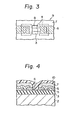
- FIG. 2 and 3 there is illustrated a fuse element 9 improved in accordance with the present invention.
- Reference numerals 2 through 7 in Figures 2 and 3 represent the same parts as those represented by the reference numerals 2 through 7 in Figure 1.
- a window 8 is opened by photoetching to expose a narrow centre portion of the fuse 4 as illustrated in Figs. 2 and 3.
- the fuse 4 has a bow-tie shape as illustrated in Fig. 3, so that the narrow center portion exposed within the window 8 of the fuse 4 can be easily and surely blown by passing a fusing current through the fuse 4.
- a gap between separated portions of the fuse 4 generated by fusing is wider than that between separated portions of a fuse which is completely coated with a protecting layer being generated by fusing.
- the narrow center portion of each blown and unblown fuse in a semiconductor device is exposed within windows formed in the protecting layer 7.
- an additional protecting layer 10 of phosphosilicate glass, silicon nitride or polyimide subsequent to the fusing operation, so as to plug up the window 8, as illustrated in Fig. 4.
- the blown fuses and unblown fuses in the semiconductor device are coated with the additional protecting layer 10.
- Bow-tie shaped fuses of polysilicon were formed by chemical vapor deposition on a silicon dioxide (Si0 2 ) layer which was formed by thermally oxidizing a silicon single crystalline substrate.
- Each of the fuses had a thickness of 0.3 microns.
- a narrow center portion of the fuse had a width of 2.5 microns and a length of 7 microns.
- rectangular windows of 5 microns by 10 microns were formed in the protecting layer on the narrow center portions of the fuses by photoetching.
- the fuses were blown by passing a fusing current through the fuses. The peak value of the fusing current was in the range of from 50 to 60 milliamperes.
- the above--mentioned polysilicon fuses were blown by passing a fusing current prior to the opening of the windows.
- the peak value of the fusing current was in the range of from 70 to 80 milliamperes.
- fused gaps between separated portions of the fuses with windows were wider than those of separated portions of the fuses without windows.
Landscapes
- Physics & Mathematics (AREA)
- Condensed Matter Physics & Semiconductors (AREA)
- General Physics & Mathematics (AREA)
- Engineering & Computer Science (AREA)
- Computer Hardware Design (AREA)
- Microelectronics & Electronic Packaging (AREA)
- Power Engineering (AREA)
- Design And Manufacture Of Integrated Circuits (AREA)
- Lead Frames For Integrated Circuits (AREA)
Applications Claiming Priority (2)
| Application Number | Priority Date | Filing Date | Title |
|---|---|---|---|
| JP122908/79 | 1979-09-05 | ||
| JP1979122908U JPS5847596Y2 (ja) | 1979-09-05 | 1979-09-05 | 半導体装置 |
Publications (3)
| Publication Number | Publication Date |
|---|---|
| EP0025347A2 true EP0025347A2 (fr) | 1981-03-18 |
| EP0025347A3 EP0025347A3 (en) | 1982-12-29 |
| EP0025347B1 EP0025347B1 (fr) | 1987-04-29 |
Family
ID=14847583
Family Applications (1)
| Application Number | Title | Priority Date | Filing Date |
|---|---|---|---|
| EP80303113A Expired EP0025347B1 (fr) | 1979-09-05 | 1980-09-04 | Dispositifs semiconducteurs comportant des fusibles |
Country Status (4)
| Country | Link |
|---|---|
| US (1) | US4413272A (fr) |
| EP (1) | EP0025347B1 (fr) |
| JP (1) | JPS5847596Y2 (fr) |
| DE (1) | DE3071961D1 (fr) |
Cited By (14)
| Publication number | Priority date | Publication date | Assignee | Title |
|---|---|---|---|---|
| EP0089814A2 (fr) * | 1982-03-18 | 1983-09-28 | Fujitsu Limited | Procédé pour la fabrication de connexions fusibles dans un dispositif semi-conducteur |
| EP0090565A2 (fr) * | 1982-03-30 | 1983-10-05 | Fujitsu Limited | Procédé pour couper sélectivement une couche électroconductrice par irradiation avec un faisceau d'énergie |
| EP0128675A1 (fr) * | 1983-05-16 | 1984-12-19 | Fujitsu Limited | Procédé de fabrication d'un circuit intégré à métallisation multicouche avec un fusible et une ouverture pour le fusible |
| GB2153590A (en) * | 1984-02-01 | 1985-08-21 | Ramesh Chandra Varshney | Matrix of functional circuits on a semiconductor wafer |
| EP0162145A1 (fr) * | 1984-02-23 | 1985-11-27 | Kabushiki Kaisha Toshiba | Procédé de faire fondre une connection fusible en utilisant un faisceau laser |
| FR2569054A1 (fr) * | 1984-08-10 | 1986-02-14 | Eurotechnique Sa | Dispositif de neutralisation de l'acces a une zone a proteger d'un circuit integre |
| FR2590421A1 (fr) * | 1985-11-15 | 1987-05-22 | Thomson Csf | Dispositif de protection contre la foudre par resistance fusible et serigraphiee, procede de fabrication, et application aux calculateurs embarques a bord d'aeronefs |
| EP0269775A1 (fr) * | 1986-12-02 | 1988-06-08 | Thomson-Csf | Dispositif de protection contre la foudre par résistance fusible et sérigraphiée, procédé de fabrication, et application aux calculateurs embarqués à bord d'aéronefs |
| US4795720A (en) * | 1984-07-11 | 1989-01-03 | Hitachi, Ltd. | Method for producing semiconductor devices and cutting fuses |
| GB2237446A (en) * | 1989-10-24 | 1991-05-01 | Seikosha Kk | Fuse for a semi-conductor device |
| EP0531128A1 (fr) * | 1991-09-04 | 1993-03-10 | Fujitsu Limited | Dispositif semi-conducteur comprenant un fusible |
| US5300456A (en) * | 1993-06-17 | 1994-04-05 | Texas Instruments Incorporated | Metal-to-metal antifuse structure |
| US5412593A (en) * | 1994-01-12 | 1995-05-02 | Texas Instruments Incorporated | Fuse and antifuse reprogrammable link for integrated circuits |
| EP0735583A2 (fr) * | 1995-03-30 | 1996-10-02 | Texas Instruments Incorporated | Circuits intégrés à semi-conducteur |
Families Citing this family (54)
| Publication number | Priority date | Publication date | Assignee | Title |
|---|---|---|---|---|
| US4585490A (en) * | 1981-12-07 | 1986-04-29 | Massachusetts Institute Of Technology | Method of making a conductive path in multi-layer metal structures by low power laser beam |
| US4810663A (en) * | 1981-12-07 | 1989-03-07 | Massachusetts Institute Of Technology | Method of forming conductive path by low power laser pulse |
| US4636404A (en) * | 1982-06-17 | 1987-01-13 | Mass. Institute Of Technology | Method and apparatus for forming low resistance lateral links in a semiconductor device |
| JPH067583B2 (ja) * | 1982-12-24 | 1994-01-26 | 株式会社日立製作所 | 半導体装置の製法 |
| JPS59130441A (ja) * | 1982-12-25 | 1984-07-27 | Fujitsu Ltd | ヒューズ型romの書込み方法 |
| JPS6065545A (ja) * | 1983-09-21 | 1985-04-15 | Hitachi Micro Comput Eng Ltd | 半導体装置の製造方法 |
| US4796075A (en) * | 1983-12-21 | 1989-01-03 | Advanced Micro Devices, Inc. | Fusible link structure for integrated circuits |
| JPS60210850A (ja) * | 1984-04-04 | 1985-10-23 | Mitsubishi Electric Corp | 半導体集積回路装置の製造方法 |
| US4679310A (en) * | 1985-10-31 | 1987-07-14 | Advanced Micro Devices, Inc. | Method of making improved metal silicide fuse for integrated circuit structure |
| JPH06105764B2 (ja) * | 1986-06-20 | 1994-12-21 | 株式会社東芝 | ヒユ−ズ内蔵型半導体装置 |
| FR2601500B1 (fr) * | 1986-07-11 | 1988-10-21 | Bull Sa | Procede de liaison programmable par laser de deux conducteurs superposes du reseau d'interconnexion d'un circuit integre, et circuit integre en resultant |
| US4740485A (en) * | 1986-07-22 | 1988-04-26 | Monolithic Memories, Inc. | Method for forming a fuse |
| US5329152A (en) * | 1986-11-26 | 1994-07-12 | Quick Technologies Ltd. | Ablative etch resistant coating for laser personalization of integrated circuits |
| US4862243A (en) * | 1987-06-01 | 1989-08-29 | Texas Instruments Incorporated | Scalable fuse link element |
| US5017510A (en) * | 1987-06-01 | 1991-05-21 | Texas Instruments Incorporated | Method of making a scalable fuse link element |
| US5065222A (en) * | 1987-11-11 | 1991-11-12 | Seiko Instruments Inc. | Semiconductor device having two-layered passivation film |
| US4872050A (en) * | 1988-03-15 | 1989-10-03 | Mitsubishi Denki Kabushiki Kaisha | Interconnection structure in semiconductor device and manufacturing method of the same |
| US5252844A (en) * | 1988-11-17 | 1993-10-12 | Mitsubishi Denki Kabushiki Kaisha | Semiconductor device having a redundant circuit and method of manufacturing thereof |
| JPH05235170A (ja) * | 1992-02-24 | 1993-09-10 | Nec Corp | 半導体装置 |
| US5264725A (en) * | 1992-12-07 | 1993-11-23 | Micron Semiconductor, Inc. | Low-current polysilicon fuse |
| US5675174A (en) * | 1993-01-06 | 1997-10-07 | Rohm Co., Ltd. | Method for using fuse structure in semiconductor device |
| US5389814A (en) * | 1993-02-26 | 1995-02-14 | International Business Machines Corporation | Electrically blowable fuse structure for organic insulators |
| US5917229A (en) * | 1994-02-08 | 1999-06-29 | Prolinx Labs Corporation | Programmable/reprogrammable printed circuit board using fuse and/or antifuse as interconnect |
| US5726482A (en) * | 1994-02-08 | 1998-03-10 | Prolinx Labs Corporation | Device-under-test card for a burn-in board |
| US5834824A (en) * | 1994-02-08 | 1998-11-10 | Prolinx Labs Corporation | Use of conductive particles in a nonconductive body as an integrated circuit antifuse |
| US5808351A (en) * | 1994-02-08 | 1998-09-15 | Prolinx Labs Corporation | Programmable/reprogramable structure using fuses and antifuses |
| TW278229B (en) * | 1994-12-29 | 1996-06-11 | Siemens Ag | Fuse structure for an integrated circuit device and method for manufacturing a fuse structure |
| US5962815A (en) * | 1995-01-18 | 1999-10-05 | Prolinx Labs Corporation | Antifuse interconnect between two conducting layers of a printed circuit board |
| JPH08222710A (ja) | 1995-02-17 | 1996-08-30 | Mitsubishi Electric Corp | 半導体装置 |
| US5521116A (en) * | 1995-04-24 | 1996-05-28 | Texas Instruments Incorporated | Sidewall formation process for a top lead fuse |
| US6337507B1 (en) * | 1995-09-29 | 2002-01-08 | Intel Corporation | Silicide agglomeration fuse device with notches to enhance programmability |
| US5906042A (en) * | 1995-10-04 | 1999-05-25 | Prolinx Labs Corporation | Method and structure to interconnect traces of two conductive layers in a printed circuit board |
| US5767575A (en) * | 1995-10-17 | 1998-06-16 | Prolinx Labs Corporation | Ball grid array structure and method for packaging an integrated circuit chip |
| US5872338A (en) * | 1996-04-10 | 1999-02-16 | Prolinx Labs Corporation | Multilayer board having insulating isolation rings |
| JP3352360B2 (ja) * | 1996-07-19 | 2002-12-03 | シャープ株式会社 | 電力制御素子 |
| US5851903A (en) * | 1996-08-20 | 1998-12-22 | International Business Machine Corporation | Method of forming closely pitched polysilicon fuses |
| JPH11121783A (ja) * | 1997-10-09 | 1999-04-30 | Canon Inc | 光検出装置およびその製造方法 |
| KR100251528B1 (ko) * | 1997-10-22 | 2000-04-15 | 김덕중 | 복수개의 센스 소오스 패드를 구비한 센스 전계효과 트랜지스터 |
| US6034427A (en) * | 1998-01-28 | 2000-03-07 | Prolinx Labs Corporation | Ball grid array structure and method for packaging an integrated circuit chip |
| US6677226B1 (en) | 1998-05-11 | 2004-01-13 | Motorola, Inc. | Method for forming an integrated circuit having a bonding pad and a fuse |
| TW405234B (en) * | 1998-05-18 | 2000-09-11 | United Microelectronics Corp | Method for manufacturing a polysilicon fuse and the structure of the same |
| US6222244B1 (en) * | 1998-06-08 | 2001-04-24 | International Business Machines Corporation | Electrically blowable fuse with reduced cross-sectional area |
| US6100116A (en) * | 1998-06-18 | 2000-08-08 | Taiwan Semiconductor Manufacturing Company | Method to form a protected metal fuse |
| JP4190084B2 (ja) * | 1999-04-22 | 2008-12-03 | 東芝マイクロエレクトロニクス株式会社 | 半導体装置及びその製造方法 |
| US6235557B1 (en) * | 1999-04-28 | 2001-05-22 | Philips Semiconductors, Inc. | Programmable fuse and method therefor |
| US6486527B1 (en) | 1999-06-25 | 2002-11-26 | Macpherson John | Vertical fuse structure for integrated circuits containing an exposure window in the layer over the fuse structure to facilitate programming thereafter |
| US6368902B1 (en) * | 2000-05-30 | 2002-04-09 | International Business Machines Corporation | Enhanced efuses by the local degradation of the fuse link |
| US7238620B1 (en) | 2004-02-18 | 2007-07-03 | National Semiconductor Corporation | System and method for providing a uniform oxide layer over a laser trimmed fuse with a differential wet etch stop technique |
| DE102004021541A1 (de) * | 2004-05-03 | 2005-12-08 | Robert Bosch Gmbh | Passivierung von Brennstrecken |
| JP4504791B2 (ja) * | 2004-11-24 | 2010-07-14 | パナソニック株式会社 | 半導体回路装置及びその製造方法 |
| WO2010099622A1 (fr) | 2009-03-04 | 2010-09-10 | Microbridge Technologies Inc. | Réseau passif d'adressage de résistance chauffante |
| US8242831B2 (en) * | 2009-12-31 | 2012-08-14 | Intel Corporation | Tamper resistant fuse design |
| JP6618375B2 (ja) * | 2016-02-01 | 2019-12-11 | エイブリック株式会社 | 半導体装置 |
| US10159150B2 (en) * | 2016-04-20 | 2018-12-18 | Stmicroelectronics, Inc. | Ceramic board with memory formed in the ceramic |
Citations (2)
| Publication number | Priority date | Publication date | Assignee | Title |
|---|---|---|---|---|
| US3792319A (en) * | 1972-01-19 | 1974-02-12 | Intel Corp | Poly-crystalline silicon fusible links for programmable read-only memories |
| US4045310A (en) * | 1976-05-03 | 1977-08-30 | Teletype Corporation | Starting product for the production of a read-only memory and a method of producing it and the read-only memory |
Family Cites Families (1)
| Publication number | Priority date | Publication date | Assignee | Title |
|---|---|---|---|---|
| US3564354A (en) * | 1968-12-11 | 1971-02-16 | Signetics Corp | Semiconductor structure with fusible link and method |
-
1979
- 1979-09-05 JP JP1979122908U patent/JPS5847596Y2/ja not_active Expired
-
1980
- 1980-09-03 US US06/183,734 patent/US4413272A/en not_active Expired - Lifetime
- 1980-09-04 DE DE8080303113T patent/DE3071961D1/de not_active Expired
- 1980-09-04 EP EP80303113A patent/EP0025347B1/fr not_active Expired
Patent Citations (2)
| Publication number | Priority date | Publication date | Assignee | Title |
|---|---|---|---|---|
| US3792319A (en) * | 1972-01-19 | 1974-02-12 | Intel Corp | Poly-crystalline silicon fusible links for programmable read-only memories |
| US4045310A (en) * | 1976-05-03 | 1977-08-30 | Teletype Corporation | Starting product for the production of a read-only memory and a method of producing it and the read-only memory |
Non-Patent Citations (1)
| Title |
|---|
| IBM TECHNICAL DISCLOSURE BULLETIN, vol. 19, no. 4, September 1976, page 1161, New York, US; B.J. DELIDUKA et al.: "Monolithic integrated circuit fuse link". * |
Cited By (22)
| Publication number | Priority date | Publication date | Assignee | Title |
|---|---|---|---|---|
| EP0089814A3 (en) * | 1982-03-18 | 1985-09-18 | Fujitsu Limited | Method of forming fusible links in a semiconductor device |
| EP0089814A2 (fr) * | 1982-03-18 | 1983-09-28 | Fujitsu Limited | Procédé pour la fabrication de connexions fusibles dans un dispositif semi-conducteur |
| EP0090565A2 (fr) * | 1982-03-30 | 1983-10-05 | Fujitsu Limited | Procédé pour couper sélectivement une couche électroconductrice par irradiation avec un faisceau d'énergie |
| EP0090565A3 (en) * | 1982-03-30 | 1985-06-19 | Fujitsu Limited | Process for selectively cutting an electrical conductive layer by irradiation with an energy beam |
| EP0128675A1 (fr) * | 1983-05-16 | 1984-12-19 | Fujitsu Limited | Procédé de fabrication d'un circuit intégré à métallisation multicouche avec un fusible et une ouverture pour le fusible |
| GB2153590A (en) * | 1984-02-01 | 1985-08-21 | Ramesh Chandra Varshney | Matrix of functional circuits on a semiconductor wafer |
| US4703436A (en) * | 1984-02-01 | 1987-10-27 | Inova Microelectronics Corporation | Wafer level integration technique |
| EP0162145A1 (fr) * | 1984-02-23 | 1985-11-27 | Kabushiki Kaisha Toshiba | Procédé de faire fondre une connection fusible en utilisant un faisceau laser |
| US4602420A (en) * | 1984-02-23 | 1986-07-29 | Kabushiki Kaisha Toshiba | Method of manufacturing a semiconductor device |
| US4795720A (en) * | 1984-07-11 | 1989-01-03 | Hitachi, Ltd. | Method for producing semiconductor devices and cutting fuses |
| FR2569054A1 (fr) * | 1984-08-10 | 1986-02-14 | Eurotechnique Sa | Dispositif de neutralisation de l'acces a une zone a proteger d'un circuit integre |
| EP0172108A1 (fr) * | 1984-08-10 | 1986-02-19 | Sgs-Thomson Microelectronics S.A. | Dispositif de neutralisation de l'accès à une zone à protéger d'un circuit intégré |
| FR2590421A1 (fr) * | 1985-11-15 | 1987-05-22 | Thomson Csf | Dispositif de protection contre la foudre par resistance fusible et serigraphiee, procede de fabrication, et application aux calculateurs embarques a bord d'aeronefs |
| EP0269775A1 (fr) * | 1986-12-02 | 1988-06-08 | Thomson-Csf | Dispositif de protection contre la foudre par résistance fusible et sérigraphiée, procédé de fabrication, et application aux calculateurs embarqués à bord d'aéronefs |
| GB2237446A (en) * | 1989-10-24 | 1991-05-01 | Seikosha Kk | Fuse for a semi-conductor device |
| GB2237446B (en) * | 1989-10-24 | 1993-07-07 | Seikosha Kk | Semi-conductor device |
| EP0531128A1 (fr) * | 1991-09-04 | 1993-03-10 | Fujitsu Limited | Dispositif semi-conducteur comprenant un fusible |
| US5990537A (en) * | 1991-09-04 | 1999-11-23 | Fujitsu Limited | Semiconductor device with fuse |
| US5300456A (en) * | 1993-06-17 | 1994-04-05 | Texas Instruments Incorporated | Metal-to-metal antifuse structure |
| US5412593A (en) * | 1994-01-12 | 1995-05-02 | Texas Instruments Incorporated | Fuse and antifuse reprogrammable link for integrated circuits |
| EP0735583A2 (fr) * | 1995-03-30 | 1996-10-02 | Texas Instruments Incorporated | Circuits intégrés à semi-conducteur |
| EP0735583A3 (fr) * | 1995-03-30 | 1997-05-21 | Texas Instruments Inc | Circuits intégrés à semi-conducteur |
Also Published As
| Publication number | Publication date |
|---|---|
| DE3071961D1 (en) | 1987-06-04 |
| US4413272A (en) | 1983-11-01 |
| JPS5847596Y2 (ja) | 1983-10-29 |
| EP0025347A3 (en) | 1982-12-29 |
| JPS5641898U (fr) | 1981-04-17 |
| EP0025347B1 (fr) | 1987-04-29 |
Similar Documents
| Publication | Publication Date | Title |
|---|---|---|
| EP0025347A2 (fr) | Dispositifs semiconducteurs comportant des fusibles | |
| US5120679A (en) | Anti-fuse structures and methods for making same | |
| US6008523A (en) | Electrical fuses with tight pitches and method of fabrication in semiconductors | |
| US6368902B1 (en) | Enhanced efuses by the local degradation of the fuse link | |
| EP0112693B1 (fr) | Procédé pour faire fondre des fusibles dans un circuit intégré, par exemple pour l'inscription d'informations dans un ROM à fusibles | |
| US4792835A (en) | MOS programmable memories using a metal fuse link and process for making the same | |
| US4536948A (en) | Method of manufacturing programmable semiconductor device | |
| EP0083211B1 (fr) | Dispositif semi-conducteur comprenant un fusible | |
| EP0597015A1 (fr) | Structure anti-fusion et procede de fabrication. | |
| JPH0722513A (ja) | 半導体装置及びその製造方法 | |
| US5789794A (en) | Fuse structure for an integrated circuit element | |
| US5444000A (en) | Method of fabricating integrated circuit with improved yield rate | |
| JPH0225263B2 (fr) | ||
| US20030109125A1 (en) | Fuse structure for a semiconductor device and manufacturing method thereof | |
| EP0618620B1 (fr) | Structures fusibles d'un semi-conducteur | |
| US20060258121A1 (en) | Method of blowing the fuse structure | |
| JPS61168242A (ja) | 半導体集積回路装置 | |
| JPS5834947B2 (ja) | ヒュ−ズ溶断形半導体装置とその製造方法 | |
| JPH0969570A (ja) | 半導体装置及びその製造方法 | |
| JPS6193643A (ja) | レ−ザ・ビ−ムでプログラムし得る半導体装置と半導体装置の製法 | |
| KR100853460B1 (ko) | 반도체 장치 제조방법 | |
| JPS5928374A (ja) | 半導体集積回路装置及びその製造方法 | |
| KR930006984B1 (ko) | Prom 셀의 구조 | |
| JPS599958A (ja) | 半導体装置 | |
| JPH0728010B2 (ja) | ヒューズ溶断型prom |
Legal Events
| Date | Code | Title | Description |
|---|---|---|---|
| PUAI | Public reference made under article 153(3) epc to a published international application that has entered the european phase |
Free format text: ORIGINAL CODE: 0009012 |
|
| AK | Designated contracting states |
Designated state(s): DE FR GB NL |
|
| PUAL | Search report despatched |
Free format text: ORIGINAL CODE: 0009013 |
|
| AK | Designated contracting states |
Designated state(s): DE FR GB NL |
|
| 17P | Request for examination filed |
Effective date: 19800912 |
|
| GRAA | (expected) grant |
Free format text: ORIGINAL CODE: 0009210 |
|
| AK | Designated contracting states |
Kind code of ref document: B1 Designated state(s): DE FR GB NL |
|
| PG25 | Lapsed in a contracting state [announced via postgrant information from national office to epo] |
Ref country code: NL Effective date: 19870429 |
|
| REF | Corresponds to: |
Ref document number: 3071961 Country of ref document: DE Date of ref document: 19870604 |
|
| ET | Fr: translation filed | ||
| NLV1 | Nl: lapsed or annulled due to failure to fulfill the requirements of art. 29p and 29m of the patents act | ||
| PLBE | No opposition filed within time limit |
Free format text: ORIGINAL CODE: 0009261 |
|
| STAA | Information on the status of an ep patent application or granted ep patent |
Free format text: STATUS: NO OPPOSITION FILED WITHIN TIME LIMIT |
|
| 26N | No opposition filed | ||
| PGFP | Annual fee paid to national office [announced via postgrant information from national office to epo] |
Ref country code: GB Payment date: 19990901 Year of fee payment: 20 |
|
| PGFP | Annual fee paid to national office [announced via postgrant information from national office to epo] |
Ref country code: DE Payment date: 19990906 Year of fee payment: 20 |
|
| PGFP | Annual fee paid to national office [announced via postgrant information from national office to epo] |
Ref country code: FR Payment date: 19990909 Year of fee payment: 20 |
|
| PG25 | Lapsed in a contracting state [announced via postgrant information from national office to epo] |
Ref country code: GB Free format text: LAPSE BECAUSE OF EXPIRATION OF PROTECTION Effective date: 20000903 |
|
| REG | Reference to a national code |
Ref country code: GB Ref legal event code: PE20 Effective date: 20000903 |