EP0090565A2 - Procédé pour couper sélectivement une couche électroconductrice par irradiation avec un faisceau d'énergie - Google Patents
Procédé pour couper sélectivement une couche électroconductrice par irradiation avec un faisceau d'énergie Download PDFInfo
- Publication number
- EP0090565A2 EP0090565A2 EP83301534A EP83301534A EP0090565A2 EP 0090565 A2 EP0090565 A2 EP 0090565A2 EP 83301534 A EP83301534 A EP 83301534A EP 83301534 A EP83301534 A EP 83301534A EP 0090565 A2 EP0090565 A2 EP 0090565A2
- Authority
- EP
- European Patent Office
- Prior art keywords
- conductive layer
- electrical conductive
- energy beam
- film
- layer
- Prior art date
- Legal status (The legal status is an assumption and is not a legal conclusion. Google has not performed a legal analysis and makes no representation as to the accuracy of the status listed.)
- Granted
Links
- 238000005520 cutting process Methods 0.000 title claims abstract description 11
- 238000000034 method Methods 0.000 title claims abstract description 10
- 239000011358 absorbing material Substances 0.000 claims abstract description 4
- 238000000151 deposition Methods 0.000 claims abstract description 3
- XAGFODPZIPBFFR-UHFFFAOYSA-N aluminium Chemical compound [Al] XAGFODPZIPBFFR-UHFFFAOYSA-N 0.000 claims description 19
- 229910052782 aluminium Inorganic materials 0.000 claims description 19
- 229910021417 amorphous silicon Inorganic materials 0.000 claims description 13
- 239000004411 aluminium Substances 0.000 claims description 4
- 230000008018 melting Effects 0.000 claims description 4
- 238000002844 melting Methods 0.000 claims description 4
- 229910021420 polycrystalline silicon Inorganic materials 0.000 claims description 3
- 229920005591 polysilicon Polymers 0.000 claims description 3
- 239000003870 refractory metal Substances 0.000 claims description 3
- 230000001678 irradiating effect Effects 0.000 claims description 2
- 239000000155 melt Substances 0.000 abstract description 2
- XUIMIQQOPSSXEZ-UHFFFAOYSA-N Silicon Chemical compound [Si] XUIMIQQOPSSXEZ-UHFFFAOYSA-N 0.000 description 7
- 229910052710 silicon Inorganic materials 0.000 description 7
- 239000010703 silicon Substances 0.000 description 7
- 230000001681 protective effect Effects 0.000 description 4
- 239000004065 semiconductor Substances 0.000 description 4
- XKRFYHLGVUSROY-UHFFFAOYSA-N Argon Chemical compound [Ar] XKRFYHLGVUSROY-UHFFFAOYSA-N 0.000 description 2
- VYPSYNLAJGMNEJ-UHFFFAOYSA-N Silicium dioxide Chemical compound O=[Si]=O VYPSYNLAJGMNEJ-UHFFFAOYSA-N 0.000 description 2
- 230000015654 memory Effects 0.000 description 2
- BASFCYQUMIYNBI-UHFFFAOYSA-N platinum Chemical compound [Pt] BASFCYQUMIYNBI-UHFFFAOYSA-N 0.000 description 2
- 239000000758 substrate Substances 0.000 description 2
- DDFHBQSCUXNBSA-UHFFFAOYSA-N 5-(5-carboxythiophen-2-yl)thiophene-2-carboxylic acid Chemical compound S1C(C(=O)O)=CC=C1C1=CC=C(C(O)=O)S1 DDFHBQSCUXNBSA-UHFFFAOYSA-N 0.000 description 1
- KRHYYFGTRYWZRS-UHFFFAOYSA-N Fluorane Chemical compound F KRHYYFGTRYWZRS-UHFFFAOYSA-N 0.000 description 1
- ZOKXTWBITQBERF-UHFFFAOYSA-N Molybdenum Chemical compound [Mo] ZOKXTWBITQBERF-UHFFFAOYSA-N 0.000 description 1
- OAICVXFJPJFONN-UHFFFAOYSA-N Phosphorus Chemical compound [P] OAICVXFJPJFONN-UHFFFAOYSA-N 0.000 description 1
- 239000004642 Polyimide Substances 0.000 description 1
- 229910045601 alloy Inorganic materials 0.000 description 1
- 239000000956 alloy Substances 0.000 description 1
- 229910052786 argon Inorganic materials 0.000 description 1
- 238000005229 chemical vapour deposition Methods 0.000 description 1
- 238000005530 etching Methods 0.000 description 1
- 229910000040 hydrogen fluoride Inorganic materials 0.000 description 1
- 230000010354 integration Effects 0.000 description 1
- 238000004519 manufacturing process Methods 0.000 description 1
- 239000000203 mixture Substances 0.000 description 1
- 229910052750 molybdenum Inorganic materials 0.000 description 1
- 239000011733 molybdenum Substances 0.000 description 1
- 238000012856 packing Methods 0.000 description 1
- 229910052698 phosphorus Inorganic materials 0.000 description 1
- 239000011574 phosphorus Substances 0.000 description 1
- 238000001020 plasma etching Methods 0.000 description 1
- 229910052697 platinum Inorganic materials 0.000 description 1
- 229920001721 polyimide Polymers 0.000 description 1
- 238000002310 reflectometry Methods 0.000 description 1
- 239000005368 silicate glass Substances 0.000 description 1
- 235000012239 silicon dioxide Nutrition 0.000 description 1
- 239000000377 silicon dioxide Substances 0.000 description 1
- TXEYQDLBPFQVAA-UHFFFAOYSA-N tetrafluoromethane Chemical compound FC(F)(F)F TXEYQDLBPFQVAA-UHFFFAOYSA-N 0.000 description 1
- WFKWXMTUELFFGS-UHFFFAOYSA-N tungsten Chemical compound [W] WFKWXMTUELFFGS-UHFFFAOYSA-N 0.000 description 1
- 229910052721 tungsten Inorganic materials 0.000 description 1
- 239000010937 tungsten Substances 0.000 description 1
Images

Classifications
-
- H—ELECTRICITY
- H01—ELECTRIC ELEMENTS
- H01L—SEMICONDUCTOR DEVICES NOT COVERED BY CLASS H10
- H01L23/00—Details of semiconductor or other solid state devices
- H01L23/52—Arrangements for conducting electric current within the device in operation from one component to another, i.e. interconnections, e.g. wires, lead frames
- H01L23/522—Arrangements for conducting electric current within the device in operation from one component to another, i.e. interconnections, e.g. wires, lead frames including external interconnections consisting of a multilayer structure of conductive and insulating layers inseparably formed on the semiconductor body
- H01L23/525—Arrangements for conducting electric current within the device in operation from one component to another, i.e. interconnections, e.g. wires, lead frames including external interconnections consisting of a multilayer structure of conductive and insulating layers inseparably formed on the semiconductor body with adaptable interconnections
- H01L23/5256—Arrangements for conducting electric current within the device in operation from one component to another, i.e. interconnections, e.g. wires, lead frames including external interconnections consisting of a multilayer structure of conductive and insulating layers inseparably formed on the semiconductor body with adaptable interconnections comprising fuses, i.e. connections having their state changed from conductive to non-conductive
- H01L23/5258—Arrangements for conducting electric current within the device in operation from one component to another, i.e. interconnections, e.g. wires, lead frames including external interconnections consisting of a multilayer structure of conductive and insulating layers inseparably formed on the semiconductor body with adaptable interconnections comprising fuses, i.e. connections having their state changed from conductive to non-conductive the change of state resulting from the use of an external beam, e.g. laser beam or ion beam
-
- H—ELECTRICITY
- H01—ELECTRIC ELEMENTS
- H01L—SEMICONDUCTOR DEVICES NOT COVERED BY CLASS H10
- H01L21/00—Processes or apparatus adapted for the manufacture or treatment of semiconductor or solid state devices or of parts thereof
- H01L21/02—Manufacture or treatment of semiconductor devices or of parts thereof
- H01L21/04—Manufacture or treatment of semiconductor devices or of parts thereof the devices having potential barriers, e.g. a PN junction, depletion layer or carrier concentration layer
- H01L21/18—Manufacture or treatment of semiconductor devices or of parts thereof the devices having potential barriers, e.g. a PN junction, depletion layer or carrier concentration layer the devices having semiconductor bodies comprising elements of Group IV of the Periodic Table or AIIIBV compounds with or without impurities, e.g. doping materials
- H01L21/26—Bombardment with radiation
- H01L21/263—Bombardment with radiation with high-energy radiation
- H01L21/268—Bombardment with radiation with high-energy radiation using electromagnetic radiation, e.g. laser radiation
-
- H—ELECTRICITY
- H01—ELECTRIC ELEMENTS
- H01L—SEMICONDUCTOR DEVICES NOT COVERED BY CLASS H10
- H01L21/00—Processes or apparatus adapted for the manufacture or treatment of semiconductor or solid state devices or of parts thereof
- H01L21/70—Manufacture or treatment of devices consisting of a plurality of solid state components formed in or on a common substrate or of parts thereof; Manufacture of integrated circuit devices or of parts thereof
- H01L21/71—Manufacture of specific parts of devices defined in group H01L21/70
- H01L21/768—Applying interconnections to be used for carrying current between separate components within a device comprising conductors and dielectrics
- H01L21/76838—Applying interconnections to be used for carrying current between separate components within a device comprising conductors and dielectrics characterised by the formation and the after-treatment of the conductors
- H01L21/76886—Modifying permanently or temporarily the pattern or the conductivity of conductive members, e.g. formation of alloys, reduction of contact resistances
- H01L21/76892—Modifying permanently or temporarily the pattern or the conductivity of conductive members, e.g. formation of alloys, reduction of contact resistances modifying the pattern
- H01L21/76894—Modifying permanently or temporarily the pattern or the conductivity of conductive members, e.g. formation of alloys, reduction of contact resistances modifying the pattern using a laser, e.g. laser cutting, laser direct writing, laser repair
-
- H—ELECTRICITY
- H01—ELECTRIC ELEMENTS
- H01L—SEMICONDUCTOR DEVICES NOT COVERED BY CLASS H10
- H01L2924/00—Indexing scheme for arrangements or methods for connecting or disconnecting semiconductor or solid-state bodies as covered by H01L24/00
- H01L2924/0001—Technical content checked by a classifier
- H01L2924/0002—Not covered by any one of groups H01L24/00, H01L24/00 and H01L2224/00
Definitions
- the present invention relates to a process for selectively cutting an electrical conductive layer by irradiation with an energy beam.
- the smallest diameter of a practical laser beam is about 3 ⁇ m.
- the width of aluminium wirings and the space between them may be no more than 1 4m.
- a process for selectively cutting an electrical conductive layer by irradiation with an energy beam includes the steps of depositing, a film of an energy beam absorbing material having a greater energy beam absorbtion than the electrical conductive layer on a portion of the electrical conductive layer to be cut and then irradiating the film with the energy beam, the film absorbing energy from the energy beam and transferring the absorbed energy to the layer thereby melting the portion of the electrical conductive layer.
- This invention enables minute sections of an electrical conductive layer to be cut accurately without damaging regions adjacent the cut portion.
- the energy beam is.a laser beam. It is convenient when the electrical conductive layer is aluminium for the energy absorbing film to be amorphous silicon, and when the electrical conductive layer is a refractory metal for the heat-absorbing film to be polysilicon or amorphous silicon.
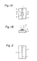
- Figures 1A and 1B illustrate the general principle of the invention.
- a linear aluminum layer 1 is provided on a silicon substrate 4.
- Portion 2 to be cut is coated with an amorphous silicon layer 3 (Fig. lA).
- the reflectivity of aluminum and silicon is 0.92 and 0.41, respectively at wave length of 0.5 ⁇ m.
- the amorphous silicon layer 3 is irradiated by a laser beam 5 (Fig. 1B).
- the laser beam melts the silicon layer 3 and just the portion of the aluminum layer 1 under the silicon layer 3, while leaving the other portions intact. Surface tension then causes the molten aluminum to separate, completing the cut (Fig. 2). During this process, the silicon becomes alloyed with the molten aluminium.
- FIG. 3A An embodiment of the present invention will now be described in detail referring to Figs. 3A to 3D and Figs. 4A and 4B.
- Three linear aluminum layers la.to lc having 1 p m width and spaced 1 ⁇ m from each other are deposited at a thickness of 1 ⁇ m on a silicon dioxide film 4b formed on the silicon substrate 4a.
- a protective phosphorus silicate glass (PSG) film 6 is formed by chemical vapour deposition (Fig. 3A).
- a window 7 is opened in the PSG film 6 by etching it with a mixture of hydrogen fluoride and ammonium fluoride solutions.
- a window 7 is opened in the PSG film 6 by etching it with a mixture of hydrogen fluoride and ammonium fluoride solutions.
- the portion of aluminum layer lb to be cut is exposed (Fig. 3B).
- An amorphous silicon layer 3 is deposited at a thickness of 0.01 to 0.1 ⁇ m (Fig. 3C).
- the layer 3 is then removed, except for the region of aluminum layer lb to be cut, by plasma etching using tetrafluorocarbon (Fig. 3D).
- a continuous wave argon laser beam 5 with an intensity of 9 W having a 5 ⁇ m beam diameter irradiates for 0.1 second the amorphous silicon layer 3, through the window 7, and the PSG film 6 surrounding the window 7 (Figs. 3D, 4A).
- the amorphous silicon layer 3 and the underlying section of the aluminum layer lb melt.
- the aluminum layer lb is then separated at the portion 2 owing to the surface tension of the molten aluminum.
- the other aluminum layers la and lc are not affected by the irradiation of the laser beam (Fig. 4B).
- the amorphous silicon layer 3 is deposited on the aluminum layer lb, whereas the protective PSG film 6 is deposited on the other aluminum layers la and lc (Fig. 3C).
- the protective film is silicon oxynitride (SiON) or polyimide, which can be deposited at a relatively low temperature at which aluminum and amorphous silicon do not alloy with each other, such protective films may be deposited after the amorphous silicon layer is deposited on the aluminum layer.
- polysilicon having higher melting point may be deposited instead of amorphous silicon.
- the present invention enables easy, selective cutting of the electrical conductive layer at the exactly intended portion without damaging other portions, thereby increasing the yield of the products, such as semiconductor devices, and improving the reliability thereof.
Landscapes
- Physics & Mathematics (AREA)
- Engineering & Computer Science (AREA)
- Power Engineering (AREA)
- General Physics & Mathematics (AREA)
- Computer Hardware Design (AREA)
- Microelectronics & Electronic Packaging (AREA)
- Condensed Matter Physics & Semiconductors (AREA)
- High Energy & Nuclear Physics (AREA)
- Manufacturing & Machinery (AREA)
- Optics & Photonics (AREA)
- Electromagnetism (AREA)
- Health & Medical Sciences (AREA)
- Toxicology (AREA)
- Internal Circuitry In Semiconductor Integrated Circuit Devices (AREA)
- Design And Manufacture Of Integrated Circuits (AREA)
- Semiconductor Memories (AREA)
Applications Claiming Priority (2)
| Application Number | Priority Date | Filing Date | Title |
|---|---|---|---|
| JP52100/82 | 1982-03-30 | ||
| JP57052100A JPS58169940A (ja) | 1982-03-30 | 1982-03-30 | 半導体装置の製造方法 |
Publications (3)
| Publication Number | Publication Date |
|---|---|
| EP0090565A2 true EP0090565A2 (fr) | 1983-10-05 |
| EP0090565A3 EP0090565A3 (en) | 1985-06-19 |
| EP0090565B1 EP0090565B1 (fr) | 1989-09-20 |
Family
ID=12905422
Family Applications (1)
| Application Number | Title | Priority Date | Filing Date |
|---|---|---|---|
| EP83301534A Expired EP0090565B1 (fr) | 1982-03-30 | 1983-03-18 | Procédé pour couper sélectivement une couche électroconductrice par irradiation avec un faisceau d'énergie |
Country Status (4)
| Country | Link |
|---|---|
| US (1) | US4476375A (fr) |
| EP (1) | EP0090565B1 (fr) |
| JP (1) | JPS58169940A (fr) |
| DE (1) | DE3380616D1 (fr) |
Cited By (11)
| Publication number | Priority date | Publication date | Assignee | Title |
|---|---|---|---|---|
| EP0189598A1 (fr) * | 1984-12-27 | 1986-08-06 | Kabushiki Kaisha Toshiba | Procédé de fabrication d'un dispositif semi-conducteur |
| EP0208463A1 (fr) * | 1985-06-24 | 1987-01-14 | GOVERNMENT OF THE UNITED STATES OF AMERICA as represented by the US department of energy | Planarisation de couches métalliques pour interconnexions à plusieurs niveaux |
| DE3634167A1 (de) * | 1985-10-09 | 1987-04-16 | Mitsubishi Electric Corp | Redundanzschaltkreis einer halbleitereinrichtung und verfahren zu dessen herstellung |
| DE3741706A1 (de) * | 1987-12-09 | 1989-06-22 | Asea Brown Boveri | Verfahren zur herstellung von spiralfoermigen duennfilm-flachspulen |
| EP0388341A2 (fr) * | 1989-03-14 | 1990-09-19 | International Business Machines Corporation | Procédé et appareil pour causer un circuit ouvert dans une ligne conductrice |
| EP0608764A1 (fr) * | 1993-01-21 | 1994-08-03 | Matsushita Electric Industrial Co., Ltd. | Procédé pour couper des conducteurs et parts de bobines |
| US5374590A (en) * | 1993-04-28 | 1994-12-20 | International Business Machines Corporation | Fabrication and laser deletion of microfuses |
| EP0720229A3 (fr) * | 1994-12-29 | 1998-01-07 | Siemens Aktiengesellschaft | Rangée de fusibles double densité pour programmer d'un circuit intégré ayant un fusible pouvant être fondu par laser |
| GB2338201A (en) * | 1998-06-13 | 1999-12-15 | Exitech Ltd | Laser drilling of holes in materials |
| FR2921752A1 (fr) * | 2007-10-01 | 2009-04-03 | Aplinov Sarl | Procede de chauffage d'une plaque par un flux lumineux. |
| CN107283075A (zh) * | 2017-08-02 | 2017-10-24 | 武汉华星光电半导体显示技术有限公司 | 改善激光切割工艺中倒角区域缺陷的方法 |
Families Citing this family (17)
| Publication number | Priority date | Publication date | Assignee | Title |
|---|---|---|---|---|
| US4604513A (en) * | 1985-05-07 | 1986-08-05 | Lim Basilio Y | Combination of a laser and a controller for trimming a metallized dielectric film capacitor |
| US4745258A (en) * | 1985-08-27 | 1988-05-17 | Mitsubishi Denki Kabushiki Kaisha | Apparatus for laser-cutting metal interconnections in a semiconductor device |
| US5329152A (en) * | 1986-11-26 | 1994-07-12 | Quick Technologies Ltd. | Ablative etch resistant coating for laser personalization of integrated circuits |
| JPS63262621A (ja) * | 1987-04-21 | 1988-10-28 | Alps Electric Co Ltd | 薄膜トランジスタアレイのトリミング方法 |
| DE3834361A1 (de) * | 1988-10-10 | 1990-04-12 | Lsi Logic Products Gmbh | Anschlussrahmen fuer eine vielzahl von anschluessen |
| JPH02112890A (ja) * | 1988-10-20 | 1990-04-25 | Showa Denko Kk | ダイヤモンドの切断方法 |
| US5102830A (en) * | 1990-07-24 | 1992-04-07 | Micron Technology, Inc. | Integrated circuit fabrication process for preventing overprocessing during a laser scan |
| JPH05235170A (ja) * | 1992-02-24 | 1993-09-10 | Nec Corp | 半導体装置 |
| US5963825A (en) * | 1992-08-26 | 1999-10-05 | Hyundai Electronics America | Method of fabrication of semiconductor fuse with polysilicon plate |
| US5747868A (en) * | 1995-06-26 | 1998-05-05 | Alliance Semiconductor Corporation | Laser fusible link structure for semiconductor devices |
| US5759428A (en) * | 1996-03-15 | 1998-06-02 | International Business Machines Corporation | Method of laser cutting a metal line on an MR head |
| DE19924153B4 (de) * | 1999-05-26 | 2006-02-09 | Infineon Technologies Ag | Schaltungsanordnung zur Reparatur eines Halbleiterspeichers |
| US6650519B1 (en) | 1999-08-17 | 2003-11-18 | Seagate Technology Llc | ESD protection by a high-to-low resistance shunt |
| US6432760B1 (en) * | 2000-12-28 | 2002-08-13 | Infineon Technologies Ag | Method and structure to reduce the damage associated with programming electrical fuses |
| JP2003200279A (ja) * | 2001-10-24 | 2003-07-15 | Seiko Epson Corp | 基板の電気配線切断方法及びその装置、並びに電子デバイスの製造方法及びその装置 |
| JP4006994B2 (ja) * | 2001-12-18 | 2007-11-14 | 株式会社リコー | 立体構造体の加工方法、立体形状品の製造方法及び立体構造体 |
| FR2938116B1 (fr) * | 2008-11-04 | 2011-03-11 | Aplinov | Procede et dispositif de chauffage d'une couche d'une plaque par amorcage et flux lumineux. |
Citations (4)
| Publication number | Priority date | Publication date | Assignee | Title |
|---|---|---|---|---|
| DE2705444A1 (de) * | 1977-02-09 | 1978-08-10 | Siemens Ag | Verfahren zur lokal begrenzten erwaermung eines festkoerpers |
| US4238839A (en) * | 1979-04-19 | 1980-12-09 | National Semiconductor Corporation | Laser programmable read only memory |
| EP0025347A2 (fr) * | 1979-09-05 | 1981-03-18 | Fujitsu Limited | Dispositifs semiconducteurs comportant des fusibles |
| JPS56138948A (en) * | 1980-03-31 | 1981-10-29 | Fujitsu Ltd | Manufacture of ic memory |
Family Cites Families (3)
| Publication number | Priority date | Publication date | Assignee | Title |
|---|---|---|---|---|
| US4272775A (en) * | 1978-07-03 | 1981-06-09 | National Semiconductor Corporation | Laser trim protection process and structure |
| JPS5860560A (ja) * | 1981-10-07 | 1983-04-11 | Toshiba Corp | 半導体装置の冗長回路およびそのフユ−ズ部切断方法 |
| JPS5948543B2 (ja) * | 1981-10-13 | 1984-11-27 | 株式会社東芝 | 半導体装置 |
-
1982
- 1982-03-30 JP JP57052100A patent/JPS58169940A/ja active Granted
-
1983
- 1983-03-18 DE DE8383301534T patent/DE3380616D1/de not_active Expired
- 1983-03-18 EP EP83301534A patent/EP0090565B1/fr not_active Expired
- 1983-03-25 US US06/478,721 patent/US4476375A/en not_active Expired - Fee Related
Patent Citations (4)
| Publication number | Priority date | Publication date | Assignee | Title |
|---|---|---|---|---|
| DE2705444A1 (de) * | 1977-02-09 | 1978-08-10 | Siemens Ag | Verfahren zur lokal begrenzten erwaermung eines festkoerpers |
| US4238839A (en) * | 1979-04-19 | 1980-12-09 | National Semiconductor Corporation | Laser programmable read only memory |
| EP0025347A2 (fr) * | 1979-09-05 | 1981-03-18 | Fujitsu Limited | Dispositifs semiconducteurs comportant des fusibles |
| JPS56138948A (en) * | 1980-03-31 | 1981-10-29 | Fujitsu Ltd | Manufacture of ic memory |
Non-Patent Citations (2)
| Title |
|---|
| PATENTS ABSTRACTS OF JAPAN, Vol.6, No.16, (E-92) (894), January 29, 1982. & JP-A-56 138 948 ( FUJITSU K.K. ) (29-10-1981 ) * |
| R.C.A.TECHNICAL NOTES, No.976, September 1974, pages 1.2 - 2.2, PRINCETON,N.J. (US). J.J. FABULA:"Semiconductor fuse". * |
Cited By (17)
| Publication number | Priority date | Publication date | Assignee | Title |
|---|---|---|---|---|
| EP0189598A1 (fr) * | 1984-12-27 | 1986-08-06 | Kabushiki Kaisha Toshiba | Procédé de fabrication d'un dispositif semi-conducteur |
| EP0208463A1 (fr) * | 1985-06-24 | 1987-01-14 | GOVERNMENT OF THE UNITED STATES OF AMERICA as represented by the US department of energy | Planarisation de couches métalliques pour interconnexions à plusieurs niveaux |
| DE3634167A1 (de) * | 1985-10-09 | 1987-04-16 | Mitsubishi Electric Corp | Redundanzschaltkreis einer halbleitereinrichtung und verfahren zu dessen herstellung |
| DE3741706A1 (de) * | 1987-12-09 | 1989-06-22 | Asea Brown Boveri | Verfahren zur herstellung von spiralfoermigen duennfilm-flachspulen |
| EP0388341A2 (fr) * | 1989-03-14 | 1990-09-19 | International Business Machines Corporation | Procédé et appareil pour causer un circuit ouvert dans une ligne conductrice |
| EP0388341A3 (fr) * | 1989-03-14 | 1991-07-17 | International Business Machines Corporation | Procédé et appareil pour causer un circuit ouvert dans une ligne conductrice |
| US5455389A (en) * | 1993-01-21 | 1995-10-03 | Matsushita Electric Industrial Co., Ltd. | Conductor cutting method and coil parts |
| EP0608764A1 (fr) * | 1993-01-21 | 1994-08-03 | Matsushita Electric Industrial Co., Ltd. | Procédé pour couper des conducteurs et parts de bobines |
| US5374590A (en) * | 1993-04-28 | 1994-12-20 | International Business Machines Corporation | Fabrication and laser deletion of microfuses |
| EP0720229A3 (fr) * | 1994-12-29 | 1998-01-07 | Siemens Aktiengesellschaft | Rangée de fusibles double densité pour programmer d'un circuit intégré ayant un fusible pouvant être fondu par laser |
| GB2338201A (en) * | 1998-06-13 | 1999-12-15 | Exitech Ltd | Laser drilling of holes in materials |
| FR2921752A1 (fr) * | 2007-10-01 | 2009-04-03 | Aplinov Sarl | Procede de chauffage d'une plaque par un flux lumineux. |
| WO2009050381A2 (fr) * | 2007-10-01 | 2009-04-23 | Aplinov | Procede de chauffage d'une plaque par un flux lumineux |
| WO2009050381A3 (fr) * | 2007-10-01 | 2009-06-11 | Aplinov | Procede de chauffage d'une plaque par un flux lumineux |
| US8324530B2 (en) | 2007-10-01 | 2012-12-04 | Soitec | Method for heating a wafer by means of a light flux |
| CN107283075A (zh) * | 2017-08-02 | 2017-10-24 | 武汉华星光电半导体显示技术有限公司 | 改善激光切割工艺中倒角区域缺陷的方法 |
| CN107283075B (zh) * | 2017-08-02 | 2019-01-15 | 武汉华星光电半导体显示技术有限公司 | 改善激光切割工艺中倒角区域缺陷的方法 |
Also Published As
| Publication number | Publication date |
|---|---|
| EP0090565B1 (fr) | 1989-09-20 |
| US4476375A (en) | 1984-10-09 |
| DE3380616D1 (en) | 1989-10-26 |
| JPS6412095B2 (fr) | 1989-02-28 |
| EP0090565A3 (en) | 1985-06-19 |
| JPS58169940A (ja) | 1983-10-06 |
Similar Documents
| Publication | Publication Date | Title |
|---|---|---|
| EP0090565B1 (fr) | Procédé pour couper sélectivement une couche électroconductrice par irradiation avec un faisceau d'énergie | |
| EP0162145B1 (fr) | Procédé de faire fondre une connection fusible en utilisant un faisceau laser | |
| US4665295A (en) | Laser make-link programming of semiconductor devices | |
| EP0083211B1 (fr) | Dispositif semi-conducteur comprenant un fusible | |
| US6521971B2 (en) | Metal fuse in copper dual damascene | |
| US4751197A (en) | Make-link programming of semiconductor devices using laser enhanced thermal breakdown of insulator | |
| US4912066A (en) | Make-link programming of semiconductor devices using laser-enhanced thermal breakdown of insulator | |
| US4748491A (en) | Redundant circuit of semiconductor device and method of producing same | |
| US4968643A (en) | Method for fabricating an activatable conducting link for metallic conductive wiring in a semiconductor device | |
| KR920000227B1 (ko) | 반도체장치의 용장회로 | |
| US5936297A (en) | Programmable semiconductor element having an antifuse structure | |
| US5070392A (en) | Integrated circuit having laser-alterable metallization layer | |
| US5288664A (en) | Method of forming wiring of semiconductor device | |
| US5100834A (en) | Method of planarizing metal layer | |
| JP3489088B2 (ja) | 冗長手段を有する半導体装置及びその製造方法 | |
| US5235154A (en) | Laser removal of metal interconnects | |
| EP0999592B1 (fr) | Disposition de fusibles pour un procédé amelioré de fonte de fusibles | |
| JP2793232B2 (ja) | イオンビームによる配線の切断および接続に適した半導体装置 | |
| JPS6193643A (ja) | レ−ザ・ビ−ムでプログラムし得る半導体装置と半導体装置の製法 | |
| JPS6084837A (ja) | 半導体集積回路装置 | |
| JPH09172087A (ja) | 半導体装置 | |
| US20050205965A1 (en) | Semiconductor device having a fuse including an aluminum layer | |
| JPH05166935A (ja) | 半導体装置およびその製造方法 | |
| JPH079942B2 (ja) | 集積回路の基板のドーピングされた領域に導体をレーザによって接続する方法と、該方法を実施して得られる集積回路 | |
| EP0887858A2 (fr) | Couche de protection pour fusible fondu par laser dans des dispositifs semiconducteurs |
Legal Events
| Date | Code | Title | Description |
|---|---|---|---|
| PUAI | Public reference made under article 153(3) epc to a published international application that has entered the european phase |
Free format text: ORIGINAL CODE: 0009012 |
|
| AK | Designated contracting states |
Designated state(s): DE FR GB |
|
| PUAL | Search report despatched |
Free format text: ORIGINAL CODE: 0009013 |
|
| AK | Designated contracting states |
Designated state(s): DE FR GB |
|
| 17P | Request for examination filed |
Effective date: 19851202 |
|
| 17Q | First examination report despatched |
Effective date: 19870327 |
|
| GRAA | (expected) grant |
Free format text: ORIGINAL CODE: 0009210 |
|
| AK | Designated contracting states |
Kind code of ref document: B1 Designated state(s): DE FR GB |
|
| REF | Corresponds to: |
Ref document number: 3380616 Country of ref document: DE Date of ref document: 19891026 |
|
| ET | Fr: translation filed | ||
| PLBE | No opposition filed within time limit |
Free format text: ORIGINAL CODE: 0009261 |
|
| STAA | Information on the status of an ep patent application or granted ep patent |
Free format text: STATUS: NO OPPOSITION FILED WITHIN TIME LIMIT |
|
| 26N | No opposition filed | ||
| PGFP | Annual fee paid to national office [announced via postgrant information from national office to epo] |
Ref country code: FR Payment date: 19911231 Year of fee payment: 10 |
|
| PGFP | Annual fee paid to national office [announced via postgrant information from national office to epo] |
Ref country code: GB Payment date: 19920311 Year of fee payment: 10 |
|
| PGFP | Annual fee paid to national office [announced via postgrant information from national office to epo] |
Ref country code: DE Payment date: 19920522 Year of fee payment: 10 |
|
| PG25 | Lapsed in a contracting state [announced via postgrant information from national office to epo] |
Ref country code: GB Effective date: 19930318 |
|
| GBPC | Gb: european patent ceased through non-payment of renewal fee |
Effective date: 19930318 |
|
| PG25 | Lapsed in a contracting state [announced via postgrant information from national office to epo] |
Ref country code: FR Effective date: 19931130 |
|
| PG25 | Lapsed in a contracting state [announced via postgrant information from national office to epo] |
Ref country code: DE Effective date: 19931201 |
|
| REG | Reference to a national code |
Ref country code: FR Ref legal event code: ST |