EP0162145A1 - Procédé de faire fondre une connection fusible en utilisant un faisceau laser - Google Patents
Procédé de faire fondre une connection fusible en utilisant un faisceau laser Download PDFInfo
- Publication number
- EP0162145A1 EP0162145A1 EP84115741A EP84115741A EP0162145A1 EP 0162145 A1 EP0162145 A1 EP 0162145A1 EP 84115741 A EP84115741 A EP 84115741A EP 84115741 A EP84115741 A EP 84115741A EP 0162145 A1 EP0162145 A1 EP 0162145A1
- Authority
- EP
- European Patent Office
- Prior art keywords
- insulation film
- fuse element
- forming
- semiconductor device
- manufacturing
- Prior art date
- Legal status (The legal status is an assumption and is not a legal conclusion. Google has not performed a legal analysis and makes no representation as to the accuracy of the status listed.)
- Granted
Links
Images

Classifications
-
- H—ELECTRICITY
- H01—ELECTRIC ELEMENTS
- H01L—SEMICONDUCTOR DEVICES NOT COVERED BY CLASS H10
- H01L23/00—Details of semiconductor or other solid state devices
- H01L23/52—Arrangements for conducting electric current within the device in operation from one component to another, i.e. interconnections, e.g. wires, lead frames
- H01L23/522—Arrangements for conducting electric current within the device in operation from one component to another, i.e. interconnections, e.g. wires, lead frames including external interconnections consisting of a multilayer structure of conductive and insulating layers inseparably formed on the semiconductor body
- H01L23/525—Arrangements for conducting electric current within the device in operation from one component to another, i.e. interconnections, e.g. wires, lead frames including external interconnections consisting of a multilayer structure of conductive and insulating layers inseparably formed on the semiconductor body with adaptable interconnections
- H01L23/5256—Arrangements for conducting electric current within the device in operation from one component to another, i.e. interconnections, e.g. wires, lead frames including external interconnections consisting of a multilayer structure of conductive and insulating layers inseparably formed on the semiconductor body with adaptable interconnections comprising fuses, i.e. connections having their state changed from conductive to non-conductive
- H01L23/5258—Arrangements for conducting electric current within the device in operation from one component to another, i.e. interconnections, e.g. wires, lead frames including external interconnections consisting of a multilayer structure of conductive and insulating layers inseparably formed on the semiconductor body with adaptable interconnections comprising fuses, i.e. connections having their state changed from conductive to non-conductive the change of state resulting from the use of an external beam, e.g. laser beam or ion beam
-
- H—ELECTRICITY
- H01—ELECTRIC ELEMENTS
- H01L—SEMICONDUCTOR DEVICES NOT COVERED BY CLASS H10
- H01L21/00—Processes or apparatus adapted for the manufacture or treatment of semiconductor or solid state devices or of parts thereof
- H01L21/02—Manufacture or treatment of semiconductor devices or of parts thereof
- H01L21/04—Manufacture or treatment of semiconductor devices or of parts thereof the devices having at least one potential-jump barrier or surface barrier, e.g. PN junction, depletion layer or carrier concentration layer
- H01L21/18—Manufacture or treatment of semiconductor devices or of parts thereof the devices having at least one potential-jump barrier or surface barrier, e.g. PN junction, depletion layer or carrier concentration layer the devices having semiconductor bodies comprising elements of Group IV of the Periodic System or AIIIBV compounds with or without impurities, e.g. doping materials
- H01L21/26—Bombardment with radiation
- H01L21/263—Bombardment with radiation with high-energy radiation
- H01L21/268—Bombardment with radiation with high-energy radiation using electromagnetic radiation, e.g. laser radiation
-
- H—ELECTRICITY
- H01—ELECTRIC ELEMENTS
- H01L—SEMICONDUCTOR DEVICES NOT COVERED BY CLASS H10
- H01L2924/00—Indexing scheme for arrangements or methods for connecting or disconnecting semiconductor or solid-state bodies as covered by H01L24/00
- H01L2924/0001—Technical content checked by a classifier
- H01L2924/0002—Not covered by any one of groups H01L24/00, H01L24/00 and H01L2224/00
-
- Y—GENERAL TAGGING OF NEW TECHNOLOGICAL DEVELOPMENTS; GENERAL TAGGING OF CROSS-SECTIONAL TECHNOLOGIES SPANNING OVER SEVERAL SECTIONS OF THE IPC; TECHNICAL SUBJECTS COVERED BY FORMER USPC CROSS-REFERENCE ART COLLECTIONS [XRACs] AND DIGESTS
- Y10—TECHNICAL SUBJECTS COVERED BY FORMER USPC
- Y10S—TECHNICAL SUBJECTS COVERED BY FORMER USPC CROSS-REFERENCE ART COLLECTIONS [XRACs] AND DIGESTS
- Y10S148/00—Metal treatment
- Y10S148/055—Fuse
-
- Y—GENERAL TAGGING OF NEW TECHNOLOGICAL DEVELOPMENTS; GENERAL TAGGING OF CROSS-SECTIONAL TECHNOLOGIES SPANNING OVER SEVERAL SECTIONS OF THE IPC; TECHNICAL SUBJECTS COVERED BY FORMER USPC CROSS-REFERENCE ART COLLECTIONS [XRACs] AND DIGESTS
- Y10—TECHNICAL SUBJECTS COVERED BY FORMER USPC
- Y10S—TECHNICAL SUBJECTS COVERED BY FORMER USPC CROSS-REFERENCE ART COLLECTIONS [XRACs] AND DIGESTS
- Y10S148/00—Metal treatment
- Y10S148/093—Laser beam treatment in general
Definitions
- This invention relates to a method of manufacturing a semiconductor device.
- a spare programmable decoder comprising a plurality of programming fuse elements is provided in the chip as the means by which spare circuits can be built into the system.
- the fuse elements of the spare decoder are selectively melted and the decoder is programmed to replace the circuits containing the faulty elements.
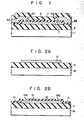
- Fig. 1 is a cross-sectional view of prior art semiconductor, which has a spare decoder comprising programming fuse elements. For the sake of simplicity only one fuse element is shown.
- a prescribed pattern fuse element 3 of polycrystalline silicon is formed on top of a field oxide film 2, which is on a semiconductor substrate 1.
- Fuse element 3 is covered by a thin interlayer insulation film 4.
- Contact holes 5A and 5B are formed in the insulation layer 4 at specified positions leading to the fuse element 3.
- the fuse element 3 is melted by flowing a large current and by radiating a laser beam on the fuse element 3 through passivation film 7 and interlayer insulation film 4. With the decrease in size of the circuit patterns, the laser beam melting method has been used increasingly.
- the strength of the laser beam that is used for melting the fuse element 3 varies with the material and the thickness of the material of the interlayer insulation film 4 and the passivation film 7. If, for example, the material is thick, the energy level must be set higher than when it is thin. There are, however, fluctuations in the thickness of the insulation film, so if the energy level of the laser beam is set for the average thickness, some fuse elements 3 may not be melted. If, in this kind of situation, the energy level of the laser beam is increased to ensure that all the fuse elements will be melted, those regions of the passivation film 7 and interlayer insulation film 4 which are close to the region to be melted of the fuse element 3 will be damaged. Therefore, highly reliable semiconductor devices were not possible with the prior art method of manufacture.
- the object of this invention is to provide a method of manufacturing a semiconductor device by which the melting success rate of the fuse elements is high and the reliability of the products is improved.
- a method of manufacturing a semiconductor device comprising the steps of forming a field insulation film on a semiconductor substrate, forming a fuse element on said field insulation film, forming an interlayer insulation film, which has an opening to said fuse element, on said fuse element, forming wiring layers, which contact said fuse element through said contact holes, on said interlayer insulation film, forming a passivation film, which has an opening passing through said interlayer insulation film and a region corresponding to the region of said fuse element to be melted, over the whole main surface of the resultant structure, melting an exposure region of said interlayer insulation film that is exposed by said opening and said region of said fuse element to be melted using a melting method, and forming a protective layer on the whole surface of the resultant structure after said melting step.
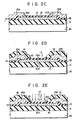
- a field oxide film 11 is formed on a substrate 10 of, for example, silicon, by a thermal oxide method (Fig. 2A).
- a conductive material such as polycrystalline silicon is formed on the field oxide film 11 by CVD (chemical vapour deposition).
- CVD chemical vapour deposition
- a fuse element 12 with a prescribed pattern is formed on the field oxide film 11 using a well-known PEP (photoengraving process) (Fig. 2A).
- an interlayer insulation film 13, of Si0 2 is formed by CVD over the whole main surface of the resultant structure to a thickness of about 3000 A.
- Contact holes 14A, 14B are formed by PEP at prescribed locations in the interlayer insulation film 13 and connect with the fuse element 12 (Fig. 2 B ). These contact holes are for forming semiconductor wiring layers 15A, 15B (to be described later) which contact fuse element 12.
- a conductive layer of, for example, aluminum is formed over the whole main surface of the resultant structure by CVD.
- a conductive layer of, for example, aluminum is formed over the whole main surface of the resultant structure by CVD.
- a conductive layer of, for example, aluminum is formed over the whole main surface of the resultant structure by CVD.
- mutually isolated conducting wiring layers 15A, 15B, which contact fuse element 12 through contact holes 14A, 14B are formed (Fig. 2C).
- a passivation film 16 of, for example, PSG (phosphorous silicon oxide glass) is then formed over the whole main surface of the resultant structure to a thickness of about 10,000 A using CVD.
- This passivation film is then patterned by PEP to form an opening 17 in the region corresponding to the region 12A of fuse element 12 to be melted (Fig. 2D). It is possible to form opening 17 in the same process together with the opening for the bonding pad.
- An exposure region 13A of the interlayer insulation film 13 is irradiated with a YAG laser, for example, through opening 17, as shown by the arrows in Fig. 2E.
- the laser beam is radiated on the region 12A of fuse element 12 to be melted through the region 13A of interlayer insulation film 13 exposed by opening 17.
- the diameter of the laser beam is normally about 5-6 um.
- a resin protective layer 18 is formed over all of the main surface of the resultant structure (Fig. 2G). It is desirable to use a resin having an alpha particle screening function. By screening the alpha particles to the memory cell region (not shown), it is possible to prevent so-called soft errors, thus giving the protective layer 18 two functions. In this case, the protective layer 18 and the layer on the memory cell are formed by the same process so that work can be reduced. If the protective layer 18 is given this kind of dual function, a polyimide resin is used.
- the region of passivation film 16 corresponding to the region 12A of fuse element 12 to be melted is removed beforehand, and with only the interlayer insulation film 13 on the region 12A of the fuse element 12 to be melted, the laser beam is radiated onto the area 12A through the removed region of the passivation film 16 to melt the fuse element 12.
- the laser beam is radiated onto region 12A, not through the thick passivation film 16 of about 10,000 A, but rather only through the relatively thin interlayer insulation film 13. Consequently, uneven melting due to fluctuations in the thickness of the passivation film 16 are eliminated and melting of the fuse element 12 can be performed with a very high success rate.
- the laser beam passes only through a relatively thin interlayer insulation film 13 a high level of energy is not required and, consequently, regions of the passivation film 16 and interlayer insulation film 13 that are close to the region 12A to be melted are not damaged.
- opening 17 is formed in the same process that the bonding pad opening is formed, manufacturing is simplified.
- a method of manufacturing a semiconductor is provided in which the melting success rate is improved without damaging the elements.
Applications Claiming Priority (2)
| Application Number | Priority Date | Filing Date | Title |
|---|---|---|---|
| JP59032830A JPS60176250A (ja) | 1984-02-23 | 1984-02-23 | 半導体装置の製造方法 |
| JP32830/84 | 1984-02-23 |
Publications (2)
| Publication Number | Publication Date |
|---|---|
| EP0162145A1 true EP0162145A1 (fr) | 1985-11-27 |
| EP0162145B1 EP0162145B1 (fr) | 1989-03-08 |
Family
ID=12369740
Family Applications (1)
| Application Number | Title | Priority Date | Filing Date |
|---|---|---|---|
| EP84115741A Expired EP0162145B1 (fr) | 1984-02-23 | 1984-12-18 | Procédé de faire fondre une connection fusible en utilisant un faisceau laser |
Country Status (4)
| Country | Link |
|---|---|
| US (1) | US4602420A (fr) |
| EP (1) | EP0162145B1 (fr) |
| JP (1) | JPS60176250A (fr) |
| DE (1) | DE3477099D1 (fr) |
Cited By (6)
| Publication number | Priority date | Publication date | Assignee | Title |
|---|---|---|---|---|
| EP0307671A2 (fr) * | 1987-09-19 | 1989-03-22 | Texas Instruments Deutschland Gmbh | Procédé pour la fabrication d'un circuit intégré électroprogrammable avec des fusibles de contacts |
| DE3937504A1 (de) * | 1988-11-17 | 1990-05-23 | Mitsubishi Electric Corp | Halbleitereinrichtung mit einem redundanzschaltkreis und verfahren zu deren herstellung |
| EP0374690A1 (fr) * | 1988-12-19 | 1990-06-27 | National Semiconductor Corporation | Structure de connexion fusible programmable permettant la gravure plasma de métaux. |
| GB2237446A (en) * | 1989-10-24 | 1991-05-01 | Seikosha Kk | Fuse for a semi-conductor device |
| US5252844A (en) * | 1988-11-17 | 1993-10-12 | Mitsubishi Denki Kabushiki Kaisha | Semiconductor device having a redundant circuit and method of manufacturing thereof |
| DE19631133A1 (de) * | 1996-01-29 | 1997-07-31 | Mitsubishi Electric Corp | Halbleitervorrichtung mit einer Sicherungsschicht |
Families Citing this family (30)
| Publication number | Priority date | Publication date | Assignee | Title |
|---|---|---|---|---|
| JPS6122650A (ja) * | 1984-07-11 | 1986-01-31 | Hitachi Ltd | 欠陥救済方法および装置 |
| US4924287A (en) * | 1985-01-20 | 1990-05-08 | Avner Pdahtzur | Personalizable CMOS gate array device and technique |
| JPH0821623B2 (ja) * | 1985-09-20 | 1996-03-04 | 株式会社日立製作所 | レ−ザ処理方法 |
| JPH0628290B2 (ja) * | 1985-10-09 | 1994-04-13 | 三菱電機株式会社 | 回路用ヒューズを備えた半導体装置 |
| US4835118A (en) * | 1986-09-08 | 1989-05-30 | Inmos Corporation | Non-destructive energy beam activated conductive links |
| US4826785A (en) * | 1987-01-27 | 1989-05-02 | Inmos Corporation | Metallic fuse with optically absorptive layer |
| IL81849A0 (en) * | 1987-03-10 | 1987-10-20 | Zvi Orbach | Integrated circuits and a method for manufacture thereof |
| IL82113A (en) * | 1987-04-05 | 1992-08-18 | Zvi Orbach | Fabrication of customized integrated circuits |
| US4853758A (en) * | 1987-08-12 | 1989-08-01 | American Telephone And Telegraph Company, At&T Bell Laboratories | Laser-blown links |
| US5182231A (en) * | 1988-04-07 | 1993-01-26 | Hitachi, Ltd. | Method for modifying wiring of semiconductor device |
| US5404029A (en) * | 1990-04-12 | 1995-04-04 | Actel Corporation | Electrically programmable antifuse element |
| US5614756A (en) * | 1990-04-12 | 1997-03-25 | Actel Corporation | Metal-to-metal antifuse with conductive |
| US5780323A (en) * | 1990-04-12 | 1998-07-14 | Actel Corporation | Fabrication method for metal-to-metal antifuses incorporating a tungsten via plug |
| US5241212A (en) * | 1990-05-01 | 1993-08-31 | Mitsubishi Denki Kabushiki Kaisha | Semiconductor device having a redundant circuit portion and a manufacturing method of the same |
| US5236551A (en) * | 1990-05-10 | 1993-08-17 | Microelectronics And Computer Technology Corporation | Rework of polymeric dielectric electrical interconnect by laser photoablation |
| US5285099A (en) * | 1992-12-15 | 1994-02-08 | International Business Machines Corporation | SiCr microfuses |
| US5389814A (en) * | 1993-02-26 | 1995-02-14 | International Business Machines Corporation | Electrically blowable fuse structure for organic insulators |
| US5420455A (en) * | 1994-03-31 | 1995-05-30 | International Business Machines Corp. | Array fuse damage protection devices and fabrication method |
| KR0126101B1 (ko) * | 1994-07-07 | 1997-12-26 | 김주용 | 리페어 마스크 형성방법 |
| TW278229B (en) * | 1994-12-29 | 1996-06-11 | Siemens Ag | Fuse structure for an integrated circuit device and method for manufacturing a fuse structure |
| JPH08222710A (ja) | 1995-02-17 | 1996-08-30 | Mitsubishi Electric Corp | 半導体装置 |
| US5641701A (en) * | 1995-03-30 | 1997-06-24 | Texas Instruments Incorporated | Method for fabricating a semiconductor device with laser programable fuses |
| US6004834A (en) * | 1995-11-29 | 1999-12-21 | Mitsubishi Denki Kabushiki Kaisha | Method of manufacturing semiconductor device having a fuse |
| JPH09153552A (ja) * | 1995-11-29 | 1997-06-10 | Mitsubishi Electric Corp | 半導体装置およびその製造方法 |
| US6025256A (en) * | 1997-01-06 | 2000-02-15 | Electro Scientific Industries, Inc. | Laser based method and system for integrated circuit repair or reconfiguration |
| US5986319A (en) | 1997-03-19 | 1999-11-16 | Clear Logic, Inc. | Laser fuse and antifuse structures formed over the active circuitry of an integrated circuit |
| DE19800566A1 (de) * | 1998-01-09 | 1999-07-15 | Siemens Ag | Verfahren zum Herstellen eines Halbleiterbauelementes und ein derart hergestelltes Halbleiterbauelement |
| US6057180A (en) * | 1998-06-05 | 2000-05-02 | Electro Scientific Industries, Inc. | Method of severing electrically conductive links with ultraviolet laser output |
| US6121074A (en) * | 1998-11-05 | 2000-09-19 | Siemens Aktiengesellschaft | Fuse layout for improved fuse blow process window |
| US7238620B1 (en) | 2004-02-18 | 2007-07-03 | National Semiconductor Corporation | System and method for providing a uniform oxide layer over a laser trimmed fuse with a differential wet etch stop technique |
Citations (3)
| Publication number | Priority date | Publication date | Assignee | Title |
|---|---|---|---|---|
| EP0025347A2 (fr) * | 1979-09-05 | 1981-03-18 | Fujitsu Limited | Dispositifs semiconducteurs comportant des fusibles |
| GB2098300A (en) * | 1981-04-08 | 1982-11-17 | Tracey Stephen | Improvements in and relating to the lining of sewers pipes or the like |
| EP0083211A2 (fr) * | 1981-12-28 | 1983-07-06 | Fujitsu Limited | Dispositif semi-conducteur comprenant un fusible |
Family Cites Families (10)
| Publication number | Priority date | Publication date | Assignee | Title |
|---|---|---|---|---|
| US3330696A (en) * | 1967-07-11 | Method of fabricating thin film capacitors | ||
| US3584183A (en) * | 1968-10-03 | 1971-06-08 | North American Rockwell | Laser encoding of diode arrays |
| US3649806A (en) * | 1970-12-16 | 1972-03-14 | Dieter Konig | Process and apparatus for material excavation by beam energy |
| JPS5641898B2 (fr) * | 1973-08-17 | 1981-10-01 | ||
| US4217570A (en) * | 1978-05-30 | 1980-08-12 | Tektronix, Inc. | Thin-film microcircuits adapted for laser trimming |
| JPS56146268A (en) * | 1980-04-15 | 1981-11-13 | Fujitsu Ltd | Manufacture of semiconductor memory unit |
| JPS5940558B2 (ja) * | 1981-09-17 | 1984-10-01 | 株式会社巴組「鉄」工所 | 板継溶接反転装置 |
| JPS5880852A (ja) * | 1981-11-10 | 1983-05-16 | Toshiba Corp | 半導体装置の製造方法 |
| US4413020A (en) * | 1982-02-01 | 1983-11-01 | Texas Instruments Incorporated | Device fabrication incorporating liquid assisted laser patterning of metallization |
| US4523372A (en) * | 1984-05-07 | 1985-06-18 | Motorola, Inc. | Process for fabricating semiconductor device |
-
1984
- 1984-02-23 JP JP59032830A patent/JPS60176250A/ja active Granted
- 1984-12-13 US US06/681,294 patent/US4602420A/en not_active Expired - Lifetime
- 1984-12-18 EP EP84115741A patent/EP0162145B1/fr not_active Expired
- 1984-12-18 DE DE8484115741T patent/DE3477099D1/de not_active Expired
Patent Citations (3)
| Publication number | Priority date | Publication date | Assignee | Title |
|---|---|---|---|---|
| EP0025347A2 (fr) * | 1979-09-05 | 1981-03-18 | Fujitsu Limited | Dispositifs semiconducteurs comportant des fusibles |
| GB2098300A (en) * | 1981-04-08 | 1982-11-17 | Tracey Stephen | Improvements in and relating to the lining of sewers pipes or the like |
| EP0083211A2 (fr) * | 1981-12-28 | 1983-07-06 | Fujitsu Limited | Dispositif semi-conducteur comprenant un fusible |
Non-Patent Citations (1)
| Title |
|---|
| IBM TECHNICAL DISCLOSURE BULLETIN, vol. 23, no. 10, March 1981, New York, USA; D.E. DAVIS et al. "Passivation process for semiconductor device with fusible link redundancy", pages 4451-4452 * |
Cited By (10)
| Publication number | Priority date | Publication date | Assignee | Title |
|---|---|---|---|---|
| EP0307671A2 (fr) * | 1987-09-19 | 1989-03-22 | Texas Instruments Deutschland Gmbh | Procédé pour la fabrication d'un circuit intégré électroprogrammable avec des fusibles de contacts |
| EP0307671A3 (fr) * | 1987-09-19 | 1990-10-10 | Texas Instruments Deutschland Gmbh | Procédé pour la fabrication d'un circuit intégré électroprogrammable avec des fusibles de contacts |
| DE3937504A1 (de) * | 1988-11-17 | 1990-05-23 | Mitsubishi Electric Corp | Halbleitereinrichtung mit einem redundanzschaltkreis und verfahren zu deren herstellung |
| US5252844A (en) * | 1988-11-17 | 1993-10-12 | Mitsubishi Denki Kabushiki Kaisha | Semiconductor device having a redundant circuit and method of manufacturing thereof |
| EP0374690A1 (fr) * | 1988-12-19 | 1990-06-27 | National Semiconductor Corporation | Structure de connexion fusible programmable permettant la gravure plasma de métaux. |
| GB2237446A (en) * | 1989-10-24 | 1991-05-01 | Seikosha Kk | Fuse for a semi-conductor device |
| GB2237446B (en) * | 1989-10-24 | 1993-07-07 | Seikosha Kk | Semi-conductor device |
| DE19631133A1 (de) * | 1996-01-29 | 1997-07-31 | Mitsubishi Electric Corp | Halbleitervorrichtung mit einer Sicherungsschicht |
| US5872389A (en) * | 1996-01-29 | 1999-02-16 | Mitsubishi Denki Kabushiki Kaisha | Semiconductor device having a fuse layer |
| DE19631133B4 (de) * | 1996-01-29 | 2004-05-06 | Mitsubishi Denki K.K. | Halbleitervorrichtung mit einer Sicherungsschicht |
Also Published As
| Publication number | Publication date |
|---|---|
| DE3477099D1 (en) | 1989-04-13 |
| US4602420A (en) | 1986-07-29 |
| JPS60176250A (ja) | 1985-09-10 |
| EP0162145B1 (fr) | 1989-03-08 |
| JPH0519817B2 (fr) | 1993-03-17 |
Similar Documents
| Publication | Publication Date | Title |
|---|---|---|
| US4602420A (en) | Method of manufacturing a semiconductor device | |
| EP0128675B1 (fr) | Procédé de fabrication d'un circuit intégré à métallisation multicouche avec un fusible et une ouverture pour le fusible | |
| US4622058A (en) | Formation of a multi-layer glass-metallized structure formed on and interconnected to multi-layered-metallized ceramic substrate | |
| US6093630A (en) | Semi-conductor personalization structure and method | |
| EP0075945B1 (fr) | Dispositif semiconducteur empilé et procédé de fabrication | |
| US5023205A (en) | Method of fabricating hybrid circuit structures | |
| EP0075926A2 (fr) | Dispositif semiconducteur à circuit intégré | |
| EP0090565B1 (fr) | Procédé pour couper sélectivement une couche électroconductrice par irradiation avec un faisceau d'énergie | |
| JPH0646648B2 (ja) | レーザ溶断リンクを有する固体回路 | |
| US5844297A (en) | Antifuse device for use on a field programmable interconnect chip | |
| US20090236688A1 (en) | Semiconductor device having fuse pattern and methods of fabricating the same | |
| JPS61145838A (ja) | 半導体素子の接続方法 | |
| KR100675296B1 (ko) | 퓨즈 패턴을 갖는 반도체소자 및 그 제조방법들 | |
| JPH08255553A (ja) | 集積回路装置のためのヒューズ構造部 | |
| KR100741990B1 (ko) | 반도체 장치 및 그 제조 방법 | |
| US5111273A (en) | Fabrication of personalizable integrated circuits | |
| US4855871A (en) | Thin film semiconductor interconnect module | |
| US7067897B2 (en) | Semiconductor device | |
| US4380566A (en) | Radiation protection for integrated circuits utilizing tape automated bonding | |
| US20030062592A1 (en) | Fuse element, semiconductor device and method for manufacturing the same | |
| JP3489088B2 (ja) | 冗長手段を有する半導体装置及びその製造方法 | |
| US5024969A (en) | Hybrid circuit structure fabrication methods using high energy electron beam curing | |
| JPS5948543B2 (ja) | 半導体装置 | |
| US20050205965A1 (en) | Semiconductor device having a fuse including an aluminum layer | |
| JP4236509B2 (ja) | 半導体メモリの製造方法 |
Legal Events
| Date | Code | Title | Description |
|---|---|---|---|
| PUAI | Public reference made under article 153(3) epc to a published international application that has entered the european phase |
Free format text: ORIGINAL CODE: 0009012 |
|
| 17P | Request for examination filed |
Effective date: 19841218 |
|
| AK | Designated contracting states |
Designated state(s): DE FR GB |
|
| 17Q | First examination report despatched |
Effective date: 19870429 |
|
| ITF | It: translation for a ep patent filed |
Owner name: STUDIO JAUMANN |
|
| GRAA | (expected) grant |
Free format text: ORIGINAL CODE: 0009210 |
|
| AK | Designated contracting states |
Kind code of ref document: B1 Designated state(s): DE FR GB |
|
| REF | Corresponds to: |
Ref document number: 3477099 Country of ref document: DE Date of ref document: 19890413 |
|
| ET | Fr: translation filed | ||
| PLBE | No opposition filed within time limit |
Free format text: ORIGINAL CODE: 0009261 |
|
| STAA | Information on the status of an ep patent application or granted ep patent |
Free format text: STATUS: NO OPPOSITION FILED WITHIN TIME LIMIT |
|
| 26N | No opposition filed | ||
| REG | Reference to a national code |
Ref country code: GB Ref legal event code: 746 Effective date: 19980929 |
|
| REG | Reference to a national code |
Ref country code: FR Ref legal event code: D6 |
|
| REG | Reference to a national code |
Ref country code: GB Ref legal event code: IF02 |
|
| PGFP | Annual fee paid to national office [announced via postgrant information from national office to epo] |
Ref country code: FR Payment date: 20031210 Year of fee payment: 20 |
|
| PGFP | Annual fee paid to national office [announced via postgrant information from national office to epo] |
Ref country code: GB Payment date: 20031217 Year of fee payment: 20 |
|
| PGFP | Annual fee paid to national office [announced via postgrant information from national office to epo] |
Ref country code: DE Payment date: 20031229 Year of fee payment: 20 |
|
| PG25 | Lapsed in a contracting state [announced via postgrant information from national office to epo] |
Ref country code: GB Free format text: LAPSE BECAUSE OF EXPIRATION OF PROTECTION Effective date: 20041217 |
|
| REG | Reference to a national code |
Ref country code: GB Ref legal event code: PE20 |