CN1303228A - 发光显示器及其制造方法 - Google Patents
发光显示器及其制造方法 Download PDFInfo
- Publication number
- CN1303228A CN1303228A CN00136448A CN00136448A CN1303228A CN 1303228 A CN1303228 A CN 1303228A CN 00136448 A CN00136448 A CN 00136448A CN 00136448 A CN00136448 A CN 00136448A CN 1303228 A CN1303228 A CN 1303228A
- Authority
- CN
- China
- Prior art keywords
- equipment
- luminescent
- electrode
- luminescent material
- luminescent device
- Prior art date
- Legal status (The legal status is an assumption and is not a legal conclusion. Google has not performed a legal analysis and makes no representation as to the accuracy of the status listed.)
- Pending
Links
- 238000004519 manufacturing process Methods 0.000 title description 3
- 238000004020 luminiscence type Methods 0.000 title 1
- 239000000463 material Substances 0.000 claims abstract description 102
- 238000000034 method Methods 0.000 claims abstract description 21
- 238000007639 printing Methods 0.000 claims abstract description 10
- OAICVXFJPJFONN-UHFFFAOYSA-N Phosphorus Chemical compound [P] OAICVXFJPJFONN-UHFFFAOYSA-N 0.000 claims abstract description 7
- 239000000758 substrate Substances 0.000 claims description 23
- 239000000843 powder Substances 0.000 claims description 16
- 239000000853 adhesive Substances 0.000 claims description 8
- 230000001070 adhesive effect Effects 0.000 claims description 8
- 239000000975 dye Substances 0.000 claims description 6
- 230000015572 biosynthetic process Effects 0.000 claims description 3
- 230000001680 brushing effect Effects 0.000 claims description 2
- 239000006193 liquid solution Substances 0.000 claims 2
- 239000010410 layer Substances 0.000 description 63
- 229920000642 polymer Polymers 0.000 description 51
- 230000005525 hole transport Effects 0.000 description 20
- 239000000243 solution Substances 0.000 description 17
- 125000003983 fluorenyl group Chemical class C1(=CC=CC=2C3=CC=CC=C3CC12)* 0.000 description 16
- -1 polyparaphenylene Polymers 0.000 description 16
- 239000000203 mixture Substances 0.000 description 11
- 125000003118 aryl group Chemical group 0.000 description 9
- 229910052757 nitrogen Inorganic materials 0.000 description 9
- 229910052782 aluminium Inorganic materials 0.000 description 8
- 238000002347 injection Methods 0.000 description 8
- 239000007924 injection Substances 0.000 description 8
- 229920000548 poly(silane) polymer Polymers 0.000 description 8
- XAGFODPZIPBFFR-UHFFFAOYSA-N aluminium Chemical compound [Al] XAGFODPZIPBFFR-UHFFFAOYSA-N 0.000 description 7
- 150000001875 compounds Chemical class 0.000 description 7
- 239000011521 glass Substances 0.000 description 7
- 125000000843 phenylene group Chemical group C1(=C(C=CC=C1)*)* 0.000 description 7
- OKKJLVBELUTLKV-UHFFFAOYSA-N Methanol Chemical compound OC OKKJLVBELUTLKV-UHFFFAOYSA-N 0.000 description 6
- 239000004411 aluminium Substances 0.000 description 6
- 229910052799 carbon Inorganic materials 0.000 description 6
- 229910052751 metal Inorganic materials 0.000 description 6
- 239000002184 metal Substances 0.000 description 6
- QVGXLLKOCUKJST-UHFFFAOYSA-N atomic oxygen Chemical compound [O] QVGXLLKOCUKJST-UHFFFAOYSA-N 0.000 description 5
- 230000005540 biological transmission Effects 0.000 description 5
- 239000002019 doping agent Substances 0.000 description 5
- 238000005516 engineering process Methods 0.000 description 5
- 229910052736 halogen Inorganic materials 0.000 description 5
- MRNHPUHPBOKKQT-UHFFFAOYSA-N indium;tin;hydrate Chemical compound O.[In].[Sn] MRNHPUHPBOKKQT-UHFFFAOYSA-N 0.000 description 5
- 239000012120 mounting media Substances 0.000 description 5
- 229910052760 oxygen Inorganic materials 0.000 description 5
- 239000001301 oxygen Substances 0.000 description 5
- 229920003227 poly(N-vinyl carbazole) Polymers 0.000 description 5
- 229920003229 poly(methyl methacrylate) Polymers 0.000 description 5
- 239000004926 polymethyl methacrylate Substances 0.000 description 5
- IJGRMHOSHXDMSA-UHFFFAOYSA-N Atomic nitrogen Chemical compound N#N IJGRMHOSHXDMSA-UHFFFAOYSA-N 0.000 description 4
- PQMOXTJVIYEOQL-UHFFFAOYSA-N Cumarin Natural products CC(C)=CCC1=C(O)C(C(=O)C(C)CC)=C(O)C2=C1OC(=O)C=C2CCC PQMOXTJVIYEOQL-UHFFFAOYSA-N 0.000 description 4
- FSOGIJPGPZWNGO-UHFFFAOYSA-N Meomammein Natural products CCC(C)C(=O)C1=C(O)C(CC=C(C)C)=C(O)C2=C1OC(=O)C=C2CCC FSOGIJPGPZWNGO-UHFFFAOYSA-N 0.000 description 4
- 125000000217 alkyl group Chemical group 0.000 description 4
- 150000001721 carbon Chemical group 0.000 description 4
- 239000002800 charge carrier Substances 0.000 description 4
- ZYGHJZDHTFUPRJ-UHFFFAOYSA-N coumarin Chemical compound C1=CC=C2OC(=O)C=CC2=C1 ZYGHJZDHTFUPRJ-UHFFFAOYSA-N 0.000 description 4
- 230000006870 function Effects 0.000 description 4
- PQXKHYXIUOZZFA-UHFFFAOYSA-M lithium fluoride Chemical compound [Li+].[F-] PQXKHYXIUOZZFA-UHFFFAOYSA-M 0.000 description 4
- 239000002609 medium Substances 0.000 description 4
- NIHNNTQXNPWCJQ-UHFFFAOYSA-N o-biphenylenemethane Natural products C1=CC=C2CC3=CC=CC=C3C2=C1 NIHNNTQXNPWCJQ-UHFFFAOYSA-N 0.000 description 4
- 238000012545 processing Methods 0.000 description 4
- VYPSYNLAJGMNEJ-UHFFFAOYSA-N silicon dioxide Inorganic materials O=[Si]=O VYPSYNLAJGMNEJ-UHFFFAOYSA-N 0.000 description 4
- 238000004528 spin coating Methods 0.000 description 4
- VEUMBMHMMCOFAG-UHFFFAOYSA-N 2,3-dihydrooxadiazole Chemical compound N1NC=CO1 VEUMBMHMMCOFAG-UHFFFAOYSA-N 0.000 description 3
- 229920002799 BoPET Polymers 0.000 description 3
- 239000005041 Mylar™ Substances 0.000 description 3
- 229920001609 Poly(3,4-ethylenedioxythiophene) Polymers 0.000 description 3
- BQCADISMDOOEFD-UHFFFAOYSA-N Silver Chemical compound [Ag] BQCADISMDOOEFD-UHFFFAOYSA-N 0.000 description 3
- YXFVVABEGXRONW-UHFFFAOYSA-N Toluene Chemical compound CC1=CC=CC=C1 YXFVVABEGXRONW-UHFFFAOYSA-N 0.000 description 3
- 150000001412 amines Chemical class 0.000 description 3
- 239000012298 atmosphere Substances 0.000 description 3
- 239000013522 chelant Substances 0.000 description 3
- 125000004122 cyclic group Chemical group 0.000 description 3
- 239000002270 dispersing agent Substances 0.000 description 3
- PCHJSUWPFVWCPO-UHFFFAOYSA-N gold Chemical compound [Au] PCHJSUWPFVWCPO-UHFFFAOYSA-N 0.000 description 3
- 229910052737 gold Inorganic materials 0.000 description 3
- 239000010931 gold Substances 0.000 description 3
- 150000002367 halogens Chemical class 0.000 description 3
- 239000011777 magnesium Substances 0.000 description 3
- 238000002156 mixing Methods 0.000 description 3
- 230000006798 recombination Effects 0.000 description 3
- 238000005215 recombination Methods 0.000 description 3
- 235000012239 silicon dioxide Nutrition 0.000 description 3
- 229910052709 silver Inorganic materials 0.000 description 3
- 239000004332 silver Substances 0.000 description 3
- 239000002904 solvent Substances 0.000 description 3
- SCYULBFZEHDVBN-UHFFFAOYSA-N 1,1-Dichloroethane Chemical compound CC(Cl)Cl SCYULBFZEHDVBN-UHFFFAOYSA-N 0.000 description 2
- YMMGRPLNZPTZBS-UHFFFAOYSA-N 2,3-dihydrothieno[2,3-b][1,4]dioxine Chemical compound O1CCOC2=C1C=CS2 YMMGRPLNZPTZBS-UHFFFAOYSA-N 0.000 description 2
- OYPRJOBELJOOCE-UHFFFAOYSA-N Calcium Chemical compound [Ca] OYPRJOBELJOOCE-UHFFFAOYSA-N 0.000 description 2
- 241000252203 Clupea harengus Species 0.000 description 2
- LFQSCWFLJHTTHZ-UHFFFAOYSA-N Ethanol Chemical compound CCO LFQSCWFLJHTTHZ-UHFFFAOYSA-N 0.000 description 2
- 239000001856 Ethyl cellulose Substances 0.000 description 2
- ZZSNKZQZMQGXPY-UHFFFAOYSA-N Ethyl cellulose Chemical compound CCOCC1OC(OC)C(OCC)C(OCC)C1OC1C(O)C(O)C(OC)C(CO)O1 ZZSNKZQZMQGXPY-UHFFFAOYSA-N 0.000 description 2
- UFHFLCQGNIYNRP-UHFFFAOYSA-N Hydrogen Chemical compound [H][H] UFHFLCQGNIYNRP-UHFFFAOYSA-N 0.000 description 2
- KFZMGEQAYNKOFK-UHFFFAOYSA-N Isopropanol Chemical compound CC(C)O KFZMGEQAYNKOFK-UHFFFAOYSA-N 0.000 description 2
- FYYHWMGAXLPEAU-UHFFFAOYSA-N Magnesium Chemical compound [Mg] FYYHWMGAXLPEAU-UHFFFAOYSA-N 0.000 description 2
- LRHPLDYGYMQRHN-UHFFFAOYSA-N N-Butanol Chemical class CCCCO LRHPLDYGYMQRHN-UHFFFAOYSA-N 0.000 description 2
- PXHVJJICTQNCMI-UHFFFAOYSA-N Nickel Chemical compound [Ni] PXHVJJICTQNCMI-UHFFFAOYSA-N 0.000 description 2
- 241000233855 Orchidaceae Species 0.000 description 2
- NINIDFKCEFEMDL-UHFFFAOYSA-N Sulfur Chemical compound [S] NINIDFKCEFEMDL-UHFFFAOYSA-N 0.000 description 2
- 239000005864 Sulphur Substances 0.000 description 2
- ATJFFYVFTNAWJD-UHFFFAOYSA-N Tin Chemical compound [Sn] ATJFFYVFTNAWJD-UHFFFAOYSA-N 0.000 description 2
- MCMNRKCIXSYSNV-UHFFFAOYSA-N Zirconium dioxide Chemical compound O=[Zr]=O MCMNRKCIXSYSNV-UHFFFAOYSA-N 0.000 description 2
- 239000002253 acid Substances 0.000 description 2
- 125000003545 alkoxy group Chemical group 0.000 description 2
- MWPLVEDNUUSJAV-UHFFFAOYSA-N anthracene Chemical compound C1=CC=CC2=CC3=CC=CC=C3C=C21 MWPLVEDNUUSJAV-UHFFFAOYSA-N 0.000 description 2
- 230000004888 barrier function Effects 0.000 description 2
- 230000008901 benefit Effects 0.000 description 2
- 229910052791 calcium Inorganic materials 0.000 description 2
- 239000011575 calcium Substances 0.000 description 2
- 239000011248 coating agent Substances 0.000 description 2
- 238000000576 coating method Methods 0.000 description 2
- 238000007796 conventional method Methods 0.000 description 2
- 239000006184 cosolvent Substances 0.000 description 2
- 238000013461 design Methods 0.000 description 2
- 230000006866 deterioration Effects 0.000 description 2
- 238000010586 diagram Methods 0.000 description 2
- 239000003989 dielectric material Substances 0.000 description 2
- 238000003618 dip coating Methods 0.000 description 2
- 230000005684 electric field Effects 0.000 description 2
- 238000005401 electroluminescence Methods 0.000 description 2
- 239000003822 epoxy resin Substances 0.000 description 2
- 150000002148 esters Chemical class 0.000 description 2
- 229920001249 ethyl cellulose Polymers 0.000 description 2
- 235000019325 ethyl cellulose Nutrition 0.000 description 2
- 150000002240 furans Chemical class 0.000 description 2
- 238000010438 heat treatment Methods 0.000 description 2
- 235000019514 herring Nutrition 0.000 description 2
- 125000001183 hydrocarbyl group Chemical group 0.000 description 2
- 229910052739 hydrogen Inorganic materials 0.000 description 2
- 239000001257 hydrogen Substances 0.000 description 2
- 238000005286 illumination Methods 0.000 description 2
- 229910052738 indium Inorganic materials 0.000 description 2
- APFVFJFRJDLVQX-UHFFFAOYSA-N indium atom Chemical compound [In] APFVFJFRJDLVQX-UHFFFAOYSA-N 0.000 description 2
- 239000003446 ligand Substances 0.000 description 2
- 239000007788 liquid Substances 0.000 description 2
- 230000004807 localization Effects 0.000 description 2
- 229910052749 magnesium Inorganic materials 0.000 description 2
- 125000004433 nitrogen atom Chemical group N* 0.000 description 2
- 239000003921 oil Substances 0.000 description 2
- 239000003960 organic solvent Substances 0.000 description 2
- 230000003647 oxidation Effects 0.000 description 2
- 238000007254 oxidation reaction Methods 0.000 description 2
- 239000002245 particle Substances 0.000 description 2
- 238000005424 photoluminescence Methods 0.000 description 2
- IEQIEDJGQAUEQZ-UHFFFAOYSA-N phthalocyanine Chemical compound N1C(N=C2C3=CC=CC=C3C(N=C3C4=CC=CC=C4C(=N4)N3)=N2)=C(C=CC=C2)C2=C1N=C1C2=CC=CC=C2C4=N1 IEQIEDJGQAUEQZ-UHFFFAOYSA-N 0.000 description 2
- 229920000647 polyepoxide Polymers 0.000 description 2
- 238000002360 preparation method Methods 0.000 description 2
- 239000010453 quartz Substances 0.000 description 2
- MCJGNVYPOGVAJF-UHFFFAOYSA-N quinolin-8-ol Chemical compound C1=CN=C2C(O)=CC=CC2=C1 MCJGNVYPOGVAJF-UHFFFAOYSA-N 0.000 description 2
- LIVNPJMFVYWSIS-UHFFFAOYSA-N silicon monoxide Chemical compound [Si-]#[O+] LIVNPJMFVYWSIS-UHFFFAOYSA-N 0.000 description 2
- 238000001228 spectrum Methods 0.000 description 2
- 125000001424 substituent group Chemical group 0.000 description 2
- 239000011135 tin Substances 0.000 description 2
- 229910052718 tin Inorganic materials 0.000 description 2
- 238000012546 transfer Methods 0.000 description 2
- 125000005389 trialkylsiloxy group Chemical group 0.000 description 2
- XLYOFNOQVPJJNP-UHFFFAOYSA-N water Substances O XLYOFNOQVPJJNP-UHFFFAOYSA-N 0.000 description 2
- DXWHZJXKTHGHQF-UHFFFAOYSA-N 2-butyl-6-(butylamino)benzo[de]isoquinoline-1,3-dione Chemical compound O=C1N(CCCC)C(=O)C2=CC=CC3=C2C1=CC=C3NCCCC DXWHZJXKTHGHQF-UHFFFAOYSA-N 0.000 description 1
- DNTVTBIKSZRANH-UHFFFAOYSA-N 4-(4-aminophenyl)-3-(3-methylphenyl)aniline Chemical class CC1=CC=CC(C=2C(=CC=C(N)C=2)C=2C=CC(N)=CC=2)=C1 DNTVTBIKSZRANH-UHFFFAOYSA-N 0.000 description 1
- XLPKAUDSAPXLJO-UHFFFAOYSA-N 4-bromo-2-[[2-[(5-bromo-2-hydroxyphenyl)methylideneamino]phenyl]iminomethyl]phenol Chemical compound OC1=CC=C(Br)C=C1C=NC1=CC=CC=C1N=CC1=CC(Br)=CC=C1O XLPKAUDSAPXLJO-UHFFFAOYSA-N 0.000 description 1
- PLXMOAALOJOTIY-FPTXNFDTSA-N Aesculin Natural products OC[C@@H]1[C@@H](O)[C@H](O)[C@@H](O)[C@H](O)[C@H]1Oc2cc3C=CC(=O)Oc3cc2O PLXMOAALOJOTIY-FPTXNFDTSA-N 0.000 description 1
- 229910001316 Ag alloy Inorganic materials 0.000 description 1
- SZVKJTDZEOTYCX-UHFFFAOYSA-N CN(C1=CC(=C(C=C1)CC1=CC=CC=C1)CN)C Chemical compound CN(C1=CC(=C(C=C1)CC1=CC=CC=C1)CN)C SZVKJTDZEOTYCX-UHFFFAOYSA-N 0.000 description 1
- 101100189588 Canis lupus familiaris PDE6B gene Proteins 0.000 description 1
- OKTJSMMVPCPJKN-UHFFFAOYSA-N Carbon Chemical compound [C] OKTJSMMVPCPJKN-UHFFFAOYSA-N 0.000 description 1
- VGGSQFUCUMXWEO-UHFFFAOYSA-N Ethene Chemical compound C=C VGGSQFUCUMXWEO-UHFFFAOYSA-N 0.000 description 1
- PXGOKWXKJXAPGV-UHFFFAOYSA-N Fluorine Chemical compound FF PXGOKWXKJXAPGV-UHFFFAOYSA-N 0.000 description 1
- 229910000861 Mg alloy Inorganic materials 0.000 description 1
- CBENFWSGALASAD-UHFFFAOYSA-N Ozone Chemical compound [O-][O+]=O CBENFWSGALASAD-UHFFFAOYSA-N 0.000 description 1
- XYFCBTPGUUZFHI-UHFFFAOYSA-N Phosphine Chemical compound P XYFCBTPGUUZFHI-UHFFFAOYSA-N 0.000 description 1
- 239000004698 Polyethylene Substances 0.000 description 1
- 229920000265 Polyparaphenylene Polymers 0.000 description 1
- 239000004743 Polypropylene Substances 0.000 description 1
- 239000004793 Polystyrene Substances 0.000 description 1
- 229910052581 Si3N4 Inorganic materials 0.000 description 1
- BLRPTPMANUNPDV-UHFFFAOYSA-N Silane Chemical compound [SiH4] BLRPTPMANUNPDV-UHFFFAOYSA-N 0.000 description 1
- XUIMIQQOPSSXEZ-UHFFFAOYSA-N Silicon Chemical compound [Si] XUIMIQQOPSSXEZ-UHFFFAOYSA-N 0.000 description 1
- 239000004809 Teflon Substances 0.000 description 1
- 229920006362 Teflon® Polymers 0.000 description 1
- RTAQQCXQSZGOHL-UHFFFAOYSA-N Titanium Chemical compound [Ti] RTAQQCXQSZGOHL-UHFFFAOYSA-N 0.000 description 1
- HCHKCACWOHOZIP-UHFFFAOYSA-N Zinc Chemical compound [Zn] HCHKCACWOHOZIP-UHFFFAOYSA-N 0.000 description 1
- 230000002745 absorbent Effects 0.000 description 1
- 239000002250 absorbent Substances 0.000 description 1
- 230000009102 absorption Effects 0.000 description 1
- 238000010521 absorption reaction Methods 0.000 description 1
- 239000012190 activator Substances 0.000 description 1
- 239000003831 antifriction material Substances 0.000 description 1
- 150000004982 aromatic amines Chemical class 0.000 description 1
- 125000004429 atom Chemical group 0.000 description 1
- 239000011230 binding agent Substances 0.000 description 1
- 235000010290 biphenyl Nutrition 0.000 description 1
- 239000004305 biphenyl Substances 0.000 description 1
- 238000009835 boiling Methods 0.000 description 1
- 239000007767 bonding agent Substances 0.000 description 1
- XZCJVWCMJYNSQO-UHFFFAOYSA-N butyl pbd Chemical compound C1=CC(C(C)(C)C)=CC=C1C1=NN=C(C=2C=CC(=CC=2)C=2C=CC=CC=2)O1 XZCJVWCMJYNSQO-UHFFFAOYSA-N 0.000 description 1
- 239000000969 carrier Substances 0.000 description 1
- 230000003197 catalytic effect Effects 0.000 description 1
- 230000008859 change Effects 0.000 description 1
- 239000003795 chemical substances by application Substances 0.000 description 1
- 125000001309 chloro group Chemical group Cl* 0.000 description 1
- 239000003086 colorant Substances 0.000 description 1
- 150000004696 coordination complex Chemical class 0.000 description 1
- 230000007797 corrosion Effects 0.000 description 1
- 238000005260 corrosion Methods 0.000 description 1
- VBVAVBCYMYWNOU-UHFFFAOYSA-N coumarin 6 Chemical compound C1=CC=C2SC(C3=CC4=CC=C(C=C4OC3=O)N(CC)CC)=NC2=C1 VBVAVBCYMYWNOU-UHFFFAOYSA-N 0.000 description 1
- 125000000113 cyclohexyl group Chemical class [H]C1([H])C([H])([H])C([H])([H])C([H])(*)C([H])([H])C1([H])[H] 0.000 description 1
- 238000000354 decomposition reaction Methods 0.000 description 1
- 238000009792 diffusion process Methods 0.000 description 1
- 238000001035 drying Methods 0.000 description 1
- 238000005538 encapsulation Methods 0.000 description 1
- ZOOODBUHSVUZEM-UHFFFAOYSA-N ethoxymethanedithioic acid Chemical compound CCOC(S)=S ZOOODBUHSVUZEM-UHFFFAOYSA-N 0.000 description 1
- 238000001704 evaporation Methods 0.000 description 1
- 230000008020 evaporation Effects 0.000 description 1
- 230000005281 excited state Effects 0.000 description 1
- 229910052731 fluorine Inorganic materials 0.000 description 1
- 239000011737 fluorine Substances 0.000 description 1
- 239000002223 garnet Substances 0.000 description 1
- YBMRDBCBODYGJE-UHFFFAOYSA-N germanium oxide Inorganic materials O=[Ge]=O YBMRDBCBODYGJE-UHFFFAOYSA-N 0.000 description 1
- 238000000227 grinding Methods 0.000 description 1
- 230000005283 ground state Effects 0.000 description 1
- 125000000623 heterocyclic group Chemical group 0.000 description 1
- XMBWDFGMSWQBCA-UHFFFAOYSA-N hydrogen iodide Chemical compound I XMBWDFGMSWQBCA-UHFFFAOYSA-N 0.000 description 1
- 230000007062 hydrolysis Effects 0.000 description 1
- 238000006460 hydrolysis reaction Methods 0.000 description 1
- 229920001600 hydrophobic polymer Polymers 0.000 description 1
- 229910010272 inorganic material Inorganic materials 0.000 description 1
- 239000011147 inorganic material Substances 0.000 description 1
- 239000011810 insulating material Substances 0.000 description 1
- 238000009413 insulation Methods 0.000 description 1
- 150000002576 ketones Chemical class 0.000 description 1
- 239000011133 lead Substances 0.000 description 1
- 229960004194 lidocaine Drugs 0.000 description 1
- 229910052744 lithium Inorganic materials 0.000 description 1
- WPBNNNQJVZRUHP-UHFFFAOYSA-L manganese(2+);methyl n-[[2-(methoxycarbonylcarbamothioylamino)phenyl]carbamothioyl]carbamate;n-[2-(sulfidocarbothioylamino)ethyl]carbamodithioate Chemical compound [Mn+2].[S-]C(=S)NCCNC([S-])=S.COC(=O)NC(=S)NC1=CC=CC=C1NC(=S)NC(=O)OC WPBNNNQJVZRUHP-UHFFFAOYSA-L 0.000 description 1
- 238000012986 modification Methods 0.000 description 1
- 230000004048 modification Effects 0.000 description 1
- KKFHAJHLJHVUDM-UHFFFAOYSA-N n-vinylcarbazole Chemical compound C1=CC=C2N(C=C)C3=CC=CC=C3C2=C1 KKFHAJHLJHVUDM-UHFFFAOYSA-N 0.000 description 1
- 125000001624 naphthyl group Chemical group 0.000 description 1
- 150000002815 nickel Chemical class 0.000 description 1
- 229910052759 nickel Inorganic materials 0.000 description 1
- VOFUROIFQGPCGE-UHFFFAOYSA-N nile red Chemical compound C1=CC=C2C3=NC4=CC=C(N(CC)CC)C=C4OC3=CC(=O)C2=C1 VOFUROIFQGPCGE-UHFFFAOYSA-N 0.000 description 1
- NICDRCVJGXLKSF-UHFFFAOYSA-N nitric acid;trihydrochloride Chemical compound Cl.Cl.Cl.O[N+]([O-])=O NICDRCVJGXLKSF-UHFFFAOYSA-N 0.000 description 1
- 125000000449 nitro group Chemical group [O-][N+](*)=O 0.000 description 1
- 239000006250 one-dimensional material Substances 0.000 description 1
- 239000011368 organic material Substances 0.000 description 1
- PVADDRMAFCOOPC-UHFFFAOYSA-N oxogermanium Chemical compound [Ge]=O PVADDRMAFCOOPC-UHFFFAOYSA-N 0.000 description 1
- 229960003540 oxyquinoline Drugs 0.000 description 1
- 238000004806 packaging method and process Methods 0.000 description 1
- 238000012856 packing Methods 0.000 description 1
- 125000001997 phenyl group Chemical group [H]C1=C([H])C([H])=C(*)C([H])=C1[H] 0.000 description 1
- ZUOUZKKEUPVFJK-UHFFFAOYSA-N phenylbenzene Natural products C1=CC=CC=C1C1=CC=CC=C1 ZUOUZKKEUPVFJK-UHFFFAOYSA-N 0.000 description 1
- 229910052698 phosphorus Inorganic materials 0.000 description 1
- 239000011574 phosphorus Substances 0.000 description 1
- 229920003023 plastic Polymers 0.000 description 1
- 239000004033 plastic Substances 0.000 description 1
- 230000010287 polarization Effects 0.000 description 1
- 229920003201 poly(di-n-hexylsilylene) polymer Polymers 0.000 description 1
- 229920000573 polyethylene Polymers 0.000 description 1
- 229920006254 polymer film Polymers 0.000 description 1
- 229920000098 polyolefin Polymers 0.000 description 1
- 229920001155 polypropylene Polymers 0.000 description 1
- 229920001296 polysiloxane Polymers 0.000 description 1
- 229920002223 polystyrene Polymers 0.000 description 1
- 230000008569 process Effects 0.000 description 1
- 230000005855 radiation Effects 0.000 description 1
- 238000007761 roller coating Methods 0.000 description 1
- 238000007650 screen-printing Methods 0.000 description 1
- 238000000926 separation method Methods 0.000 description 1
- 229910000077 silane Inorganic materials 0.000 description 1
- 239000010703 silicon Substances 0.000 description 1
- 229910052710 silicon Inorganic materials 0.000 description 1
- 239000000377 silicon dioxide Substances 0.000 description 1
- HQVNEWCFYHHQES-UHFFFAOYSA-N silicon nitride Chemical compound N12[Si]34N5[Si]62N3[Si]51N64 HQVNEWCFYHHQES-UHFFFAOYSA-N 0.000 description 1
- 239000002356 single layer Substances 0.000 description 1
- 239000007787 solid Substances 0.000 description 1
- 239000006104 solid solution Substances 0.000 description 1
- 230000003595 spectral effect Effects 0.000 description 1
- 238000005507 spraying Methods 0.000 description 1
- 230000007480 spreading Effects 0.000 description 1
- 238000003892 spreading Methods 0.000 description 1
- 230000006641 stabilisation Effects 0.000 description 1
- 239000000126 substance Substances 0.000 description 1
- 239000004094 surface-active agent Substances 0.000 description 1
- 239000000725 suspension Substances 0.000 description 1
- 238000003786 synthesis reaction Methods 0.000 description 1
- BFKJFAAPBSQJPD-UHFFFAOYSA-N tetrafluoroethene Chemical compound FC(F)=C(F)F BFKJFAAPBSQJPD-UHFFFAOYSA-N 0.000 description 1
- 238000009210 therapy by ultrasound Methods 0.000 description 1
- 229920001187 thermosetting polymer Polymers 0.000 description 1
- XOLBLPGZBRYERU-UHFFFAOYSA-N tin dioxide Chemical compound O=[Sn]=O XOLBLPGZBRYERU-UHFFFAOYSA-N 0.000 description 1
- 229910001887 tin oxide Inorganic materials 0.000 description 1
- 229910052719 titanium Inorganic materials 0.000 description 1
- 239000010936 titanium Substances 0.000 description 1
- 125000003944 tolyl group Chemical group 0.000 description 1
- 238000001771 vacuum deposition Methods 0.000 description 1
- 238000007740 vapor deposition Methods 0.000 description 1
- 238000005406 washing Methods 0.000 description 1
- 239000012991 xanthate Substances 0.000 description 1
- 229910052725 zinc Inorganic materials 0.000 description 1
- 239000011701 zinc Substances 0.000 description 1
Images


Classifications
-
- H—ELECTRICITY
- H01—ELECTRIC ELEMENTS
- H01L—SEMICONDUCTOR DEVICES NOT COVERED BY CLASS H10
- H01L31/00—Semiconductor devices sensitive to infrared radiation, light, electromagnetic radiation of shorter wavelength or corpuscular radiation and specially adapted either for the conversion of the energy of such radiation into electrical energy or for the control of electrical energy by such radiation; Processes or apparatus specially adapted for the manufacture or treatment thereof or of parts thereof; Details thereof
- H01L31/12—Semiconductor devices sensitive to infrared radiation, light, electromagnetic radiation of shorter wavelength or corpuscular radiation and specially adapted either for the conversion of the energy of such radiation into electrical energy or for the control of electrical energy by such radiation; Processes or apparatus specially adapted for the manufacture or treatment thereof or of parts thereof; Details thereof structurally associated with, e.g. formed in or on a common substrate with, one or more electric light sources, e.g. electroluminescent light sources, and electrically or optically coupled thereto
-
- C—CHEMISTRY; METALLURGY
- C09—DYES; PAINTS; POLISHES; NATURAL RESINS; ADHESIVES; COMPOSITIONS NOT OTHERWISE PROVIDED FOR; APPLICATIONS OF MATERIALS NOT OTHERWISE PROVIDED FOR
- C09D—COATING COMPOSITIONS, e.g. PAINTS, VARNISHES OR LACQUERS; FILLING PASTES; CHEMICAL PAINT OR INK REMOVERS; INKS; CORRECTING FLUIDS; WOODSTAINS; PASTES OR SOLIDS FOR COLOURING OR PRINTING; USE OF MATERIALS THEREFOR
- C09D11/00—Inks
- C09D11/30—Inkjet printing inks
- C09D11/32—Inkjet printing inks characterised by colouring agents
- C09D11/328—Inkjet printing inks characterised by colouring agents characterised by dyes
-
- G—PHYSICS
- G09—EDUCATION; CRYPTOGRAPHY; DISPLAY; ADVERTISING; SEALS
- G09F—DISPLAYING; ADVERTISING; SIGNS; LABELS OR NAME-PLATES; SEALS
- G09F13/00—Illuminated signs; Luminous advertising
- G09F13/20—Illuminated signs; Luminous advertising with luminescent surfaces or parts
- G09F13/22—Illuminated signs; Luminous advertising with luminescent surfaces or parts electroluminescent
-
- H—ELECTRICITY
- H05—ELECTRIC TECHNIQUES NOT OTHERWISE PROVIDED FOR
- H05B—ELECTRIC HEATING; ELECTRIC LIGHT SOURCES NOT OTHERWISE PROVIDED FOR; CIRCUIT ARRANGEMENTS FOR ELECTRIC LIGHT SOURCES, IN GENERAL
- H05B33/00—Electroluminescent light sources
- H05B33/02—Details
-
- H—ELECTRICITY
- H05—ELECTRIC TECHNIQUES NOT OTHERWISE PROVIDED FOR
- H05B—ELECTRIC HEATING; ELECTRIC LIGHT SOURCES NOT OTHERWISE PROVIDED FOR; CIRCUIT ARRANGEMENTS FOR ELECTRIC LIGHT SOURCES, IN GENERAL
- H05B33/00—Electroluminescent light sources
- H05B33/12—Light sources with substantially two-dimensional radiating surfaces
- H05B33/14—Light sources with substantially two-dimensional radiating surfaces characterised by the chemical or physical composition or the arrangement of the electroluminescent material, or by the simultaneous addition of the electroluminescent material in or onto the light source
-
- H—ELECTRICITY
- H05—ELECTRIC TECHNIQUES NOT OTHERWISE PROVIDED FOR
- H05B—ELECTRIC HEATING; ELECTRIC LIGHT SOURCES NOT OTHERWISE PROVIDED FOR; CIRCUIT ARRANGEMENTS FOR ELECTRIC LIGHT SOURCES, IN GENERAL
- H05B33/00—Electroluminescent light sources
- H05B33/12—Light sources with substantially two-dimensional radiating surfaces
- H05B33/22—Light sources with substantially two-dimensional radiating surfaces characterised by the chemical or physical composition or the arrangement of auxiliary dielectric or reflective layers
-
- H—ELECTRICITY
- H10—SEMICONDUCTOR DEVICES; ELECTRIC SOLID-STATE DEVICES NOT OTHERWISE PROVIDED FOR
- H10K—ORGANIC ELECTRIC SOLID-STATE DEVICES
- H10K50/00—Organic light-emitting devices
- H10K50/80—Constructional details
- H10K50/805—Electrodes
-
- H—ELECTRICITY
- H10—SEMICONDUCTOR DEVICES; ELECTRIC SOLID-STATE DEVICES NOT OTHERWISE PROVIDED FOR
- H10K—ORGANIC ELECTRIC SOLID-STATE DEVICES
- H10K59/00—Integrated devices, or assemblies of multiple devices, comprising at least one organic light-emitting element covered by group H10K50/00
- H10K59/10—OLED displays
- H10K59/221—Static displays, e.g. displaying permanent logos
-
- H—ELECTRICITY
- H10—SEMICONDUCTOR DEVICES; ELECTRIC SOLID-STATE DEVICES NOT OTHERWISE PROVIDED FOR
- H10K—ORGANIC ELECTRIC SOLID-STATE DEVICES
- H10K59/00—Integrated devices, or assemblies of multiple devices, comprising at least one organic light-emitting element covered by group H10K50/00
- H10K59/30—Devices specially adapted for multicolour light emission
- H10K59/35—Devices specially adapted for multicolour light emission comprising red-green-blue [RGB] subpixels
-
- H—ELECTRICITY
- H10—SEMICONDUCTOR DEVICES; ELECTRIC SOLID-STATE DEVICES NOT OTHERWISE PROVIDED FOR
- H10K—ORGANIC ELECTRIC SOLID-STATE DEVICES
- H10K59/00—Integrated devices, or assemblies of multiple devices, comprising at least one organic light-emitting element covered by group H10K50/00
- H10K59/30—Devices specially adapted for multicolour light emission
- H10K59/38—Devices specially adapted for multicolour light emission comprising colour filters or colour changing media [CCM]
-
- H—ELECTRICITY
- H10—SEMICONDUCTOR DEVICES; ELECTRIC SOLID-STATE DEVICES NOT OTHERWISE PROVIDED FOR
- H10K—ORGANIC ELECTRIC SOLID-STATE DEVICES
- H10K59/00—Integrated devices, or assemblies of multiple devices, comprising at least one organic light-emitting element covered by group H10K50/00
- H10K59/80—Constructional details
- H10K59/86—Series electrical configurations of multiple OLEDs
-
- H—ELECTRICITY
- H10—SEMICONDUCTOR DEVICES; ELECTRIC SOLID-STATE DEVICES NOT OTHERWISE PROVIDED FOR
- H10K—ORGANIC ELECTRIC SOLID-STATE DEVICES
- H10K71/00—Manufacture or treatment specially adapted for the organic devices covered by this subclass
-
- H—ELECTRICITY
- H01—ELECTRIC ELEMENTS
- H01L—SEMICONDUCTOR DEVICES NOT COVERED BY CLASS H10
- H01L2221/00—Processes or apparatus adapted for the manufacture or treatment of semiconductor or solid state devices or of parts thereof covered by H01L21/00
- H01L2221/67—Apparatus for handling semiconductor or electric solid state devices during manufacture or treatment thereof; Apparatus for handling wafers during manufacture or treatment of semiconductor or electric solid state devices or components; Apparatus not specifically provided for elsewhere
- H01L2221/683—Apparatus for handling semiconductor or electric solid state devices during manufacture or treatment thereof; Apparatus for handling wafers during manufacture or treatment of semiconductor or electric solid state devices or components; Apparatus not specifically provided for elsewhere for supporting or gripping
- H01L2221/68304—Apparatus for handling semiconductor or electric solid state devices during manufacture or treatment thereof; Apparatus for handling wafers during manufacture or treatment of semiconductor or electric solid state devices or components; Apparatus not specifically provided for elsewhere for supporting or gripping using temporarily an auxiliary support
- H01L2221/68359—Apparatus for handling semiconductor or electric solid state devices during manufacture or treatment thereof; Apparatus for handling wafers during manufacture or treatment of semiconductor or electric solid state devices or components; Apparatus not specifically provided for elsewhere for supporting or gripping using temporarily an auxiliary support used as a support during manufacture of interconnect decals or build up layers
-
- H—ELECTRICITY
- H10—SEMICONDUCTOR DEVICES; ELECTRIC SOLID-STATE DEVICES NOT OTHERWISE PROVIDED FOR
- H10K—ORGANIC ELECTRIC SOLID-STATE DEVICES
- H10K50/00—Organic light-emitting devices
- H10K50/80—Constructional details
- H10K50/84—Passivation; Containers; Encapsulations
- H10K50/844—Encapsulations
-
- H—ELECTRICITY
- H10—SEMICONDUCTOR DEVICES; ELECTRIC SOLID-STATE DEVICES NOT OTHERWISE PROVIDED FOR
- H10K—ORGANIC ELECTRIC SOLID-STATE DEVICES
- H10K71/00—Manufacture or treatment specially adapted for the organic devices covered by this subclass
- H10K71/10—Deposition of organic active material
- H10K71/12—Deposition of organic active material using liquid deposition, e.g. spin coating
- H10K71/13—Deposition of organic active material using liquid deposition, e.g. spin coating using printing techniques, e.g. ink-jet printing or screen printing
- H10K71/135—Deposition of organic active material using liquid deposition, e.g. spin coating using printing techniques, e.g. ink-jet printing or screen printing using ink-jet printing
-
- H—ELECTRICITY
- H10—SEMICONDUCTOR DEVICES; ELECTRIC SOLID-STATE DEVICES NOT OTHERWISE PROVIDED FOR
- H10K—ORGANIC ELECTRIC SOLID-STATE DEVICES
- H10K71/00—Manufacture or treatment specially adapted for the organic devices covered by this subclass
- H10K71/841—Applying alternating current [AC] during manufacturing or treatment
-
- H—ELECTRICITY
- H10—SEMICONDUCTOR DEVICES; ELECTRIC SOLID-STATE DEVICES NOT OTHERWISE PROVIDED FOR
- H10K—ORGANIC ELECTRIC SOLID-STATE DEVICES
- H10K85/00—Organic materials used in the body or electrodes of devices covered by this subclass
- H10K85/10—Organic polymers or oligomers
- H10K85/111—Organic polymers or oligomers comprising aromatic, heteroaromatic, or aryl chains, e.g. polyaniline, polyphenylene or polyphenylene vinylene
- H10K85/113—Heteroaromatic compounds comprising sulfur or selene, e.g. polythiophene
- H10K85/1135—Polyethylene dioxythiophene [PEDOT]; Derivatives thereof
-
- H—ELECTRICITY
- H10—SEMICONDUCTOR DEVICES; ELECTRIC SOLID-STATE DEVICES NOT OTHERWISE PROVIDED FOR
- H10K—ORGANIC ELECTRIC SOLID-STATE DEVICES
- H10K85/00—Organic materials used in the body or electrodes of devices covered by this subclass
- H10K85/10—Organic polymers or oligomers
- H10K85/141—Organic polymers or oligomers comprising aliphatic or olefinic chains, e.g. poly N-vinylcarbazol, PVC or PTFE
- H10K85/146—Organic polymers or oligomers comprising aliphatic or olefinic chains, e.g. poly N-vinylcarbazol, PVC or PTFE poly N-vinylcarbazol; Derivatives thereof
-
- H—ELECTRICITY
- H10—SEMICONDUCTOR DEVICES; ELECTRIC SOLID-STATE DEVICES NOT OTHERWISE PROVIDED FOR
- H10K—ORGANIC ELECTRIC SOLID-STATE DEVICES
- H10K85/00—Organic materials used in the body or electrodes of devices covered by this subclass
- H10K85/30—Coordination compounds
- H10K85/321—Metal complexes comprising a group IIIA element, e.g. Tris (8-hydroxyquinoline) gallium [Gaq3]
- H10K85/324—Metal complexes comprising a group IIIA element, e.g. Tris (8-hydroxyquinoline) gallium [Gaq3] comprising aluminium, e.g. Alq3
-
- H—ELECTRICITY
- H10—SEMICONDUCTOR DEVICES; ELECTRIC SOLID-STATE DEVICES NOT OTHERWISE PROVIDED FOR
- H10K—ORGANIC ELECTRIC SOLID-STATE DEVICES
- H10K85/00—Organic materials used in the body or electrodes of devices covered by this subclass
- H10K85/60—Organic compounds having low molecular weight
- H10K85/631—Amine compounds having at least two aryl rest on at least one amine-nitrogen atom, e.g. triphenylamine
-
- H—ELECTRICITY
- H10—SEMICONDUCTOR DEVICES; ELECTRIC SOLID-STATE DEVICES NOT OTHERWISE PROVIDED FOR
- H10K—ORGANIC ELECTRIC SOLID-STATE DEVICES
- H10K85/00—Organic materials used in the body or electrodes of devices covered by this subclass
- H10K85/60—Organic compounds having low molecular weight
- H10K85/649—Aromatic compounds comprising a hetero atom
- H10K85/656—Aromatic compounds comprising a hetero atom comprising two or more different heteroatoms per ring
- H10K85/6565—Oxadiazole compounds
Landscapes
- Engineering & Computer Science (AREA)
- Physics & Mathematics (AREA)
- Chemical & Material Sciences (AREA)
- General Physics & Mathematics (AREA)
- Organic Chemistry (AREA)
- Optics & Photonics (AREA)
- Materials Engineering (AREA)
- Wood Science & Technology (AREA)
- Theoretical Computer Science (AREA)
- Manufacturing & Machinery (AREA)
- Life Sciences & Earth Sciences (AREA)
- Computer Hardware Design (AREA)
- Microelectronics & Electronic Packaging (AREA)
- Power Engineering (AREA)
- Electromagnetism (AREA)
- Condensed Matter Physics & Semiconductors (AREA)
- Electroluminescent Light Sources (AREA)
- Illuminated Signs And Luminous Advertising (AREA)
Abstract
本发明涉及包括第一电极、第二电极、设置在第一和第二电极之间的有机发光层、和从有机发光层接收光并将光转换成不同波长的发光材料的发光显示器,其中第一和第二电极一起确定重叠区域,在该区域中有机发光层被激活发光,发光材料设置在一部分重叠区域中。本发明还涉及一种方法,包括以下步骤:产生图像和在已经形成发光器件之后在包括有机发光层的发光器件上打印图像。该图像可以例如被产生于个人计算机上,并用喷墨打印机打印。该图像被打印在荧光粉上,该荧光粉根据从有机发光层吸收不同波长的光发射一种波长的光。本发明的各个实施例容许终端用户通过向预先形成的、封装的发光器件上施加荧光粉图形而容易地制造定制发光显示器。
Description
本发明一般涉及照明应用,特别涉及包括有机发光材料的显示器件。
长期以来都希望制造一种能够在黑暗中看到的便宜标记。常规措施是利用带有一个或多个滤色器的玻璃或塑料板,其中一个或多个滤色器设置成在放置在背底光上时产生所希望的标记。这样的例子是普通的“EXIT”标记。但是这种技术不容易定制(customizable),因为终端用户不能容易地设计和产生这种标记。大部分终端用户不具有制造滤色板本身所需要的工具或专业知识。因而,终端用户必须获得滤色板制造商的服务以制造定制的标记。大部分终端用户都没有做这种尝试。
已经开发了很多技术以容许在黑暗中可阅读的更易定制的标记。这些技术中大部分在阴极射线管(CRT)显示器上是变化的。这种显示器可以快速地电子地重新设置以显示新的标记。具有这种能力的其它技术包括液晶显示器、薄膜等离子体显示器、和有机电致发光显示器。但是,这些显示器需要很复杂的电子设备并且对于很多简单显示标记应用来说太昂贵了。
因而,长期以来需要一种简单、便宜的能被终端用户很容易地定制的发光标记。
本发明涉及发光显示器,该显示器包括第一电极、第二电极、设置在第一和第二电极之间的有机发光层、和发光材料,该发光材料从有机发光层接收光并将光转换成不同波长,其中第一和第二电极一起确定一个重叠区域,在该重叠区域中有机发光层被激发发光,并且发光材料设置在一部分重叠区域中。
本发明还涉及溶液形式的荧光粉、包括第一电极、第二电极和有机发光层的发光器件和将荧光粉施加到发光器件上的装置。该施加装置可包括例如含有至少一种荧光粉的打印机墨盒。该打印机墨盒可以用于在发光器件上打印发光材料。该施加装置还可包括手动工具,如涂刷、压型器或笔。荧光粉溶液可以以任何所希望的图形和颜色被敷涂、压印或写到发光器件上。
本发明还涉及一种方法,该方法包括以下步骤:产生图像并在形成发光器件之后将图像打印到包括有机发光层的发光器件上。该图像可以例如在个人计算机上形成,并用喷墨打印机打印。该图像可被打印到根据从有机发光层吸收的不同波长的光发射一种波长的光的荧光粉中。
本发明的各种实施例容许被定制的发光显示器被终端用户通过向预制的、封装的发光器件上施加荧光粉图形而容易地制造。该发光器件通常包括在大表面面积上提供照明的有机发光层。荧光粉图形可以用终端用户可得到的很多种方式被施加到发光器件上,如利用计算机打印机或手动工具。计算机产生图像的可利用性容许终端用户用最小设备投资来制造专业质量的发光显示器。
通过下面优选实施例和附图的详细描述使本发明的其它特征和优点更明显,其中:
图1是根据本发明典型实施例的发光显示器的剖面图;
图2-5是根据本发明其它实施例的有机发光层的剖面图;
图6是根据本发明典型实施例的发光显示器的透视图;
图7是根据本发明的典型实施例用于将发光材料施加到发光器件上的装置的示意图;
图8是根据本发明的另一实施例用于将发光材料施加到发光器件上的装置的示意图;
图9是表示根据本发明的典型实施例的发光显示器的发光区的示意图;
图10是根据本发明的另一实施例将发光材料施加到发光器件上的装置的剖面图;
图11是包括多个电极的典型发光显示器的示意图。
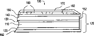
参见图1,其中示出了根据本发明的典型实施例的发光显示器的剖面图。图6表示发光显示器的透视图。发光显示器100包括设置在两个电极即阴极120和阳极130之间的有机发光层110。有机发光层110根据施加在阳极和阴极之间的电压发光。阳极和阴极向有机发光层110中注入电荷载流子即空穴和电子,它们在有机发光层110中复合以形成受激分子或激发子,在该分子或激发子分解时发光。由分子发射的光的颜色取决于分子或激发子的受激态和基态之间的能量差。通常,施加的电压约为3-10伏,但是可以高达30伏或更高,并且外部量子效率(光子输出/电子进入)在0.01%和5%之间或更高。有机发光层110的厚度一般约为50-500nm,电极120、130的厚度一般各为约100-1000nm。
阴极120通常包括具有低功函数值的材料,因而相对小的电压就能使阴极发射电子。阴极120可包括例如钙或如金、铟、锰、锡、铅、铝、银、镁等的一种金属,或者镁/银合金。或者,阴极可以由两层构成以增强电子注入。这样的例子包括LiF的薄内层加上铝或银的较厚外层,或者是钙的薄内层加上铝或银的较厚外层。
阳极130一般包括具有高功函数值的材料。阳极130优选是透明的,因而在有机发光层110中产生的光能够传播到发光显示器100的外部。阳极130可包括例如氧化铟锡(ITO)、氧化锡、镍或金。电极120、130可通过常规汽相淀积技术如蒸发或溅射形成。
各种有机发光层110可与本发明的典型实施例结合使用。根据图1所示的一个实施例,有机发光层110包括单层。有机发光层110可包括例如是发光的共扼聚合物、用电子传输分子和发光材料掺杂的空穴传输聚合物、或用空穴传输分子和发光材料掺杂的惰性聚合物。有机发光层110还可包括能用其它发光分子掺杂的发光小有机分子的非晶膜。
根据图2-5所示的本发明的其它实施例,有机发光层110包括实现空穴注入、空穴传输、电子注入、电子传输和发光功能的两个或多个子层。用于操作器件只需要发光层。但是,附加的子层一般可以提高空穴和电子复合以产生光的效率。因此有机发光层110可包括1-4个子层,例如包括空穴注入子层、空穴传输子层、发光子层和电子注入子层。而且,一个或多个子层可以包括能实现如空穴注入、空穴传输、电子注入、电子传输和发光等两种或更多种功能的材料。
下面介绍有机发光层110包括单层的实施例,如图1所示。
根据第一实施例,有机发光层110包括共扼聚合物。术语共扼聚合物指的是沿着聚合物主链包括不定域π-电子体系的聚合物。不定域π-电子体系给聚合物提供半导电性能并给它支持沿着聚合物链具有高迁移率正和负电荷载流子的能力。聚合物膜具有在电极之间施加电场的足够低浓度的非本征电荷载流子,电荷载流子被注入到聚合物中并从聚合物发射辐射。共扼聚合物例如在R.H.Friend,4Journalof Molecular Electronics37-46(1988)中有论述。
根据施加的电压发光的共扼聚合物的一个例子是PPV(聚对苯撑亚乙烯)。PPV发射在约500-690nm光谱范围内的光并具有良好的耐热性能和抵抗引起破裂的应力的性能。合适的PPV膜通常厚度约为100-1000nm。可通过向衬底上旋涂先导到甲醇中的PPV溶液并在真空炉中加热形成PPV膜。
可以对PPV做各种修改同时保持其发光性能。例如,PPV的亚苯基环可任选地带有一个或多个取代基,各独立地选自烷基、烷氧基、卤素、或硝基。从PPV获得的其它共扼聚合物还可与本发明的典型实施例结合使用。这种PPV衍生物的例子包括:1)用稠环系代替亚苯基环获得的聚合物,例如用蒽或萘环系代替亚苯基环。这些替代环系还可以相对于亚苯基环带有上述类型的一个或多个取代基;2)用杂环系如呋喃环代替亚苯基环获得的聚合物。呋喃环可以与亚苯基环结合带有上述类型的一个或多个取代基;3)通过增加与每个亚苯基或其它环系缔合的1,2-亚乙烯基部分的数量获得的聚合物。上述衍生物具有不同的能隙,这在产生在一个所希望的颜色范围或多个范围内发射的有机发光层110时具有灵活性。关于发光共扼聚合物的附加信息在美国专利5247190中有描述,在这里引用供参考。
合适的共扼聚合物的其它例子包括聚芴,如2,7-取代-9-取代的芴和9-取代芴低聚物和聚合物。芴、低聚物和聚合物用两个烃基部分在9-位置取代,所述烃基部分可任意地含有硫、氮、氧、磷或硅杂原子中的一个或多个;在芴环上形成有9-碳的C5-20环结构或含有硫、氮或氧的一种或多种杂原子的形成有9-碳的C4-20环结构;或者烃基亚基部分。根据一个实施例,芴被芳基部分在2-和7-位置取代,该芳基可进一步用能够交联或链延长的部分或三烷基甲硅烷氧基部分取代。芴聚合物和低聚物可在2-和7’-位置被取代。芴低聚物和聚合物的单体单元在2-和7’-位置彼此键联。通过使在能够交联或链延长的末端2,7’-芳基部分上的任意部分进行链延长或交联,2,7’-芳基-9-取代芴低聚物和聚合物可进一步互相反应,形成较高分子量聚合物。
在极化溶剂中存在二价镍盐的催化量即至少锌粉和三烃基磷化氢的化学计算量的情况下,在2,7-芳基-9-取代芴或9-取代芴低聚物或聚合物被制备的条件下,通过一种或多种2,7-二卤-9-取代芴与一种或多种卤芳族化合物接触,进一步用能交联或链延长的反应基或三烷基甲硅烷氧基部分取代,由此制备2,7-二卤代-9-取代芴或9-取代芴低聚物或聚合物。终止于带有氢或卤素的末端2-和7’-位置的9-取代芴低聚合物和聚合物通过上述工艺在不存在卤芳族化合物的情况下被制备。
芴和芴低聚物或聚合物在固态呈现强光致发光。当这种材料暴露于波长约300到约700nm的光时,这种材料发射的光的波长在约400到约800nm的范围内。更优选的是,这种材料吸收从约350到约400nm的波长的光和发射约400到约650nm范围内的波长的光。本发明的芴和芴低聚物或聚合物在普通有机溶剂中是很容易溶解的。利用如旋涂、喷涂、浸涂和滚涂等常规技术,可将它们加工成薄膜或涂层。在固化时,这种膜呈现出耐普通有机溶剂的性能和高耐热性。关于聚芴的其它信息在美国专利5708130中有介绍,在这里引证供参考。
根据如图1所示的单层器件的第二实施例,有机发光层110包括分子掺杂聚合物。分子掺杂聚合物通常包括在惰性聚合物粘合剂中分子扩散的电荷传输分子的二元固体溶液。该电荷传输分子提高了空穴和电子穿过掺杂聚合物和复合的能力。就可得到的主聚合物粘合剂的掺杂剂材料和机械性能而言惰性聚合物提供很多替换物。
分子掺杂聚合物的一个例子包括用空穴传输分子N,N’-二苯-N,N’-二(3-甲基-苯基)-1,1’-联苯-4,4’-二胺(TPD)和发光材料三(8-羟基喹啉基)-铝(Ⅲ)(Alq)分子掺杂的聚甲基丙烯酸甲酯(PMMA)。TDP具有10-3cm2/volt-sec的高空穴漂移率,而Alq是除了其发光性能外还具有电子传输性能的发光金属络合物。
掺杂浓度通常为约50%,而TDP与Alq的摩尔比例如可以从约0.4到0.1变化。掺杂的PMMA的膜可以通过混合含有合适量的TPD、Alq和PMMA的二氯乙烷溶液并将该溶液浸涂到所希望的衬底上例如氧化铟锡(ITO)电极来制备。掺杂PMMA层的厚度通常为约100nm。当施加电压激活时,产生绿光发射。关于这种掺杂聚合物的其它信息在Junji Kido等人的“Organic Electroluminescent Devices Basedon Molecularly Doped Polymers”,61 Appl.Phys.Lett.761-763(1992)中有介绍,在这里引用供参考。
根据图2所示的本发明另一实施例,有机发光层110包括两个子层。第一子层11提供空穴传输、电子传输和发光性能并与阴极120相邻设置。第二子层12用做空穴注入子层并与阳极130相邻设置。第一子层11包括用电子传输分子和发光材料如染料或聚合物掺杂的空穴传输聚合物。空穴传输聚合物可以包括例如聚(N-乙烯基咔唑)(PVK)。电子传输分子可包括例如2-(4-联苯)-5-(4-叔丁基苯基)-1,3,4-噁二唑(PBD)。发光材料通常包括用做发光中心以改变发射颜色的小分子或聚合物。例如,发光材料可包括有机染料香豆素460(兰)、香豆素6(绿)或尼罗红。上述材料是在市场上可得到,例如从Aldrich Chemical Inc.,Lancaster Synthesis Inc.,TCIAmerica,and Lambda Physik Inc.可得到。可以通过旋涂含有不同量的PVK、电子传输分子、和发光材料的氯仿溶液形成这些混合物的薄膜。例如,合适的混合物包括100重量百分比的PVK、40重量百分比的PBD、和0.2-1.0重量百分比的有机染料。
第二子层12用做空穴注入子层并且可以包括例如从BayerCorporation得到的聚(3,4)亚乙二氧基噻吩/聚苯乙烯磺酸酯(PEDT/PSS),这是通过常规方法如旋涂涂敷的。关于用电子传输分子和发光材料掺杂的空穴传输聚合物的附加信息在Chung-Chih Wu等人的“Efficient Organic Electroluminescent Devices UsingSingle-Layer Doped Polymer Thin Fims with Bipolar CarrierTransport Abilities”,44 IEEE Trans.on Elec.Devices1269-1281(1997)中有介绍,在这里引证供参考。
例1
兰色有机发光器件如下构成。涂有氧化铟锡(ITO)的玻璃(15欧姆-平方)可从Applied Films Corportion购置,并且使用王水蒸气将其部分腐蚀掉。然后这种衬底用洗涤剂机械清洗,浸入在甲醇溶液中,然后浸入在沸腾的异丙醇溶液中,最后放置在臭氧清洁器中5分钟。然后来自Bayer Corportion的聚(3,4)亚乙二氧基噻吩/聚苯乙烯黄酸酯(PEDT/PSS)的近似5纳米(nm)的层被旋涂到ITO上。然后利用二氯乙烷作溶剂将由来自Aldrich公司的聚(9-乙烯基咔唑)(PVK)、来自Aldrich公司的2-(4-联苯)-5-(4-叔丁基苯)-1,3,4-噁二唑(PBD)和来自Exciton公司的7-二乙氨基-4-甲基香豆素(香豆素460)以100∶40∶1重量百分比构成的约100nm的聚合物混合物旋涂到PEDT层上。接着,由约0.8nm的氟化锂层和约100nm的铝构成的阴极通过孔板被蒸发到器件上以确定阴极图形。然后该器件被转移到干燥箱中,并用环氧树脂将玻璃滑板固定到器件的阴极一侧以便封装。得到的器件根据施加电压发射兰光。
根据图3所示的本发明另一实施例,有机发光层110包含包括发光子层的第一子层13和包括空穴传输子层的第二子层14。空穴传输子层14可包括很容易地和可逆地氧化的芳香胺。例如,空穴传输化合物可包括在室温下为固体并且至少一个氮原子被用取代基三取代的胺,其中取代基中至少一个是芳基。空穴传输化合物中的芳基取代基包括芳基和未取代芳基,如苯基和甲苯基。可用的取代基的例子包括1到5个碳原子的烷基、卤素如氯代、氟,和1-5个碳原子的烷氧基,如甲氧基、乙氧基和丙氧基。特殊例子包括1,1-双(4-二-对-甲苯基氨基苯基)环己烷;N,N,N-三(对-甲苯基)胺;1,1-双(4-二-对-甲苯基氨基苯基)-4-苯基环己烷;和2(4-二甲胺基-2-甲基苯基)苯基甲烷。
用于发光子层13的适合的发光材料例子包括4,4’-双(5,7-二-叔戊烷基-2-苯并噁唑基)-茋;2,5-双(5,7-二-叔戊烷基-2-苯并噁唑基)-1,2,4-噻二唑;和8羟基喹啉的金属络合物,这里的金属是Zn、Al、Mg或Li。发光子层13和空穴传输子层14可以利用常规真空淀积技术形成。关于这种器件的附加信息在美国专利4539507中有介绍,在这里引证供参考。
根据图4所示的本发明另一实施例,有机发光层110包括有发光和空穴传输性能的第一子层15,和有电子注入性能的第二子层16。第一子层15包括聚硅烷,第二子层包括噁二唑化合物。这种结构将产生紫外(UV)光。
聚硅烷是用各种烷基和/或芳基侧族取代的线性硅(Si)-主链聚合物。与π共扼聚合物相比,聚硅烷是沿着聚合物主链带有非定域σ共扼电子的准一维材料。由于它们的一维直隙(direct-gap)性质,聚硅烷呈现在紫外区域内的带有高量子效率的强的光致发光性能。合适的聚硅烷的例子包括聚(二-正-丁基硅烷(PDBS))、聚(二-正戊基硅烷)(PDPS)、聚(二-正己基-硅烷)(PDHS)、聚(甲基-苯基硅烷)(PMPS)、和聚[-双(对-丁基苯基)硅烷](PBPS)。例如可以利用旋涂甲苯溶液施加聚硅烷子层15。电子传输子层16可包括例如2,5-双(4-联苯)-1,3,4-噁二唑(BBD)。关于UV-发射的聚硅烷有机发光层的其它信息在Hiroyuki Suzuki等人的“Near-ultraviolet Electroluminescence from Polysilanes”,331 ThinSolid Films 64-70(1998)中有介绍,在这里引证供参考。
根据图5所示的本发明另一实施例,有机发光层110包括空穴注入子层17、空穴传输子层18、发光子层19和电子注入子层20。空穴注入子层17和空穴传输子层18有效地将空穴提供给复合区域。电子注入子层20有效地将电子提供给复合区域。
空穴注入子层17可包括卟啉化合物,如不含金属的酞菁或含有金属的酞菁。空穴传输子层18可包括空穴传输芳族叔胺,后者是含有至少一个只键合到碳原子上的三价氮原子的化合物,其中至少一个碳原子是芳族环成分。发光子层19可包括例如在兰光波长内发射的混合配位体铝螯合物,如双(R-8-喹啉醇基)-(酚-ato)铝(Ⅲ)螯合物,其中R是被选择以阻止两个以上的8-喹啉并-lato配位体附着于铝原子上的8-喹啉醇基环核的环取代基。电子注入子层20可包括金属oxinoid电荷接受化合物,如铝的三-螯合物。关于这种四层材料和器件的附加信息在美国专利5294870中有介绍,这里引证供参考。
有机发光层110的上述例子可用于设计发射一种或多种所希望的颜色的发光器件。例如,发光器件135可发射紫外、兰、绿和红光的一种或多种。可以通过向相同电极的不同区域施加具有不同成分的两个或多个有机发光层110形成不同色区。术语“发光器件”一般指有机发光层110、阴极120和阳极130的结合体。如图1所示,发光器件135还可包括衬底140。衬底140提供基底,在形成过程中可以在该衬底上淀积阳极130、有机发光层110和阴极120。衬底可以包括例如玻璃或透明聚合物,如MYLAR。发光器件135和发光材料160一起形成发光显示器100。
发光器件135可被封装在封装层150内。封装层150优选提供水和氧阻挡性能以减少或防止有机发光层110和电极120、130的氧化和水解劣化。封装层150可包括无机材料,如可以用环氧树脂附着到阴极120上的玻璃或石英。在附着于阴极120上的玻璃封装层情况下,衬底140通常还可以是玻璃或石英,并且用做封装层,因而图1中所示的与衬底140相邻的部分封装层150可以省略。密封部件152可沿着器件的周边设置,将与阴极120相邻的封装层150密封到与阳极130相邻的封装层150上。密封部件152可包括金属,如锡、铟、钛、金或其混合物。
根据又一实施例,封装层150或其部分可包括聚合物,如用介质材料如一氧化硅、二氧化硅、氮化硅、氧化锗或氧化锆涂敷的MYLAR。如果需要的话,可向介质材料上施加一层疏水聚合物,如聚硅氧烷、TEFLON、或分支聚烯烃,例如聚乙烯或聚丙烯。根据该实施例,封装层150还可用做衬底140,以便可省略分离的衬底140。其它封装方法和材料在美国专利5874804和5952778中有介绍,这里引证供参考。
如图1所示,发光材料160施加于发光器件135表面上。发光材料160吸收一部分电磁波谱中的能量并发射另一部分电磁波谱中的能量,与本领域公知的一样。通常,发光材料160包括无机荧光粉。很多无机荧光粉具有一般对氧或潮气不敏感的优点。因而,它们可以被施加于封装发光器件135的外部而不会由于时间长而显著劣化。但是,也可使用其它类型的发光材料如有机荧光材料。
合适的红光发射无机荧光粉的例子是SrB4O7:Sm2+,其中Sm2+遵循颜色表示活化剂。该荧光粉吸收比600nm短的大部分可见光波长并发射作为具有大于650nm波长的深红色线的光。SrB4O7:Sm2+可以通过混合SrCO3、5%过量的H3BO3、Sm2O3,并将混合物在900℃下在还原气氛下例如在5%氢中加热5小时制备。其它合适的红光发射荧光粉包括由Sm2+激活的SrB6O10、BaMgF4和LiBaF3、BaFCl。
合适的黄光发射无机荧光粉的例子是Y3Al5O12:Ce3+。这种荧光粉吸收低于500nm的大部分波长并具有在约570-580nm的最大发射。可以通过将Y2O3、Al2O3、CeO2与用做助溶剂的3摩尔百分比AlF3混合来制备Y3Al5O12:Ce3+。然后将该混合物在轻还原气氛中在1500℃下加热6-8小时。
合适的绿光发射无机荧光粉的例子是SrGa2S4:Eu2+。该荧光粉吸收低于500nm的波长并具有在535纳米的最大发射。可通过例如混合Ga2O3、SrCO3和Eu2O3并在900℃在H2S气流下加热4小时,然后在相同条件下在1000℃研磨和再处理来制备SrGa2S4:Eu2+。
合适的兰光发射无机荧光粉的例子是BaMg2Al16O27:Eu2+。BaMg2Al16O27:Eu2+吸收430nm以下的大部分波长并具有在450nm的最大发射。BaMg2Al16O27:Eu2+可通过在1400℃在还原气氛中焙烧BaCO3、MgO、Al2O3和Eu2O3的混合物来制备。
能用做发光材料160的有机荧光材料的例子是7-二乙氨基-4-甲基香豆素(来自Exciton公司的香豆素460),它吸收低于420nm的波长并发射兰光;3-(2’-苯并噻唑基)-7-二乙氨基香豆素(来自Exciton公司的香豆素540),它吸收500nm以下波长并发射绿光;4-氰亚甲基-2-甲基-6-(对-二甲氨基苯乙烯基)-4H-吡喃(来自Exciton公司的DCM),它吸收550nm以下波长并发射红光;来自Exciton公司的Fluorol 7GA,它吸收低于500nm的波长并发射黄光;3,3’-二乙基氧杂羧基-anine碘化物(来自Exciton公司的DOCI),它吸收500nm以下波长并发射绿光;Nile红-(Adrich公司),它吸收600nm以下波长并发射红光。
发光材料160可吸收由有机发光层110发射的所有光或只吸收部分光。例如,发光材料160可吸收由有机发光层110发射的所有兰光并发射红光。或者,例如发光材料160只吸收由有机发光层110发射的一部分光并发射黄光。在这种情况下,未被吸收的兰光和由荧光粉发射的黄光结合以产生另一种颜色的光,如白光。
发光材料160可以用各种方法施加于发光器件135上。例如,根据一个实施例,发光材料160与载体介质结合并用普通打印机如喷墨打印机施加于发光器件135上。在发光材料160包括无机荧光粉的情况下,无机荧光粉通常在载体介质中是不溶的,而是以小粒子形式分散或悬浮并且相对于凝聚稳定化和被分散剂固定。合适的悬浮液的例子包括在液体介质中的约15体积百分比的荧光粉粉末(例如铯激活的钇铝石榴石)。该荧光粉粉末颗粒尺寸通常为约10微米。构成主要液体介质的溶剂包括例如1-丁醇。还可以添加的是0.5重量百分比的作为粘合剂的乙基纤维素和5.0重量百分比的作为分散剂的鲱鱼油。该材料被超声波处理15分钟以均匀地分散粉末和破坏软附聚物。
在发光材料160包括有机染料情况下,有机染料通常可以溶解在载体介质中。该载体介质可以包括例如水,如果需要的话,还可以包括水溶性助溶剂,如乙醇、酮或酯。还可以添加表面活性剂以调节溶液的表面张力,如本领域公知的那样。
图8表示根据本发明的典型实施例用于向发光器件135施加发光材料160的装置200。该装置200包括计算机210、打印机220、监视器230和键盘240。在其它部件当中计算机210包括存储器212、中心处理单元214、随机存取存储器216、和调制解调器218。存储器212储存如数字图像等信息。中心处理单元214如本领域公知那样处理指令。调制解调器218提供与计算机网络如互联网的接口,并且可从互联网接收数字图像。打印机220从计算机210接收数据如图像数据,并根据数据打印图像。打印机220可包括根据命令向衬底如发光器件135传送至少一种荧光粉溶液的墨盒222。打印机墨盒222可包括例如荧光粉溶液的三个容器,即红、绿和兰,它们被打印到衬底上以产生彩色图像。
发光器件135可以设计成具有标准纸张尺寸,如8.5×11英寸,A4尺寸等,并具有合适的挠性和厚度,以便装配到标准打印机如喷墨打印机上。因而,多色计算机图像可以用商业上可得到的软件设计并被打印到发光器件135上。此外,可用打印机向发光器件135施加多层发光材料160。例如,发绿光的荧光粉可以被施加于整个发光器件135上,其它一种或多种荧光粉可以按图形形式施加于一部分发绿光的荧光粉上。
在发光器件135不装配到标准打印机中或者不够柔软情况下,图像被打印到中间衬底上。例如,荧光粉图形被打印到具有透明粘合剂底层的8.5×11英寸透明材料片上。然后其上具有荧光粉图形的打印中间衬底可以借助粘合剂底层粘接到发光器件135上。通过这种方式可以形成各种形状的发光器件,后者被终端用户定制。图10表示具有粘合剂底层164和发光材料160的这种衬底162的剖面。当然,除了被设计成在常规纸张尺寸上打印的常规喷墨打印机以外,图像还可以用任何大面积喷射打印机打印,
根据本发明的其它实施例,发光材料160利用手动工具用合适的载体介质施加于发光器件135上。发光材料160可以与载体介质混合并被彩色封装。用于无机荧光粉的合适载体介质可以包括例如带有作为粘接剂的0.5重量百分比乙基纤维素和作为分散剂的5.0重量百分比鲱鱼油的1-丁醇,如上所述。图7表示含有三种不同荧光粉即红、绿和兰的溶液的三个容器245。图7还展示了手动工具250。该手动工具250可以是例如涂刷、压型器或笔。然后荧光粉溶液以任意所希望的图形和颜色被涂刷、压制或写到发光器件135上。
根据本发明的另一实施例,使用丝网印刷向发光器件或中间衬底上施加荧光粉溶液。含有所希望图形的一个或多个丝网可利用常规方法制备,荧光粉溶液通过丝网被施加于发光器件135上,将丝网图形传递到发光器件上。
在荧光粉溶液已经被施加于发光器件135上之后, 荧光粉溶液被干燥,留下发光层160,如图1所示。发光层160在发光器件135上形成图形。通常,发光层160不覆盖发光器件135的整个发光区域。发光区域一般由两个电极120、130的重叠区域确定。如图9所示,重叠区域300被定义为电极120、130重叠的区域。电极通常具有基本上相同形状的周边。一般情况下,重叠区域300在某种意义上讲是连续的,不是分立的、分离区域,但也不是单个区域。在重叠区域300中产生电场,从而使有机发光层110发光。如图9所示,发光材料160例如荧光粉通常占据重叠区域300的一部分而不是全部。
发光材料160可以采取数字、字母、装饰设计、或其它任何希望的形式。它可包括多种颜色。图6中所示的电源180可包括根据预置时间表例如一秒闪烁一次给发光显示器100施加电压的控制器。
根据图11所示的本发明另一实施例,发光显示器100包括至少两组独立可操作的电极。在图11中,第一组电极控制发光显示器100的第一部分102,第二组电极控制第二部分104。这些电极经过引线103、105与电源180相连。电源180可包括控制器以独立地激活第一和第二组电极。例如,如图11所示,“NO”部分102可以独立于“VACACNY”部分而被接通或截止。如果需要的话,电极可以根据预置时间表独立地操作。在多组电极的情况下,每组电极可借助电绝缘材料107与其它组电极电绝缘。
再参见图1,对于抗磨性来说,可以在发光材料160上施加抗磨层170。该抗磨层170可包括透明的、抗磨材料如MYLAR或其它透明聚合物。抗磨层170可包括用于将抗磨层170粘接到发光器件135和发光材料160上的粘合剂底层。如果发光材料160包括无机荧光粉,就不需要抗磨层170来提供氧或潮气阻挡性能,因为很多无机荧光粉是相对稳定的。
对于本领域技术人员来说考虑到这里公开的实施例就可使本发明的其它实施例显而易见。因此说明书和实施例只是示意性的,本发明的范围和实质应当由所附权利要求书来确定。
Claims (35)
1.一种设备,包括:
第一电极;
第二电极;
设置在第一和第二电极之间的有机发光层,其中第一和第二电极一起确定重叠区域,在该重叠区域中有机发光层被激活发光;和
发光材料,从有机发光层接收光并将光转换成不同波长,其中发光材料设置在一部分重叠区域中。
2.权利要求1的设备,其中第一和第二电极的周边具有基本上相同的形状。
3.权利要求1的设备,其中发光材料占据一部分重叠区域以在重叠区域中产生图形。
4.权利要求1的设备,其中发光材料包括至少一种无机荧光粉。
5.权利要求1的设备,其中发光材料包括至少一种有机染料。
6.权利要求1的设备,其中发光材料包括SrB4O7:Sm2+、Y3Al5O12:Ce3+、SrGa2S4:Eu2+、和BaMg2Al16O27:Eu2+中的至少一种。
7.权利要求1的设备,其中有机发光层发射紫外光。
8.权利要求1的设备,其中该设备具有矩形周边,该周边具有A4纸或8.5×11英寸纸的尺寸。
9.权利要求1的设备,还包括发射第二种颜色光的第二发光材料。
10.权利要求1的设备,其中发光材料包括第一层发光材料和设置在第一层发光材料上的第二层发光材料。
11.权利要求1的设备,还包括独立于第一和第二电极操作的第三电极和第四电极。
12.权利要求1的设备,还包括设置在发光材料和第一电极之间的封装层。
13.权利要求12的设备,还包括其上施加发光材料的透明衬底,其中透明衬底包括粘合剂底层。
14.权利要求13的设备,其中透明衬底用粘合剂底层粘接到封装层上。
15.一种包括含有至少一种溶液形式的荧光粉的打印机墨盒的设备。
16.权利要求15的设备,还包括发光器件,该发光器件包括第一电极、第二电极、和设置在第一和第二电极之间的有机发光层。
17.权利要求15的设备,其中打印机墨盒是喷墨打印机墨盒。
18.权利要求15的设备,其中至少一种荧光粉包括发绿光荧光粉和发红光荧光粉。
19.权利要求15的设备,其中至少一种荧光粉包括SrB4O7:Sm2+、Y3Al5O12:Ce3+、SrGa2S4:Eu2+、和BaMg2Al16O27:Eu2+中的至少一种。
20.一种设备,包括:
溶液形式的荧光粉;
包括第一电极、第二电极、和有机发光层的发光器件;和
向发光器件上施加荧光粉的装置。
21.权利要求20的设备,其中施加装置包括打印机墨盒。
22.权利要求20的设备,其中施加装置包括涂刷。
23.权利要求20的设备,其中施加装置包括笔。
24.一种方法,包括以下步骤:
通过形成第一电极、形成第二电极、和在第一和第二电极之间形成有机发光层,形成发光器件;和
在已经形成发光器件之后,以发光材料能施加到发光器件上的形式提供发光材料。
25.权利要求24的方法,其中发光材料包括荧光粉,并且提供步骤包括形成荧光粉的液体溶液的步骤。
26.权利要求25的方法,其中提供步骤包括在打印机墨盒中封装液体溶液的步骤。
27.权利要求24的方法,其中形成发光器件的步骤还包括形成独立于第一和第二电极操作的第三电极和第四电极的步骤。
28.一种方法,包括以下步骤:
产生图像;和
在已经形成发光器件之后,在包括有机发光层的发光器件上打印图像。
29.权利要求28的方法,其中图像在计算机上产生。
30.权利要求28的方法,其中打印步骤包括打印第一层和在第一层上打印第二层。
31.权利要求28的方法,其中打印步骤包括在发光器件上打印荧光粉溶液。
32.权利要求31的方法,还包括在打印图像上施加抗磨层的步骤。
33.权利要求28的方法,其中打印步骤包括在发光器件上打印多色荧光粉图形。
34.权利要求28的方法,其中打印步骤包括用喷墨打印机在发光器件上打印图像。
35.一种方法,包括以下步骤:
产生图像;
在衬底上打印图像;和
将打印衬底固定到包括有机发光层的发光器件上。
Applications Claiming Priority (2)
| Application Number | Priority Date | Filing Date | Title |
|---|---|---|---|
| US09/469,702 | 1999-12-22 | ||
| US09/469,702 US6566808B1 (en) | 1999-12-22 | 1999-12-22 | Luminescent display and method of making |
Publications (1)
| Publication Number | Publication Date |
|---|---|
| CN1303228A true CN1303228A (zh) | 2001-07-11 |
Family
ID=23864769
Family Applications (1)
| Application Number | Title | Priority Date | Filing Date |
|---|---|---|---|
| CN00136448A Pending CN1303228A (zh) | 1999-12-22 | 2000-12-22 | 发光显示器及其制造方法 |
Country Status (7)
| Country | Link |
|---|---|
| US (3) | US6566808B1 (zh) |
| EP (1) | EP1111966A3 (zh) |
| JP (1) | JP2001297879A (zh) |
| KR (1) | KR20010062574A (zh) |
| CN (1) | CN1303228A (zh) |
| CA (1) | CA2327870A1 (zh) |
| TW (1) | TW513896B (zh) |
Cited By (5)
| Publication number | Priority date | Publication date | Assignee | Title |
|---|---|---|---|---|
| CN102569659A (zh) * | 2010-12-27 | 2012-07-11 | 苏州晶能科技有限公司 | 有机无机led面光源模块及其制造方法 |
| WO2018210142A1 (zh) * | 2017-05-19 | 2018-11-22 | 中国科学院化学研究所 | 一种打印激光光源的打印头模块、系统及方法 |
| US10453900B2 (en) | 2017-05-03 | 2019-10-22 | Boe Technology Group Co., Ltd. | Display panel, driving method thereof, and display device |
| CN110456560A (zh) * | 2019-07-29 | 2019-11-15 | 武汉华星光电技术有限公司 | 一种显示面板及其显示装置 |
| CN113764598A (zh) * | 2020-06-03 | 2021-12-07 | 咸阳彩虹光电科技有限公司 | 一种薄膜封装结构、oled显示面板及显示器 |
Families Citing this family (125)
| Publication number | Priority date | Publication date | Assignee | Title |
|---|---|---|---|---|
| US7768210B2 (en) * | 1999-12-22 | 2010-08-03 | General Electric Company | Hybrid electroluminescent devices |
| US7576496B2 (en) * | 1999-12-22 | 2009-08-18 | General Electric Company | AC powered OLED device |
| US6566808B1 (en) * | 1999-12-22 | 2003-05-20 | General Electric Company | Luminescent display and method of making |
| US20020190661A1 (en) * | 2000-01-27 | 2002-12-19 | General Electric Company | AC powered oled device |
| DE10005296A1 (de) * | 2000-02-07 | 2001-08-16 | Infineon Technologies Ag | Vorrichtung für die Emission elektromagnetischer Strahlung und Verfahren zu deren Herstellung |
| JP2002090737A (ja) * | 2000-09-18 | 2002-03-27 | Hitachi Ltd | 液晶表示装置 |
| JP4273694B2 (ja) * | 2001-06-07 | 2009-06-03 | セイコーエプソン株式会社 | Elディスプレイ、el照明装置、およびその駆動方法、ならびに液晶装置および電子機器 |
| FI110675B (fi) * | 2001-07-06 | 2003-03-14 | Valtion Teknillinen | Menetelmä orgaanisen valoa emittoivan diodin muokkaamiseksi |
| US20030068470A1 (en) * | 2001-08-17 | 2003-04-10 | Eastman Kodak Company | Combination of imaging member and functional base for new utility |
| US6970512B2 (en) * | 2001-08-28 | 2005-11-29 | Sbc Technology Resources, Inc. | Method and system to improve the transport of compressed video data |
| TWI264121B (en) * | 2001-11-30 | 2006-10-11 | Semiconductor Energy Lab | A display device, a method of manufacturing a semiconductor device, and a method of manufacturing a display device |
| US6660184B2 (en) * | 2001-12-13 | 2003-12-09 | Osram Sylvania Inc. | Phosphor paste compositions |
| US6953735B2 (en) | 2001-12-28 | 2005-10-11 | Semiconductor Energy Laboratory Co., Ltd. | Method for fabricating a semiconductor device by transferring a layer to a support with curvature |
| WO2003069957A1 (fr) * | 2002-02-12 | 2003-08-21 | Idemitsu Kosan Co., Ltd. | Ecran electroluminescent et son procede de fabrication |
| JP3838964B2 (ja) * | 2002-03-13 | 2006-10-25 | 株式会社リコー | 機能性素子基板の製造装置 |
| TW200403956A (en) * | 2002-07-01 | 2004-03-01 | Seiko Epson Corp | Composition, film formation method and device, photoelectric device and its manufacturing method, organic EL device and its manufacturing method, device, manufacturing method and electronic machine |
| US7049757B2 (en) | 2002-08-05 | 2006-05-23 | General Electric Company | Series connected OLED structure and fabrication method |
| US7034470B2 (en) * | 2002-08-07 | 2006-04-25 | Eastman Kodak Company | Serially connecting OLED devices for area illumination |
| EP2149907A3 (en) * | 2002-08-29 | 2014-05-07 | Seoul Semiconductor Co., Ltd. | Light-emitting device having light-emitting diodes |
| EP1563523A4 (en) | 2002-09-03 | 2006-05-24 | Bloomberg Lp | DECK RINGLESS ELECTRONIC DISPLAY |
| US6919678B2 (en) * | 2002-09-03 | 2005-07-19 | Bloomberg Lp | Bezel-less electric display |
| US7224116B2 (en) | 2002-09-11 | 2007-05-29 | Osram Opto Semiconductors Gmbh | Encapsulation of active electronic devices |
| US20040048033A1 (en) * | 2002-09-11 | 2004-03-11 | Osram Opto Semiconductors (Malaysia) Sdn. Bhd. | Oled devices with improved encapsulation |
| US7193364B2 (en) * | 2002-09-12 | 2007-03-20 | Osram Opto Semiconductors (Malaysia) Sdn. Bhd | Encapsulation for organic devices |
| US20040135160A1 (en) * | 2003-01-10 | 2004-07-15 | Eastman Kodak Company | OLED device |
| US7279832B2 (en) * | 2003-04-01 | 2007-10-09 | Innovalight, Inc. | Phosphor materials and illumination devices made therefrom |
| US20040252488A1 (en) * | 2003-04-01 | 2004-12-16 | Innovalight | Light-emitting ceiling tile |
| KR101142648B1 (ko) * | 2003-05-21 | 2012-05-10 | 다우 글로벌 테크놀로지스 엘엘씨 | 점도 개질제 및 발광성 화합물의 블렌드 |
| US20040238846A1 (en) * | 2003-05-30 | 2004-12-02 | Georg Wittmann | Organic electronic device |
| US7145125B2 (en) | 2003-06-23 | 2006-12-05 | Advanced Optical Technologies, Llc | Integrating chamber cone light using LED sources |
| US7521667B2 (en) | 2003-06-23 | 2009-04-21 | Advanced Optical Technologies, Llc | Intelligent solid state lighting |
| JP2007502534A (ja) * | 2003-08-12 | 2007-02-08 | コーニンクレッカ フィリップス エレクトロニクス エヌ ヴィ | 有機ダイオードの交流駆動用回路配置 |
| DE10339941A1 (de) * | 2003-08-29 | 2005-03-24 | BSH Bosch und Siemens Hausgeräte GmbH | Kältegerät mit OLED-Display |
| US7012585B2 (en) * | 2004-02-06 | 2006-03-14 | Eastman Kodak Company | OLED apparatus having improved fault tolerance |
| EP1759145A1 (en) * | 2004-05-28 | 2007-03-07 | Tir Systems Ltd. | Luminance enhancement apparatus and method |
| US7733441B2 (en) | 2004-06-03 | 2010-06-08 | Semiconductor Energy Labortory Co., Ltd. | Organic electroluminescent lighting system provided with an insulating layer containing fluorescent material |
| US20060012289A1 (en) * | 2004-07-19 | 2006-01-19 | General Electric Company | Hybrid electroluminescent devices |
| GB2416621A (en) * | 2004-07-27 | 2006-02-01 | Cambridge Display Tech Ltd | Laminated interconnects for opto-electronic device modules |
| US7750352B2 (en) * | 2004-08-10 | 2010-07-06 | Pinion Technologies, Inc. | Light strips for lighting and backlighting applications |
| US20060038485A1 (en) * | 2004-08-18 | 2006-02-23 | Harvatek Corporation | Laminated light-emitting diode display device and manufacturing method thereof |
| US7348738B2 (en) * | 2004-09-02 | 2008-03-25 | General Electric Company | OLED area illumination source |
| TWI240438B (en) * | 2004-09-07 | 2005-09-21 | Opto Tech Corp | High power LED array |
| CA2580402A1 (en) * | 2004-09-15 | 2006-03-23 | Holyoke Consulting Llc | Device for the signalling and lighting during an emergency condition |
| US8013519B2 (en) * | 2004-12-06 | 2011-09-06 | Koninklijke Philips Electronics N.V. | Organic electroluminescent light source |
| US7259391B2 (en) * | 2004-12-22 | 2007-08-21 | General Electric Company | Vertical interconnect for organic electronic devices |
| US7307278B2 (en) * | 2004-12-22 | 2007-12-11 | General Electric Company | Organic electronic devices having two dimensional series interconnections |
| US20060145599A1 (en) * | 2005-01-04 | 2006-07-06 | Reza Stegamat | OLEDs with phosphors |
| US20060214577A1 (en) * | 2005-03-26 | 2006-09-28 | Lorraine Byrne | Depositing of powdered luminescent material onto substrate of electroluminescent lamp |
| US7518148B2 (en) * | 2005-03-29 | 2009-04-14 | General Electric Company | Full fault tolerant architecture for organic electronic devices |
| US7645177B2 (en) * | 2005-05-07 | 2010-01-12 | Hewlett-Packard Development Company, L.P. | Electroluminescent panel with inkjet-printed electrode regions |
| EP1905069B1 (en) * | 2005-07-14 | 2011-03-16 | Philips Intellectual Property & Standards GmbH | Electroluminescent light source |
| US7781023B2 (en) * | 2005-10-11 | 2010-08-24 | Hewlett-Packard Development Company, L.P. | Method of producing an electroluminescent display |
| WO2007047779A1 (en) * | 2005-10-14 | 2007-04-26 | University Of Florida Research Foundation, Inc. | Method and apparatus for light emission utilizing an oled with a microcavity |
| KR100571882B1 (ko) * | 2005-10-27 | 2006-04-17 | 알티전자 주식회사 | 황색 형광체 및 이를 포함하는 백색 발광 장치 |
| US7843134B2 (en) * | 2005-10-31 | 2010-11-30 | Idemitsu Kosan Co., Ltd. | Organic EL emission devices connected in series |
| EP1860923A1 (en) * | 2006-05-22 | 2007-11-28 | TETENAL AG & Co. KG. | Electroluminescent element |
| US7926300B2 (en) | 2005-11-18 | 2011-04-19 | Cree, Inc. | Adaptive adjustment of light output of solid state lighting panels |
| US8278846B2 (en) | 2005-11-18 | 2012-10-02 | Cree, Inc. | Systems and methods for calibrating solid state lighting panels |
| US8514210B2 (en) | 2005-11-18 | 2013-08-20 | Cree, Inc. | Systems and methods for calibrating solid state lighting panels using combined light output measurements |
| CN103925521A (zh) * | 2005-12-21 | 2014-07-16 | 科锐公司 | 照明装置 |
| US20070144045A1 (en) * | 2005-12-23 | 2007-06-28 | Lexmark International, Inc. | Electroluminescent display system |
| KR101157265B1 (ko) * | 2005-12-30 | 2012-06-15 | 엘지디스플레이 주식회사 | 유기전계 발광표시장치 |
| KR101084166B1 (ko) * | 2006-01-13 | 2011-11-17 | 삼성모바일디스플레이주식회사 | 픽셀 구조 및 이를 구비한 유기 전계 발광소자 |
| US7629742B2 (en) * | 2006-03-17 | 2009-12-08 | Lexmark International, Inc. | Electroluminescent displays, media, and members, and methods associated therewith |
| US7648257B2 (en) | 2006-04-21 | 2010-01-19 | Cree, Inc. | Light emitting diode packages |
| US7777166B2 (en) | 2006-04-21 | 2010-08-17 | Cree, Inc. | Solid state luminaires for general illumination including closed loop feedback control |
| KR100805038B1 (ko) * | 2006-05-04 | 2008-02-20 | 주식회사 엘지화학 | 유기발광소자 및 그의 제조방법 |
| WO2007130536A2 (en) | 2006-05-05 | 2007-11-15 | Cree Led Lighting Solutions, Inc. | Lighting device |
| US8008676B2 (en) | 2006-05-26 | 2011-08-30 | Cree, Inc. | Solid state light emitting device and method of making same |
| US8596819B2 (en) | 2006-05-31 | 2013-12-03 | Cree, Inc. | Lighting device and method of lighting |
| US7969097B2 (en) | 2006-05-31 | 2011-06-28 | Cree, Inc. | Lighting device with color control, and method of lighting |
| US20080007936A1 (en) * | 2006-07-05 | 2008-01-10 | Jie Liu | Organic illumination source and method for controlled illumination |
| US7766508B2 (en) | 2006-09-12 | 2010-08-03 | Cree, Inc. | LED lighting fixture |
| US7665862B2 (en) | 2006-09-12 | 2010-02-23 | Cree, Inc. | LED lighting fixture |
| WO2008064717A1 (de) * | 2006-11-30 | 2008-06-05 | Osram Opto Semiconductors Gmbh | Strukturanordnung und verfahren zur ausfallsicherung einer led- oder oled-kette |
| EP1927973B1 (de) | 2006-11-30 | 2017-05-03 | OSRAM OLED GmbH | Strukturanordnung und Verfahren zur Ausfallsicherung einer LED- oder OLED-Kette |
| US7498603B2 (en) * | 2006-12-06 | 2009-03-03 | General Electric Company | Color tunable illumination source and method for controlled illumination |
| US8258682B2 (en) | 2007-02-12 | 2012-09-04 | Cree, Inc. | High thermal conductivity packaging for solid state light emitting apparatus and associated assembling methods |
| JP4356899B2 (ja) * | 2007-03-15 | 2009-11-04 | 財団法人山形県産業技術振興機構 | 有機el発光装置およびその製造方法 |
| US7824070B2 (en) | 2007-03-22 | 2010-11-02 | Cree, Inc. | LED lighting fixture |
| US7625502B2 (en) * | 2007-03-26 | 2009-12-01 | General Electric Company | Nano-scale metal halide scintillation materials and methods for making same |
| US7608829B2 (en) * | 2007-03-26 | 2009-10-27 | General Electric Company | Polymeric composite scintillators and method for making same |
| US7708968B2 (en) | 2007-03-26 | 2010-05-04 | General Electric Company | Nano-scale metal oxide, oxyhalide and oxysulfide scintillation materials and methods for making same |
| US7781779B2 (en) * | 2007-05-08 | 2010-08-24 | Luminus Devices, Inc. | Light emitting devices including wavelength converting material |
| US8042971B2 (en) | 2007-06-27 | 2011-10-25 | Cree, Inc. | Light emitting device (LED) lighting systems for emitting light in multiple directions and related methods |
| WO2009012287A1 (en) | 2007-07-17 | 2009-01-22 | Cree Led Lighting Solutions, Inc. | Optical elements with internal optical features and methods of fabricating same |
| DE102007052181A1 (de) * | 2007-09-20 | 2009-04-02 | Osram Opto Semiconductors Gmbh | Optoelektronisches Bauelement und Verfahren zur Herstellung eines optoelektronischen Bauelements |
| US8866410B2 (en) | 2007-11-28 | 2014-10-21 | Cree, Inc. | Solid state lighting devices and methods of manufacturing the same |
| DE102008046857A1 (de) | 2007-12-17 | 2009-06-18 | Osram Opto Semiconductors Gmbh | OLED für Betrieb mit Wechselspannung und Herstellungsverfahren |
| US7804245B2 (en) * | 2008-01-24 | 2010-09-28 | Global Oled Technology Llc | Electroluminescent device having improved brightness uniformity |
| US20090252933A1 (en) * | 2008-04-04 | 2009-10-08 | 3M Innovative Properties Company | Method for digitally printing electroluminescent lamps |
| US8240875B2 (en) | 2008-06-25 | 2012-08-14 | Cree, Inc. | Solid state linear array modules for general illumination |
| TW201000602A (en) * | 2008-06-30 | 2010-01-01 | Paragon Technologies Co Ltd | Organic membrane for transmitting optical spectrum and LED chip package module |
| WO2010022101A2 (en) * | 2008-08-19 | 2010-02-25 | Plextronics, Inc. | Organic light emitting diode lighting devices |
| TWI446822B (zh) * | 2008-10-28 | 2014-07-21 | Nat Univ Tsing Hua | 有機發光二極體裝置及其製造方法 |
| US8022631B2 (en) * | 2008-11-03 | 2011-09-20 | General Electric Company | Color control of light sources employing phosphors |
| FR2941033A1 (fr) * | 2009-01-15 | 2010-07-16 | Peugeot Citroen Automobiles Sa | Bloc optique a amplification de photons par luminescence |
| TWI466266B (zh) * | 2009-02-24 | 2014-12-21 | Epistar Corp | 陣列式發光元件及其裝置 |
| US20100294526A1 (en) * | 2009-05-21 | 2010-11-25 | General Electric Company | Hermetic electrical package |
| US8450926B2 (en) | 2009-05-21 | 2013-05-28 | General Electric Company | OLED lighting devices including electrodes with magnetic material |
| US8427845B2 (en) * | 2009-05-21 | 2013-04-23 | General Electric Company | Electrical connectors for optoelectronic device packaging |
| DE102009050542A1 (de) | 2009-10-23 | 2011-04-28 | Merck Patent Gmbh | Sm-aktivierte Aluminat- und Borat-Leuchtstoffe |
| US8188463B2 (en) * | 2009-11-19 | 2012-05-29 | General Electric Company | Organic light emitting diode with magnetic structure for improved current adaptability |
| US20110163337A1 (en) * | 2010-01-06 | 2011-07-07 | General Electric Company | Architecture for organic electronic devices |
| JP2012009420A (ja) | 2010-05-21 | 2012-01-12 | Semiconductor Energy Lab Co Ltd | 発光装置及び照明装置 |
| WO2012014759A1 (en) | 2010-07-26 | 2012-02-02 | Semiconductor Energy Laboratory Co., Ltd. | Light-emitting device, lighting device, and manufacturing method of light-emitting device |
| JP5827885B2 (ja) | 2010-12-24 | 2015-12-02 | 株式会社半導体エネルギー研究所 | 発光装置及び照明装置 |
| JP6000127B2 (ja) * | 2011-01-07 | 2016-09-28 | 株式会社カネカ | 有機el装置 |
| JP5964070B2 (ja) * | 2011-02-10 | 2016-08-03 | 株式会社半導体エネルギー研究所 | 照明装置 |
| JP5820295B2 (ja) | 2011-02-21 | 2015-11-24 | 株式会社半導体エネルギー研究所 | 照明装置 |
| US8373181B2 (en) | 2011-06-29 | 2013-02-12 | General Electric Company | Method and device for a cathode structure for flexible organic light emitting diode (OLED) device |
| US8552420B2 (en) | 2011-08-09 | 2013-10-08 | Universal Display Corporation | OLED light panel with controlled brightness variation |
| RU2614515C2 (ru) * | 2011-12-05 | 2017-03-28 | Филипс Лайтинг Холдинг Б.В. | Осветительная система |
| KR101926358B1 (ko) * | 2012-02-17 | 2018-12-07 | 삼성전자주식회사 | 반도체 발광장치 및 조명장치 |
| US20130248914A1 (en) | 2012-03-20 | 2013-09-26 | General Electric Company | Packaged optoelectronic device and process for manufacturing |
| US20130278158A1 (en) * | 2012-03-26 | 2013-10-24 | Cheorwon Plasma Research Institute | Oled lighting module |
| DE102012109142B4 (de) * | 2012-09-27 | 2019-04-25 | Osram Oled Gmbh | Verfahren zum Herstellen eines passiven elektronischen Bauelements und Verfahren zum Herstellen einer optoelektronischen Baugruppe |
| JP2014102958A (ja) | 2012-11-19 | 2014-06-05 | Toshiba Corp | 表示装置及び表示システム |
| WO2014129519A1 (en) | 2013-02-20 | 2014-08-28 | Semiconductor Energy Laboratory Co., Ltd. | Peeling method, semiconductor device, and peeling apparatus |
| KR20150033195A (ko) * | 2013-09-23 | 2015-04-01 | 삼성디스플레이 주식회사 | 유기 발광 표시 장치 및 그 제조 방법 |
| CN105793957B (zh) | 2013-12-12 | 2019-05-03 | 株式会社半导体能源研究所 | 剥离方法及剥离装置 |
| US20160335933A1 (en) * | 2014-01-08 | 2016-11-17 | Julie Claire Company Limited | A submersible display |
| CA3105969A1 (en) * | 2018-07-13 | 2020-01-16 | Roger MCKENZIE | Hybrid led / photoluminescent signs |
| US11739919B2 (en) | 2019-07-10 | 2023-08-29 | Inspace Media Ltd. | Panel, system, kit of parts and methods |
| CN112586990B (zh) * | 2020-12-01 | 2022-02-01 | 杭州九阳小家电有限公司 | 一种烹饪器具 |
Family Cites Families (41)
| Publication number | Priority date | Publication date | Assignee | Title |
|---|---|---|---|---|
| US3558886A (en) * | 1969-04-23 | 1971-01-26 | David Carver | Method of discovering imperfections in bonded laminated structures |
| US3763468A (en) * | 1971-10-01 | 1973-10-02 | Energy Conversion Devices Inc | Light emitting display array with non-volatile memory |
| US4186020A (en) * | 1974-11-04 | 1980-01-29 | A. B. Dick Company | Fluorescent ink for automatic identification |
| JPS538053A (en) * | 1976-07-09 | 1978-01-25 | Fujitsu Ltd | Gas discharging panel |
| US4539507A (en) | 1983-03-25 | 1985-09-03 | Eastman Kodak Company | Organic electroluminescent devices having improved power conversion efficiencies |
| IT209813Z2 (it) * | 1987-01-08 | 1988-11-04 | Incas Int Carbon Solvent Spa | Nastro adesivo fluorescente atto all'impiego com evidenziatore. |
| US4769292A (en) | 1987-03-02 | 1988-09-06 | Eastman Kodak Company | Electroluminescent device with modified thin film luminescent zone |
| GB8909011D0 (en) | 1989-04-20 | 1989-06-07 | Friend Richard H | Electroluminescent devices |
| US5294870A (en) | 1991-12-30 | 1994-03-15 | Eastman Kodak Company | Organic electroluminescent multicolor image display device |
| JPH06337647A (ja) * | 1993-05-28 | 1994-12-06 | Nec Kansai Ltd | 電界発光灯表示板及びその製造方法 |
| US5681380A (en) * | 1995-06-05 | 1997-10-28 | Kimberly-Clark Worldwide, Inc. | Ink for ink jet printers |
| JPH0864009A (ja) * | 1994-08-17 | 1996-03-08 | Mitsuru Kono | 平面蛍光発色薄型装飾装置 |
| JP3187695B2 (ja) * | 1995-02-06 | 2001-07-11 | 出光興産株式会社 | 多色発光装置およびその製造方法 |
| JPH08330070A (ja) * | 1995-05-29 | 1996-12-13 | Pioneer Electron Corp | 発光素子の駆動法 |
| US5708130A (en) | 1995-07-28 | 1998-01-13 | The Dow Chemical Company | 2,7-aryl-9-substituted fluorenes and 9-substituted fluorene oligomers and polymers |
| JP2947154B2 (ja) * | 1996-01-31 | 1999-09-13 | 日本精機株式会社 | 電界発光素子 |
| WO1997038347A1 (en) * | 1996-04-10 | 1997-10-16 | Cambridge Display Technology Limited | Efficient backlighting for lcds |
| US5772741A (en) | 1996-05-20 | 1998-06-30 | E. I. Du Pont De Nemours And Company | Aqueous ink jet ink compositions |
| AUPO062996A0 (en) * | 1996-06-24 | 1996-07-18 | Zone Properties Pty Ltd | Ink composition |
| US5661645A (en) * | 1996-06-27 | 1997-08-26 | Hochstein; Peter A. | Power supply for light emitting diode array |
| JPH1039791A (ja) * | 1996-07-22 | 1998-02-13 | Mitsubishi Electric Corp | 有機エレクトロルミネッセンス表示装置 |
| TW383508B (en) * | 1996-07-29 | 2000-03-01 | Nichia Kagaku Kogyo Kk | Light emitting device and display |
| US5705285A (en) * | 1996-09-03 | 1998-01-06 | Motorola, Inc. | Multicolored organic electroluminescent display |
| US5874803A (en) | 1997-09-09 | 1999-02-23 | The Trustees Of Princeton University | Light emitting device with stack of OLEDS and phosphor downconverter |
| US6013982A (en) * | 1996-12-23 | 2000-01-11 | The Trustees Of Princeton University | Multicolor display devices |
| US5965242A (en) * | 1997-02-19 | 1999-10-12 | Eastman Kodak Company | Glow-in-the-dark medium and method of making |
| US5874804A (en) | 1997-03-03 | 1999-02-23 | Motorola, Inc. | Organic electroluminescent device hermetic encapsulation package and method of fabrication |
| US5952778A (en) | 1997-03-18 | 1999-09-14 | International Business Machines Corporation | Encapsulated organic light emitting device |
| US6337492B1 (en) * | 1997-07-11 | 2002-01-08 | Emagin Corporation | Serially-connected organic light emitting diode stack having conductors sandwiching each light emitting layer |
| JPH1167451A (ja) * | 1997-08-20 | 1999-03-09 | Idemitsu Kosan Co Ltd | 有機el発光装置及び多色発光装置 |
| JPH1187055A (ja) * | 1997-09-11 | 1999-03-30 | Shibusawa Enterp Kk | シート状発光表示装置および発光表示装置 |
| US6370019B1 (en) * | 1998-02-17 | 2002-04-09 | Sarnoff Corporation | Sealing of large area display structures |
| JP3884564B2 (ja) * | 1998-05-20 | 2007-02-21 | 出光興産株式会社 | 有機el発光素子およびそれを用いた発光装置 |
| ITTO980580A1 (it) | 1998-07-02 | 2000-01-02 | C R F Societa Consotile Per Az | Dispositivo emettitore di luce, a base di materiale organico elettro- luminescente, con interfaccia esterna conformata |
| US6072280A (en) * | 1998-08-28 | 2000-06-06 | Fiber Optic Designs, Inc. | Led light string employing series-parallel block coupling |
| US6166489A (en) * | 1998-09-15 | 2000-12-26 | The Trustees Of Princeton University | Light emitting device using dual light emitting stacks to achieve full-color emission |
| EP0996176B8 (en) * | 1998-10-13 | 2005-10-19 | Sony Deutschland GmbH | Method of fabricating an active matrix light-emitting display device |
| US6259838B1 (en) * | 1998-10-16 | 2001-07-10 | Sarnoff Corporation | Linearly-addressed light-emitting fiber, and flat panel display employing same |
| US5997622A (en) | 1998-12-01 | 1999-12-07 | Eastman Kodak Company | Ink jet printing with metal complex |
| US6162490A (en) * | 1999-09-07 | 2000-12-19 | Iomega Corporation | Method for applying an emissive material to a substrate |
| US6566808B1 (en) * | 1999-12-22 | 2003-05-20 | General Electric Company | Luminescent display and method of making |
-
1999
- 1999-12-22 US US09/469,702 patent/US6566808B1/en not_active Expired - Lifetime
-
2000
- 2000-11-14 US US09/712,474 patent/US6800999B1/en not_active Expired - Lifetime
- 2000-12-07 CA CA002327870A patent/CA2327870A1/en not_active Abandoned
- 2000-12-12 TW TW089126487A patent/TW513896B/zh active
- 2000-12-15 EP EP00311246A patent/EP1111966A3/en not_active Ceased
- 2000-12-21 KR KR1020000079537A patent/KR20010062574A/ko not_active Application Discontinuation
- 2000-12-21 JP JP2000388011A patent/JP2001297879A/ja active Pending
- 2000-12-22 CN CN00136448A patent/CN1303228A/zh active Pending
-
2004
- 2004-07-10 US US10/889,498 patent/US7198533B2/en not_active Expired - Lifetime
Cited By (6)
| Publication number | Priority date | Publication date | Assignee | Title |
|---|---|---|---|---|
| CN102569659A (zh) * | 2010-12-27 | 2012-07-11 | 苏州晶能科技有限公司 | 有机无机led面光源模块及其制造方法 |
| US10453900B2 (en) | 2017-05-03 | 2019-10-22 | Boe Technology Group Co., Ltd. | Display panel, driving method thereof, and display device |
| WO2018210142A1 (zh) * | 2017-05-19 | 2018-11-22 | 中国科学院化学研究所 | 一种打印激光光源的打印头模块、系统及方法 |
| US11192388B2 (en) | 2017-05-19 | 2021-12-07 | Institute Of Chemistry, Chinese Academy Of Sciences | Printing head module, system and method for printing laser sources |
| CN110456560A (zh) * | 2019-07-29 | 2019-11-15 | 武汉华星光电技术有限公司 | 一种显示面板及其显示装置 |
| CN113764598A (zh) * | 2020-06-03 | 2021-12-07 | 咸阳彩虹光电科技有限公司 | 一种薄膜封装结构、oled显示面板及显示器 |
Also Published As
| Publication number | Publication date |
|---|---|
| TW513896B (en) | 2002-12-11 |
| JP2001297879A (ja) | 2001-10-26 |
| US6800999B1 (en) | 2004-10-05 |
| EP1111966A2 (en) | 2001-06-27 |
| US6566808B1 (en) | 2003-05-20 |
| EP1111966A3 (en) | 2006-04-19 |
| KR20010062574A (ko) | 2001-07-07 |
| CA2327870A1 (en) | 2001-06-22 |
| US7198533B2 (en) | 2007-04-03 |
| US20040251818A1 (en) | 2004-12-16 |
Similar Documents
| Publication | Publication Date | Title |
|---|---|---|
| CN1303228A (zh) | 发光显示器及其制造方法 | |
| US6538375B1 (en) | Oled fiber light source | |
| US6700322B1 (en) | Light source with organic layer and photoluminescent layer | |
| US6847162B2 (en) | Light source with organic layer and photoluminescent layer | |
| DE10324787B4 (de) | In Reihe geschaltete OLED Struktur | |
| JP4993420B2 (ja) | 有機発光素子及び取付方法 | |
| US6661029B1 (en) | Color tunable organic electroluminescent light source | |
| US6515417B1 (en) | Organic light emitting device and method for mounting | |
| JP4846126B2 (ja) | 有機エレクトロルミネセンス素子のような水及び/又は酸素に敏感な素子のための、遮蔽性の改善されたプラスチック基板 | |
| JP4153694B2 (ja) | 有機el素子および表示装置 | |
| CN1886844B (zh) | 电致发光器件 | |
| JP5902212B2 (ja) | カラー・エレクトロルミネセンス表示装置 | |
| US6777871B2 (en) | Organic electroluminescent devices with enhanced light extraction | |
| CN101322247B (zh) | 电致发光装置及其制造方法 | |
| US7576496B2 (en) | AC powered OLED device | |
| KR19980071546A (ko) | 다색발광장치 | |
| CN1520237A (zh) | 发白光的有机电致发光器件 | |
| US6861799B1 (en) | Color filters for organic light-emissive devices | |
| JP2000150152A (ja) | 有機エレクトロルミネッセンス表示装置 | |
| JP2001196166A (ja) | エレクトロルミネッセント基板およびエレクトロルミネッセント素子の製造方法 | |
| JPH11162644A (ja) | 表示素子 |
Legal Events
| Date | Code | Title | Description |
|---|---|---|---|
| C06 | Publication | ||
| PB01 | Publication | ||
| C10 | Entry into substantive examination | ||
| SE01 | Entry into force of request for substantive examination | ||
| C02 | Deemed withdrawal of patent application after publication (patent law 2001) | ||
| WD01 | Invention patent application deemed withdrawn after publication |