CN1032286C - 用于半导体存储器件的薄膜晶体管及其制造方法 - Google Patents
用于半导体存储器件的薄膜晶体管及其制造方法 Download PDFInfo
- Publication number
- CN1032286C CN1032286C CN92105269A CN92105269A CN1032286C CN 1032286 C CN1032286 C CN 1032286C CN 92105269 A CN92105269 A CN 92105269A CN 92105269 A CN92105269 A CN 92105269A CN 1032286 C CN1032286 C CN 1032286C
- Authority
- CN
- China
- Prior art keywords
- conductive layer
- tft
- storage unit
- layer
- semiconductor storage
- Prior art date
- Legal status (The legal status is an assumption and is not a legal conclusion. Google has not performed a legal analysis and makes no representation as to the accuracy of the status listed.)
- Expired - Lifetime
Links
- 239000004065 semiconductor Substances 0.000 title claims abstract description 70
- 238000000034 method Methods 0.000 title claims description 31
- 239000012535 impurity Substances 0.000 claims abstract description 45
- 230000004888 barrier function Effects 0.000 claims description 29
- 238000003860 storage Methods 0.000 claims description 26
- 238000004519 manufacturing process Methods 0.000 claims description 22
- 239000012212 insulator Substances 0.000 claims description 13
- 229910021420 polycrystalline silicon Inorganic materials 0.000 claims description 9
- 229920005591 polysilicon Polymers 0.000 claims description 9
- 229910021417 amorphous silicon Inorganic materials 0.000 claims description 8
- 229920002120 photoresistant polymer Polymers 0.000 claims description 5
- 238000009792 diffusion process Methods 0.000 claims description 3
- 238000003892 spreading Methods 0.000 claims 1
- 150000002500 ions Chemical class 0.000 description 4
- 238000001259 photo etching Methods 0.000 description 4
- 230000003068 static effect Effects 0.000 description 2
- 239000010409 thin film Substances 0.000 description 2
- 230000001413 cellular effect Effects 0.000 description 1
- 238000005229 chemical vapour deposition Methods 0.000 description 1
- 239000011248 coating agent Substances 0.000 description 1
- 238000000576 coating method Methods 0.000 description 1
- 238000010276 construction Methods 0.000 description 1
- 238000013461 design Methods 0.000 description 1
- 238000002347 injection Methods 0.000 description 1
- 239000007924 injection Substances 0.000 description 1
- 238000012423 maintenance Methods 0.000 description 1
- 230000002093 peripheral effect Effects 0.000 description 1
- 238000012545 processing Methods 0.000 description 1
- 230000033772 system development Effects 0.000 description 1
Images


Classifications
-
- H—ELECTRICITY
- H01—ELECTRIC ELEMENTS
- H01L—SEMICONDUCTOR DEVICES NOT COVERED BY CLASS H10
- H01L29/00—Semiconductor devices adapted for rectifying, amplifying, oscillating or switching, or capacitors or resistors with at least one potential-jump barrier or surface barrier, e.g. PN junction depletion layer or carrier concentration layer; Details of semiconductor bodies or of electrodes thereof ; Multistep manufacturing processes therefor
- H01L29/66—Types of semiconductor device ; Multistep manufacturing processes therefor
- H01L29/68—Types of semiconductor device ; Multistep manufacturing processes therefor controllable by only the electric current supplied, or only the electric potential applied, to an electrode which does not carry the current to be rectified, amplified or switched
- H01L29/76—Unipolar devices, e.g. field effect transistors
- H01L29/772—Field effect transistors
- H01L29/78—Field effect transistors with field effect produced by an insulated gate
- H01L29/786—Thin film transistors, i.e. transistors with a channel being at least partly a thin film
- H01L29/78642—Vertical transistors
-
- H—ELECTRICITY
- H01—ELECTRIC ELEMENTS
- H01L—SEMICONDUCTOR DEVICES NOT COVERED BY CLASS H10
- H01L21/00—Processes or apparatus adapted for the manufacture or treatment of semiconductor or solid state devices or of parts thereof
- H01L21/02—Manufacture or treatment of semiconductor devices or of parts thereof
- H01L21/027—Making masks on semiconductor bodies for further photolithographic processing not provided for in group H01L21/18 or H01L21/34
- H01L21/0271—Making masks on semiconductor bodies for further photolithographic processing not provided for in group H01L21/18 or H01L21/34 comprising organic layers
- H01L21/0273—Making masks on semiconductor bodies for further photolithographic processing not provided for in group H01L21/18 or H01L21/34 comprising organic layers characterised by the treatment of photoresist layers
-
- H—ELECTRICITY
- H01—ELECTRIC ELEMENTS
- H01L—SEMICONDUCTOR DEVICES NOT COVERED BY CLASS H10
- H01L29/00—Semiconductor devices adapted for rectifying, amplifying, oscillating or switching, or capacitors or resistors with at least one potential-jump barrier or surface barrier, e.g. PN junction depletion layer or carrier concentration layer; Details of semiconductor bodies or of electrodes thereof ; Multistep manufacturing processes therefor
- H01L29/66—Types of semiconductor device ; Multistep manufacturing processes therefor
- H01L29/66007—Multistep manufacturing processes
- H01L29/66075—Multistep manufacturing processes of devices having semiconductor bodies comprising group 14 or group 13/15 materials
- H01L29/66227—Multistep manufacturing processes of devices having semiconductor bodies comprising group 14 or group 13/15 materials the devices being controllable only by the electric current supplied or the electric potential applied, to an electrode which does not carry the current to be rectified, amplified or switched, e.g. three-terminal devices
- H01L29/66409—Unipolar field-effect transistors
- H01L29/66477—Unipolar field-effect transistors with an insulated gate, i.e. MISFET
- H01L29/66742—Thin film unipolar transistors
- H01L29/6675—Amorphous silicon or polysilicon transistors
-
- H—ELECTRICITY
- H01—ELECTRIC ELEMENTS
- H01L—SEMICONDUCTOR DEVICES NOT COVERED BY CLASS H10
- H01L29/00—Semiconductor devices adapted for rectifying, amplifying, oscillating or switching, or capacitors or resistors with at least one potential-jump barrier or surface barrier, e.g. PN junction depletion layer or carrier concentration layer; Details of semiconductor bodies or of electrodes thereof ; Multistep manufacturing processes therefor
- H01L29/66—Types of semiconductor device ; Multistep manufacturing processes therefor
- H01L29/68—Types of semiconductor device ; Multistep manufacturing processes therefor controllable by only the electric current supplied, or only the electric potential applied, to an electrode which does not carry the current to be rectified, amplified or switched
- H01L29/76—Unipolar devices, e.g. field effect transistors
- H01L29/772—Field effect transistors
- H01L29/78—Field effect transistors with field effect produced by an insulated gate
- H01L29/786—Thin film transistors, i.e. transistors with a channel being at least partly a thin film
- H01L29/78606—Thin film transistors, i.e. transistors with a channel being at least partly a thin film with supplementary region or layer in the thin film or in the insulated bulk substrate supporting it for controlling or increasing the safety of the device
- H01L29/78618—Thin film transistors, i.e. transistors with a channel being at least partly a thin film with supplementary region or layer in the thin film or in the insulated bulk substrate supporting it for controlling or increasing the safety of the device characterised by the drain or the source properties, e.g. the doping structure, the composition, the sectional shape or the contact structure
- H01L29/78621—Thin film transistors, i.e. transistors with a channel being at least partly a thin film with supplementary region or layer in the thin film or in the insulated bulk substrate supporting it for controlling or increasing the safety of the device characterised by the drain or the source properties, e.g. the doping structure, the composition, the sectional shape or the contact structure with LDD structure or an extension or an offset region or characterised by the doping profile
-
- H—ELECTRICITY
- H01—ELECTRIC ELEMENTS
- H01L—SEMICONDUCTOR DEVICES NOT COVERED BY CLASS H10
- H01L29/00—Semiconductor devices adapted for rectifying, amplifying, oscillating or switching, or capacitors or resistors with at least one potential-jump barrier or surface barrier, e.g. PN junction depletion layer or carrier concentration layer; Details of semiconductor bodies or of electrodes thereof ; Multistep manufacturing processes therefor
- H01L29/66—Types of semiconductor device ; Multistep manufacturing processes therefor
- H01L29/68—Types of semiconductor device ; Multistep manufacturing processes therefor controllable by only the electric current supplied, or only the electric potential applied, to an electrode which does not carry the current to be rectified, amplified or switched
- H01L29/76—Unipolar devices, e.g. field effect transistors
- H01L29/772—Field effect transistors
- H01L29/78—Field effect transistors with field effect produced by an insulated gate
- H01L29/786—Thin film transistors, i.e. transistors with a channel being at least partly a thin film
- H01L29/78651—Silicon transistors
- H01L29/78654—Monocrystalline silicon transistors
-
- H—ELECTRICITY
- H01—ELECTRIC ELEMENTS
- H01L—SEMICONDUCTOR DEVICES NOT COVERED BY CLASS H10
- H01L29/00—Semiconductor devices adapted for rectifying, amplifying, oscillating or switching, or capacitors or resistors with at least one potential-jump barrier or surface barrier, e.g. PN junction depletion layer or carrier concentration layer; Details of semiconductor bodies or of electrodes thereof ; Multistep manufacturing processes therefor
- H01L29/66—Types of semiconductor device ; Multistep manufacturing processes therefor
- H01L29/68—Types of semiconductor device ; Multistep manufacturing processes therefor controllable by only the electric current supplied, or only the electric potential applied, to an electrode which does not carry the current to be rectified, amplified or switched
- H01L29/76—Unipolar devices, e.g. field effect transistors
- H01L29/772—Field effect transistors
- H01L29/78—Field effect transistors with field effect produced by an insulated gate
- H01L29/786—Thin film transistors, i.e. transistors with a channel being at least partly a thin film
- H01L29/78651—Silicon transistors
- H01L29/7866—Non-monocrystalline silicon transistors
- H01L29/78672—Polycrystalline or microcrystalline silicon transistor
-
- H—ELECTRICITY
- H01—ELECTRIC ELEMENTS
- H01L—SEMICONDUCTOR DEVICES NOT COVERED BY CLASS H10
- H01L29/00—Semiconductor devices adapted for rectifying, amplifying, oscillating or switching, or capacitors or resistors with at least one potential-jump barrier or surface barrier, e.g. PN junction depletion layer or carrier concentration layer; Details of semiconductor bodies or of electrodes thereof ; Multistep manufacturing processes therefor
- H01L29/66—Types of semiconductor device ; Multistep manufacturing processes therefor
- H01L29/68—Types of semiconductor device ; Multistep manufacturing processes therefor controllable by only the electric current supplied, or only the electric potential applied, to an electrode which does not carry the current to be rectified, amplified or switched
- H01L29/76—Unipolar devices, e.g. field effect transistors
- H01L29/772—Field effect transistors
- H01L29/78—Field effect transistors with field effect produced by an insulated gate
- H01L29/786—Thin film transistors, i.e. transistors with a channel being at least partly a thin film
- H01L29/78696—Thin film transistors, i.e. transistors with a channel being at least partly a thin film characterised by the structure of the channel, e.g. multichannel, transverse or longitudinal shape, length or width, doping structure, or the overlap or alignment between the channel and the gate, the source or the drain, or the contacting structure of the channel
-
- H—ELECTRICITY
- H10—SEMICONDUCTOR DEVICES; ELECTRIC SOLID-STATE DEVICES NOT OTHERWISE PROVIDED FOR
- H10B—ELECTRONIC MEMORY DEVICES
- H10B10/00—Static random access memory [SRAM] devices
- H10B10/12—Static random access memory [SRAM] devices comprising a MOSFET load element
- H10B10/125—Static random access memory [SRAM] devices comprising a MOSFET load element the MOSFET being a thin film transistor [TFT]
Abstract
用于半导体存储器件的TFT,包括第一绝缘层1上形成的第一导电层2、覆盖在其上的第二绝缘层3,第二绝缘层内形成的开口4,在开口4中暴露第一导电层的表面及在第二绝缘层3上预定部分表面形成半导体层5,覆盖在半导体层5上的薄栅极绝缘层6,在其上形成第二导电层7,在半导体层5之第一部分内形成的第一杂质区,在半导体层5之第二部分内形成的第二杂质区,和在半导体层5内第一与第二杂质区间所确定的沟道区5c。
Description
本发明涉及一种用于半导体存储器件的薄膜晶体管(TFT)及其制造方法,特别是涉及具有六晶体管存储单元结构和一个静态随机存储器(SRAM)的PMOS TFT晶体管及其制造方法。
由于近来对SRAM的需要不断增长和DRAM价格的不稳定,半导体存储器件制造商曾做出努力,利用动态随机存储器件(DRAM)批量生产线来增加静态随机存储器(SRAM)的产量。对SRAM需求的不断增长是因为它们具有独一无二的特性,如高速、低功耗、无刷新要求以及简化的系统设计,还由于向多功能、高质量、小型化和重量轻系统发展的趋势。然而,由于SRAM具有比DRAM复杂的单元结构,SRAM的密度落后了一代。
目前的SRAM分为四晶体管和六晶体管存储单元结构。四晶体管型在容量方面领先,它由一个NMOS型存储单元和CMOS型外围电路组成,NMOS型存储单元有一个多晶硅作为高阻负载。由于芯片尺寸的原因,最初生产的是256Kb SRAM,没有考虑具有全CMOS结构的低功耗SRAM。因此,最近采用一种叠层型TFT来降低功耗,并保持和传统的四晶体管型(《VLSI技术论文集》1990年版,第19至24页)芯片同样大小,这样叠层型TFT将高阻多晶硅负载改为PMOS。
不过,传统TFT的源极、漏极和沟道区都以二维平面结构来排列,占用了很大的面积。相应地,二维结构的TFT影响了SRAM的高密度和大容量。
本发明的目的是提供用于半导体存储器件的一种三维TFT。
本发明的另一个目的是提供制造上述TFT最适宜的方法。
为了达到本发明的第一个目的,这里提供了一种TFT,包括:
第一导电层,它在第一绝缘层上形成并用第一导电型杂质掺杂;
第二绝缘层,它覆盖在第一导电层上;
一个开口,它在第一导电层上的第二绝缘层内形成;
一个半导体层,它在暴露于开口内的第一导电层的表面和第二绝缘层的预定部分的表面上形成;
一个薄栅极绝缘层,它覆盖在半导体层上;
第二导电层,它在开口里面和周围的薄栅极绝缘层上形成;
第一杂质区,它在与开口底部的掺杂有第一导电型杂质的第一导电层接触的半导体层的第一部分内形成;
第二杂质区,它在第二绝缘层上的半导体层的第二部分内形成,并用第一导电型杂质掺杂;以及
一个沟道区,它处在半导体层内的第一与第二杂质层之间。
为了达到本发明的另一个目的,根据本发明的TFT通过以下步骤制造:
在第一绝缘层上形成用第一导电型杂质掺杂的第一导电层;
用第二绝缘层覆盖第一导电层;
在第一导电层上的第二绝缘层内形成一个开口;
在暴露于开口内的第一导电层的表面和第二绝缘层的预定部分的表面上形成一个半导体层;
用薄栅极绝缘层覆盖半导体并同时通过第一导电层内杂质的向上扩散,在与暴露的第一导电层接触的半导体层的第一部分内形成第一杂质区;
在开口里面和周围的薄栅极绝缘层上形成第二导电层;以及
通过掺杂工艺在半导体层的第二部分形成第二杂质区,它不盖第二绝缘层上的第二导电层。
通过参照附图来详细说明本发明的一个最佳实施例,本发明的上述目的以及其它优点就会更加明显,这些图是;
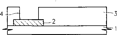
图1A为用于半导体存储器件的一个传统的TFT的平面布局图;
图1B为沿图1A所示a—a线所取的TFT的剖面图;
图2A为本发明的用于半导体存储器件的TFT的平面布局图;
图2B为沿图2A所示a—a线所取的TFT的剖面图;
图3A至3E展示了本发明的用于半导体存储器件的TFT的制造过程。
在说明本发明的实施例前,应先说明一下用于传统的半导体存储器件的TFT。
参照图1A和1B,传统上,在第一绝缘层1上形成多晶硅的第一导电层2的一个图形,作为PMOS TFT的一个漏极接点,然后形成第二绝缘层3。在第二绝缘层3上形成一个开口,即一个通过口或接触口4之后,淀积上非晶硅半导体层5,然后按图形加工。在半导体层5上形成TFT栅极绝缘层6之后,在栅极绝缘层6上淀积多晶硅第二导电层7,然后按图形加工。这样,就形成了TFT的一个栅极电极,与在第二绝缘层3上一个预定区域内的半导体层5重叠。接着,在半导体层5没有被第二导电层7重叠的那部分离子注入或离子射入P型杂质,自我调整,从而形成PMOS TFT的源极和漏极区5a和5b。源极和漏极区5a和5b之间的半导体层作为PMOSTFT的一个沟道区5c。这样,由于为在一个二维平面上形成作为一个传统SRAM负载的PMOS TFT,就应分配一个预定区域,它阻碍了SRAM实现高密度和大容量。
因此,在本发明中,为了减小SRAM的PMOS TFT所占的面积,使用了三维结构。图2A为根据本发明的一个三维TFT的平面布局图,图2B为沿图2A中a—a线所取的一个剖面图。本发明与先有技术的区别在于在PMOS TFT的漏极接触孔内壁上形成的半导体层用作沟道区5c,在接触孔4底部形成的半导体层用作源极区5a。作为栅极的第二导电层7形成的图形还复盖接触孔。并且,通过P型杂质向上扩散来形成源极区5a,即在第一导电层2内置入的第一导电杂质作为源极接点。根据上述结构,PMOS TFT的沟道大小可以调整至接触孔的直径或深度。因此,与传统的PMOSTFT所占的面积相比,面积减小了约40%,而且布线的自由度也大大改善了。
根据本发明的TFT最佳实施例的制造方法由图3A至3E所示的步骤组成。
参照图3A,在一个半导体基片(未示出)上平面化的第一绝缘层1上淀积500至2,000_厚的第一导电层2(例如,多晶硅或非晶硅)。然后,离子注入或射入P型杂质,浓度为1×10¹³~5×10¹⁵/cm2,接着,用普通的光刻法形成第一导电层2的图形。
参照图3B,在第一导电层2的图形上形成2,000至10,000_厚的第二绝缘层3。接着,用普通的光刻法在第一导电层2上的第二绝缘层3内形成一个直径为0.2至0.8μm的接触孔,将第一导电层2暴露出来。
参照图3C,在其中形成了接触孔4的第二绝缘层3上淀积100至1,000_厚的非晶硅半导体层5,然后用普通的光刻法形成半导体层5的图形。接着,用化学汽相淀积法在半导体层5上作为氧化物层涂敷上同样厚度(100到1,000_)的栅极绝缘层6,此时,P型杂质自第一导电层2向上扩散至半导体层5,这样,在半导体层5内形成一个P型杂质区,即源极区5a,并与第一导电层2相接触。
参照图3D,在栅极绝缘层6上淀积500至2,000_厚的第二导电层7(例如,多晶硅或非晶硅),然后,将n型或P型杂质掺入第二导电层7,浓度为1×10¹⁴~1×10¹⁶/cm2,用普通的光刻法形成第二导电层7的图形,作为栅极电极。在去除用以形成第二导电层7图形的光致抗蚀剂8之前,向半导体层5未被第二导电层7重叠的那部分离子注入或射入P型杂质,浓度为1×1013~5×1015/cm2,从而形成一个P型杂质区,即漏极区5b。否则,会如图3D—1所示,在光致抗蚀剂8去除后,形成光致抗蚀剂8a,然后在其内形成一个开口8b。然后,通过开口8b,在半导体层5的预定区域内形成P型杂质区5b′。
参照图3e,去除光致抗蚀剂(8或8a)后,PMOS TFT就完成了。上述PMOS TFT的沟道区5c是作为接触孔4内壁上形成的半导体层和作为未因第二导电层7的图形而注入P型杂质的半导体层来提供的。
如上所述,本发明有一个非晶硅PMOS TFT负载的SRAM的,通过重叠PMOS TFT的源极接触区和作为栅极的第二导电层,接触孔边壁上的半导体层可用作沟道区以形成三维TFT,这样减少了TFT所占用的面积,从而提高了SRAM的密度和容量以及布线的自由度。
尽管参照最佳实施例来具体地展示和说明了本发明,但本领域的技术人员应懂得,在不背离权利要求书所规定的本发明的精神和范围的前提下,可以对其在形式上和细节上做各种不同的改变。
Claims (18)
1.一种用于半导体存储器件的TFT,其特征在于包括:
第一导电层2,它在第一绝缘层1上形成并用第一导电型杂质掺杂;
第二绝缘层3,它覆盖在所说第一导电层2上;
一个开口4,它在所说的第一导电层2上的第二绝缘层3内形成;
一个半导体层5,它在暴露于所说的开口4内的所说的第一导电层2的表面和所说的第二绝缘层3的预定部分的表面上形成;
一个薄栅极绝缘层6,它覆盖在所说的半导体层5上;
第二导电层7,它在所说的开口4里面及其周围的薄栅极绝缘层6上形成;
第一杂质区,它在与所说开口4底部的第一导电层2接触的所说半导体层5的第一部分内形成,并用第一导电型杂质掺杂;
第二杂质区,它在所说第二绝缘层3上的半导体层5的第二部分内形成,并用第一导电型杂质掺杂;以及
一个沟道区5c,它处在所说的半导体层5内的第一与第二杂质区之间。
2.如权利要求1所说的一种用于半导体存储器件的TFT,其特征在于所说的沟道区5c的大小由所说开口4的直径或深度来决定。
3.如权利要求1所说的一种用于半导体存储器件的TFT,其特征在于所说的第一导电型杂质为P型。
4.如权利要求1所说的一种用于半导体存储器件的TFT,其特征在于所说的第一杂质区的杂质自所说的第一导电层2向上扩散。
5.一种用于半导体存储器件的TFT的制造方法,其特征在于包括以下步骤:
在第一绝缘层1上形成用第一导电型杂质掺杂的第一导电层2;
用第二绝缘层3覆盖所说的第一导电层2;
在所说的第一导电层2上的第二绝缘层3内形成一个开口4;
在暴露于所说开口4内的第一导电层2的表面和所说第二绝缘层3的预定部分的表面上形成一个半导体层5;
用薄栅极绝缘层6覆盖所说的半导体层5,并同时通过向上扩散所说第一导电层2内的杂质,在与所说暴露的第一导电层2接触的半导体层5的第一部分内形成第一杂质区;
在所说的开口4里面和周围的薄栅极绝缘层6上形成第二导电层7;以及
通过掺杂工艺在所说半导体层5的第二部分形成第二杂质区,它不盖所说第二绝缘层3上的第二导电层7。
6.如权利要求5所说的一种用于半导体存储器件的TFT的制造方法,其特征在于所说的第一导电层2为掺有P型杂质的多晶硅。
7.如权利要求5所说的一种用于半导体存储器件的TFT的制造方法,其特征在于所说的第一导电层2为掺有P型杂质的非晶硅。
8.如权利要求5所说的一种用于半导体存储器件TFT的制造方法,其特征在于所说第一导电层2的杂质浓度为1×10¹³~5×10¹⁵/cm2。
9.如权利要求5所说的一种用于半导体存储器件的TFT的制造方法,其特征在于所说的第二绝缘层3的厚度为2,000至10,000_。
10.如权利要求5所说的一种用于半导体存储器件的TFT的制造方法,其特征在于所说的开口4的直径为0.2~0.8μm。
11.如权利要求5所说的一种用于半导体存储器件的TFT的制造方法,其特征在于所说的半导体层5为100至1,500_厚,并由非晶硅制成。
12.如权利要求5所说的一种用于半导体存储器件TFT的制造方法,其特征在于所说的栅极绝缘层6的厚度为100至1,000_。
13.如权利要求5所说的一种用于半导体存储器件的TFT的制造方法,其特征在于所说的第二导电层7为掺有n型杂质的多晶硅。
14.如权利要求5所说的一种用于半导体存储器件的TFT的制造方法,其特征在于所说半导体层5中的杂质区的杂质浓度为1×10¹³~5×10¹⁵/cm/2。
15.如权利要求5所说的一种用于半导体存储器件的TFT的制造方法,其特征在于所说的第二导电层7为掺有P型杂质的多晶硅。
16.如权利要求5所说的一种用于半导体存储器件的TFT的制造方法,其特征在于所说的第二导电层7为非晶硅。
17.如权利要求5所说的一种用于半导体存储器件的TFT的制造方法,其特征在于所说的掺杂过程是用所说的第二导电层7作为掩模进行离子注入。
18.如权利要求5所说的一种用于半导体存储器件的TFT的制造方法,其特征在于所说的掺杂过程是用一个预定的光致抗蚀剂图形作为掩模进行离子注入。
Applications Claiming Priority (6)
| Application Number | Priority Date | Filing Date | Title |
|---|---|---|---|
| KR24664/91 | 1991-12-27 | ||
| KR91-24664 | 1991-12-27 | ||
| KR910024664 | 1991-12-27 | ||
| KR6678/92 | 1992-04-21 | ||
| KR92-6678 | 1992-04-21 | ||
| KR1019920006678A KR950001159B1 (ko) | 1991-12-27 | 1992-04-21 | 반도체 메모리장치의 박막트랜지스터 및 그 제조방법 |
Publications (2)
| Publication Number | Publication Date |
|---|---|
| CN1073806A CN1073806A (zh) | 1993-06-30 |
| CN1032286C true CN1032286C (zh) | 1996-07-10 |
Family
ID=26628882
Family Applications (1)
| Application Number | Title | Priority Date | Filing Date |
|---|---|---|---|
| CN92105269A Expired - Lifetime CN1032286C (zh) | 1991-12-27 | 1992-06-30 | 用于半导体存储器件的薄膜晶体管及其制造方法 |
Country Status (9)
| Country | Link |
|---|---|
| US (1) | US5270968A (zh) |
| JP (1) | JPH0773114B2 (zh) |
| KR (1) | KR950001159B1 (zh) |
| CN (1) | CN1032286C (zh) |
| DE (1) | DE4221420A1 (zh) |
| FR (1) | FR2685818B1 (zh) |
| GB (1) | GB2262838B (zh) |
| IT (1) | IT1255398B (zh) |
| TW (1) | TW212851B (zh) |
Cited By (1)
| Publication number | Priority date | Publication date | Assignee | Title |
|---|---|---|---|---|
| CN100409425C (zh) * | 1997-04-04 | 2008-08-06 | 格伦·J·利迪 | 三维结构存储器的制造方法及使用方法 |
Families Citing this family (18)
| Publication number | Priority date | Publication date | Assignee | Title |
|---|---|---|---|---|
| US5418393A (en) * | 1993-11-29 | 1995-05-23 | Motorola, Inc. | Thin-film transistor with fully gated channel region |
| US5700727A (en) * | 1995-07-24 | 1997-12-23 | Micron Technology, Inc. | Method of forming a thin film transistor |
| KR100223886B1 (ko) * | 1995-12-26 | 1999-10-15 | 구본준 | 반도체소자 및 제조방법 |
| US6238971B1 (en) | 1997-02-11 | 2001-05-29 | Micron Technology, Inc. | Capacitor structures, DRAM cell structures, and integrated circuitry, and methods of forming capacitor structures, integrated circuitry and DRAM cell structures |
| US5981333A (en) * | 1997-02-11 | 1999-11-09 | Micron Technology, Inc. | Methods of forming capacitors and DRAM arrays |
| US5918122A (en) * | 1997-02-11 | 1999-06-29 | Micron Technology, Inc. | Methods of forming integrated circuitry, DRAM cells and capacitors |
| US6214727B1 (en) * | 1997-02-11 | 2001-04-10 | Micron Technology, Inc. | Conductive electrical contacts, capacitors, DRAMs, and integrated circuitry, and methods of forming conductive electrical contacts, capacitors, DRAMs, and integrated circuitry |
| US5905280A (en) | 1997-02-11 | 1999-05-18 | Micron Technology, Inc. | Capacitor structures, DRAM cell structures, methods of forming capacitors, methods of forming DRAM cells, and integrated circuits incorporating capacitor structures and DRAM cell structures |
| KR100259078B1 (ko) | 1997-08-14 | 2000-06-15 | 김영환 | 박막트랜지스터 및 이의 제조방법 |
| US6359302B1 (en) | 1997-10-16 | 2002-03-19 | Micron Technology, Inc. | DRAM cells and integrated circuitry, and capacitor structures |
| TW400644B (en) * | 1998-10-26 | 2000-08-01 | United Microelectronics Corp | The structure of Dynamic Random Access Memory(DRAM) and the manufacture method thereof |
| GB2362755A (en) * | 2000-05-25 | 2001-11-28 | Nanogate Ltd | Thin film field effect transistor with a conical structure |
| KR100411813B1 (ko) * | 2001-10-11 | 2003-12-24 | 한국전력공사 | 유동제어를 이용한 축열식 전기온돌의 실내온도조절시스템 |
| KR100670140B1 (ko) * | 2004-08-26 | 2007-01-16 | 삼성에스디아이 주식회사 | 커패시터 |
| TWI552345B (zh) * | 2011-01-26 | 2016-10-01 | 半導體能源研究所股份有限公司 | 半導體裝置及其製造方法 |
| CN104795400B (zh) * | 2015-02-12 | 2018-10-30 | 合肥鑫晟光电科技有限公司 | 阵列基板制造方法、阵列基板和显示装置 |
| CN114005838B (zh) * | 2021-10-22 | 2024-02-09 | 武汉华星光电技术有限公司 | 一种阵列基板和显示面板 |
| WO2023175437A1 (ja) * | 2022-03-18 | 2023-09-21 | 株式会社半導体エネルギー研究所 | 半導体装置、及び、半導体装置の作製方法 |
Family Cites Families (6)
| Publication number | Priority date | Publication date | Assignee | Title |
|---|---|---|---|---|
| JPS59208783A (ja) * | 1983-05-12 | 1984-11-27 | Seiko Instr & Electronics Ltd | 薄膜トランジスタ |
| JPS601868A (ja) * | 1983-06-17 | 1985-01-08 | Seiko Instr & Electronics Ltd | 薄膜トランジスタ |
| US4820652A (en) * | 1985-12-11 | 1989-04-11 | Sony Corporation | Manufacturing process and structure of semiconductor memory devices |
| GB2201544A (en) * | 1987-02-27 | 1988-09-01 | Philips Electronic Associated | Vertical thin film transistor |
| JPH01231376A (ja) * | 1988-03-11 | 1989-09-14 | Nec Corp | 薄膜トランジスタおよびその製造方法 |
| US5210429A (en) * | 1990-06-29 | 1993-05-11 | Sharp Kabushiki Kaisha | Static RAM cell with conductive straps formed integrally with thin film transistor gates |
-
1992
- 1992-04-21 KR KR1019920006678A patent/KR950001159B1/ko not_active IP Right Cessation
- 1992-06-23 FR FR9207651A patent/FR2685818B1/fr not_active Expired - Lifetime
- 1992-06-29 GB GB9213809A patent/GB2262838B/en not_active Expired - Lifetime
- 1992-06-30 DE DE4221420A patent/DE4221420A1/de not_active Withdrawn
- 1992-06-30 TW TW081105179A patent/TW212851B/zh active
- 1992-06-30 US US07/906,369 patent/US5270968A/en not_active Expired - Lifetime
- 1992-06-30 CN CN92105269A patent/CN1032286C/zh not_active Expired - Lifetime
- 1992-06-30 IT ITMI921603A patent/IT1255398B/it active IP Right Grant
- 1992-07-14 JP JP4187031A patent/JPH0773114B2/ja not_active Expired - Fee Related
Cited By (1)
| Publication number | Priority date | Publication date | Assignee | Title |
|---|---|---|---|---|
| CN100409425C (zh) * | 1997-04-04 | 2008-08-06 | 格伦·J·利迪 | 三维结构存储器的制造方法及使用方法 |
Also Published As
| Publication number | Publication date |
|---|---|
| TW212851B (zh) | 1993-09-11 |
| FR2685818B1 (fr) | 1994-04-15 |
| CN1073806A (zh) | 1993-06-30 |
| ITMI921603A1 (it) | 1993-12-30 |
| JPH0653440A (ja) | 1994-02-25 |
| IT1255398B (it) | 1995-10-31 |
| KR930015098A (ko) | 1993-07-23 |
| JPH0773114B2 (ja) | 1995-08-02 |
| US5270968A (en) | 1993-12-14 |
| DE4221420A1 (de) | 1993-07-01 |
| KR950001159B1 (ko) | 1995-02-11 |
| FR2685818A1 (fr) | 1993-07-02 |
| GB9213809D0 (en) | 1992-08-12 |
| ITMI921603A0 (it) | 1992-06-30 |
| GB2262838A (en) | 1993-06-30 |
| GB2262838B (en) | 1995-09-06 |
Similar Documents
| Publication | Publication Date | Title |
|---|---|---|
| CN1032286C (zh) | 用于半导体存储器件的薄膜晶体管及其制造方法 | |
| CN1103123C (zh) | 引入堆叠箱式电容单元的数兆位动态存储器的劈开-多晶硅cmos工艺 | |
| US5668391A (en) | Vertical thin film transistor | |
| US5716879A (en) | Method of making a thin film transistor | |
| US5716862A (en) | High performance PMOSFET using split-polysilicon CMOS process incorporating advanced stacked capacitior cells for fabricating multi-megabit DRAMS | |
| US5478768A (en) | Method of manufacturing a semiconductor memory device having improved hold characteristic of a storage capacitor | |
| US5262655A (en) | Thin film field effect device having an LDD structure and a method of manufacturing such a device | |
| CN1088914C (zh) | 制造金属氧化物半导体场效应晶体管的方法 | |
| JPH07211799A (ja) | Dramセルの製造方法 | |
| US6458665B1 (en) | Halo ion implantation method for fabricating a semiconductor device | |
| US5659183A (en) | Thin film transistor having a drain offset region | |
| KR960006718B1 (ko) | 반도체 기억장치의 커패시터 및 그 제조방법 | |
| CN1135615C (zh) | 半导体器件制造方法 | |
| US6200839B1 (en) | Methods of forming thin film transistors | |
| JPH03268462A (ja) | メモリセルを作成する方法 | |
| US5646061A (en) | Two-layer polysilicon process for forming a stacked DRAM capacitor with improved doping uniformity and a controllable shallow junction contact | |
| US5343062A (en) | Semiconductor memory having a memory cell including a capacitor with a two-layer lower electrode | |
| JPH05267678A (ja) | 半導体装置およびその製造方法 | |
| CN1186821C (zh) | 双垂直通道薄膜晶体管及其制造方法 | |
| CN1053996C (zh) | 一种制作动态随机存取存储器的方法 | |
| KR100218330B1 (ko) | 노아형 마스크 롬 및 그의 제조방법 | |
| KR100265677B1 (ko) | 반도체 장치 및 그의 제조 공정 | |
| KR930003859B1 (ko) | 반도체장치의 제조방법 | |
| KR930011544B1 (ko) | 적층형 셀 제조방법 | |
| KR960013637B1 (ko) | 디램 셀의 구조 및 그 제조방법 |
Legal Events
| Date | Code | Title | Description |
|---|---|---|---|
| C06 | Publication | ||
| PB01 | Publication | ||
| C10 | Entry into substantive examination | ||
| SE01 | Entry into force of request for substantive examination | ||
| C14 | Grant of patent or utility model | ||
| GR01 | Patent grant | ||
| C15 | Extension of patent right duration from 15 to 20 years for appl. with date before 31.12.1992 and still valid on 11.12.2001 (patent law change 1993) | ||
| OR01 | Other related matters | ||
| C17 | Cessation of patent right | ||
| CX01 | Expiry of patent term |
Expiration termination date: 20120630 Granted publication date: 19960710 |