WO2024204537A1 - 半導体装置および半導体装置の製造方法 - Google Patents
半導体装置および半導体装置の製造方法 Download PDFInfo
- Publication number
- WO2024204537A1 WO2024204537A1 PCT/JP2024/012641 JP2024012641W WO2024204537A1 WO 2024204537 A1 WO2024204537 A1 WO 2024204537A1 JP 2024012641 W JP2024012641 W JP 2024012641W WO 2024204537 A1 WO2024204537 A1 WO 2024204537A1
- Authority
- WO
- WIPO (PCT)
- Prior art keywords
- layer
- insulating layer
- electron supply
- electron
- semiconductor device
- Prior art date
- Legal status (The legal status is an assumption and is not a legal conclusion. Google has not performed a legal analysis and makes no representation as to the accuracy of the status listed.)
- Ceased
Links
Images






Classifications
-
- H—ELECTRICITY
- H10—SEMICONDUCTOR DEVICES; ELECTRIC SOLID-STATE DEVICES NOT OTHERWISE PROVIDED FOR
- H10D—INORGANIC ELECTRIC SEMICONDUCTOR DEVICES
- H10D64/00—Electrodes of devices having potential barriers
- H10D64/118—Electrodes comprising insulating layers having particular dielectric or electrostatic properties, e.g. having static charges
-
- H—ELECTRICITY
- H10—SEMICONDUCTOR DEVICES; ELECTRIC SOLID-STATE DEVICES NOT OTHERWISE PROVIDED FOR
- H10D—INORGANIC ELECTRIC SEMICONDUCTOR DEVICES
- H10D30/00—Field-effect transistors [FET]
- H10D30/40—FETs having zero-dimensional [0D], one-dimensional [1D] or two-dimensional [2D] charge carrier gas channels
- H10D30/47—FETs having zero-dimensional [0D], one-dimensional [1D] or two-dimensional [2D] charge carrier gas channels having two-dimensional [2D] charge carrier gas channels, e.g. nanoribbon FETs or high electron mobility transistors [HEMT]
- H10D30/471—High electron mobility transistors [HEMT] or high hole mobility transistors [HHMT]
- H10D30/475—High electron mobility transistors [HEMT] or high hole mobility transistors [HHMT] having wider bandgap layer formed on top of lower bandgap active layer, e.g. undoped barrier HEMTs such as i-AlGaN/GaN HEMTs
- H10D30/4755—High electron mobility transistors [HEMT] or high hole mobility transistors [HHMT] having wider bandgap layer formed on top of lower bandgap active layer, e.g. undoped barrier HEMTs such as i-AlGaN/GaN HEMTs having wide bandgap charge-carrier supplying layers, e.g. modulation doped HEMTs such as n-AlGaAs/GaAs HEMTs
-
- H—ELECTRICITY
- H10—SEMICONDUCTOR DEVICES; ELECTRIC SOLID-STATE DEVICES NOT OTHERWISE PROVIDED FOR
- H10D—INORGANIC ELECTRIC SEMICONDUCTOR DEVICES
- H10D30/00—Field-effect transistors [FET]
- H10D30/01—Manufacture or treatment
- H10D30/015—Manufacture or treatment of FETs having heterojunction interface channels or heterojunction gate electrodes, e.g. HEMT
-
- H—ELECTRICITY
- H10—SEMICONDUCTOR DEVICES; ELECTRIC SOLID-STATE DEVICES NOT OTHERWISE PROVIDED FOR
- H10D—INORGANIC ELECTRIC SEMICONDUCTOR DEVICES
- H10D30/00—Field-effect transistors [FET]
- H10D30/40—FETs having zero-dimensional [0D], one-dimensional [1D] or two-dimensional [2D] charge carrier gas channels
- H10D30/47—FETs having zero-dimensional [0D], one-dimensional [1D] or two-dimensional [2D] charge carrier gas channels having two-dimensional [2D] charge carrier gas channels, e.g. nanoribbon FETs or high electron mobility transistors [HEMT]
- H10D30/471—High electron mobility transistors [HEMT] or high hole mobility transistors [HHMT]
- H10D30/475—High electron mobility transistors [HEMT] or high hole mobility transistors [HHMT] having wider bandgap layer formed on top of lower bandgap active layer, e.g. undoped barrier HEMTs such as i-AlGaN/GaN HEMTs
-
- H—ELECTRICITY
- H10—SEMICONDUCTOR DEVICES; ELECTRIC SOLID-STATE DEVICES NOT OTHERWISE PROVIDED FOR
- H10D—INORGANIC ELECTRIC SEMICONDUCTOR DEVICES
- H10D62/00—Semiconductor bodies, or regions thereof, of devices having potential barriers
- H10D62/10—Shapes, relative sizes or dispositions of the regions of the semiconductor bodies; Shapes of the semiconductor bodies
- H10D62/117—Shapes of semiconductor bodies
-
- H—ELECTRICITY
- H10—SEMICONDUCTOR DEVICES; ELECTRIC SOLID-STATE DEVICES NOT OTHERWISE PROVIDED FOR
- H10D—INORGANIC ELECTRIC SEMICONDUCTOR DEVICES
- H10D62/00—Semiconductor bodies, or regions thereof, of devices having potential barriers
- H10D62/10—Shapes, relative sizes or dispositions of the regions of the semiconductor bodies; Shapes of the semiconductor bodies
- H10D62/13—Semiconductor regions connected to electrodes carrying current to be rectified, amplified or switched, e.g. source or drain regions
- H10D62/149—Source or drain regions of field-effect devices
- H10D62/161—Source or drain regions of field-effect devices of FETs having Schottky gates
-
- H—ELECTRICITY
- H10—SEMICONDUCTOR DEVICES; ELECTRIC SOLID-STATE DEVICES NOT OTHERWISE PROVIDED FOR
- H10D—INORGANIC ELECTRIC SEMICONDUCTOR DEVICES
- H10D64/00—Electrodes of devices having potential barriers
- H10D64/20—Electrodes characterised by their shapes, relative sizes or dispositions
- H10D64/23—Electrodes carrying the current to be rectified, amplified, oscillated or switched, e.g. sources, drains, anodes or cathodes
- H10D64/251—Source or drain electrodes for field-effect devices
- H10D64/256—Source or drain electrodes for field-effect devices for lateral devices wherein the source or drain electrodes are recessed in semiconductor bodies
-
- H—ELECTRICITY
- H10—SEMICONDUCTOR DEVICES; ELECTRIC SOLID-STATE DEVICES NOT OTHERWISE PROVIDED FOR
- H10D—INORGANIC ELECTRIC SEMICONDUCTOR DEVICES
- H10D64/00—Electrodes of devices having potential barriers
- H10D64/60—Electrodes characterised by their materials
-
- H—ELECTRICITY
- H10—SEMICONDUCTOR DEVICES; ELECTRIC SOLID-STATE DEVICES NOT OTHERWISE PROVIDED FOR
- H10D—INORGANIC ELECTRIC SEMICONDUCTOR DEVICES
- H10D62/00—Semiconductor bodies, or regions thereof, of devices having potential barriers
- H10D62/80—Semiconductor bodies, or regions thereof, of devices having potential barriers characterised by the materials
- H10D62/85—Semiconductor bodies, or regions thereof, of devices having potential barriers characterised by the materials being Group III-V materials, e.g. GaAs
- H10D62/8503—Nitride Group III-V materials, e.g. AlN or GaN
-
- H—ELECTRICITY
- H10—SEMICONDUCTOR DEVICES; ELECTRIC SOLID-STATE DEVICES NOT OTHERWISE PROVIDED FOR
- H10D—INORGANIC ELECTRIC SEMICONDUCTOR DEVICES
- H10D64/00—Electrodes of devices having potential barriers
- H10D64/111—Field plates
- H10D64/112—Field plates comprising multiple field plate segments
-
- H—ELECTRICITY
- H10—SEMICONDUCTOR DEVICES; ELECTRIC SOLID-STATE DEVICES NOT OTHERWISE PROVIDED FOR
- H10D—INORGANIC ELECTRIC SEMICONDUCTOR DEVICES
- H10D64/00—Electrodes of devices having potential barriers
- H10D64/20—Electrodes characterised by their shapes, relative sizes or dispositions
- H10D64/23—Electrodes carrying the current to be rectified, amplified, oscillated or switched, e.g. sources, drains, anodes or cathodes
- H10D64/251—Source or drain electrodes for field-effect devices
Definitions
- one aspect of the first manufacturing method of the semiconductor device includes the steps of forming an electron supply layer on an electron transit layer, the electron supply layer having a band gap larger than that of the electron transit layer, forming an insulating layer containing Si on the electron supply layer without exposing it to the atmosphere, thinning a part of the insulating layer to form a thin portion in the insulating layer, forming a through recess that penetrates the thin portion of the insulating layer and the electron supply layer and reaches the electron transit layer while leaving a part of the thin portion as an insulating layer remnant, embedding a contact layer in the through recess, forming a source electrode and/or a drain electrode across the insulating layer remnant and the contact layer, forming an alloy layer and an electron supply auxiliary layer in the insulating layer remnant and the electron supply layer by heat treatment, and removing the insulating layer from a portion of the insulating layer that is separated from the source electrode and/or the drain electrode to form a gate electrode.
- Fig. 1 is a cross-sectional view showing the configuration of the semiconductor device 1 according to the first embodiment.
- the semiconductor device 1 is a high electron mobility transistor (HEMT) with a Schottky junction gate structure.
- HEMT high electron mobility transistor
- the semiconductor device 1 includes a substrate 101, a buffer layer 102, an electron transit layer 103, an electron supply layer 104, a first insulating layer 201, a second insulating layer 202, a source electrode 301, a drain electrode 302, a gate electrode 303, an electron supply auxiliary layer 401, and an alloy layer 402.
- the substrate 101 is, for example, a silicon substrate made of Si.
- the substrate 101 is, for example, a silicon substrate made of single crystal Si with a (111) principal surface.
- the substrate 101 is not limited to a silicon substrate, and may be a substrate made of sapphire, SiC, GaN, AlN, or the like, which serves as a base for forming a nitride semiconductor layer.
- the resistivity of the substrate 101 is, for example, 1 k ⁇ or more.
- the substrate 101 may have a resistivity of 20 ⁇ or less.
- the buffer layer 102 is provided on the substrate 101.
- the buffer layer 102 is, for example, a 2 ⁇ m thick Group III nitride semiconductor layer made of a multi-layer structure of AlN and AlGaN. In this case, 20 to 100 pairs of AlN and AlGaN may be laminated.
- the buffer layer 102 may have a structure in which a multi-layer of Al 1- ⁇ Ga ⁇ N (0 ⁇ 0.8) layers is laminated, and may include a superlattice structure.
- the buffer layer 102 may be made of a single layer or multiple layers of Group III nitride semiconductors such as InGaN and AlInGaN.
- the carbon concentration of the buffer layer 102 may be set to 1 ⁇ 10 19 atoms/cm 3 or more to increase the resistance of the buffer layer 102.
- the electron transit layer 103 is provided on the buffer layer 102.
- the electron transit layer 103 is, for example, a GaN layer made of GaN with a thickness of 150 nm.
- the group III nitride semiconductor that makes up the electron transit layer 103 is not limited to GaN.
- the electron transit layer 103 may be made of a group III nitride semiconductor such as InGaN, AlGaN, or AlInGaN.
- the electron transit layer 103 may also contain n-type impurities.
- the electron supply layer 104 is provided on the electron transit layer 103.
- the electron supply layer 104 has a larger band gap than the electron transit layer 103.
- the electron supply layer 104 is, for example, an AlGaN layer having a thickness of 13 nm and made of AlGaN with an Al composition ratio of 30%.
- a high concentration of two-dimensional electron gas is generated on the electron transit layer 103 side of the heterointerface between the electron supply layer 104 and the electron transit layer 103, and a channel of the two-dimensional electron gas layer 105 is formed. Therefore, the semiconductor device 1 has a two-dimensional electron gas layer 105.
- the two-dimensional electron gas layer 105 is composed of a first two-dimensional electron gas layer 105A and a second two-dimensional electron gas layer 105B having different electron concentrations of the two-dimensional electron gas.
- the Al composition ratio of the electron supply layer 104 made of AlGaN is not limited to 30%.
- the Al composition ratio of the electron supply layer 104 may be 20 to 100%.
- the group III nitride semiconductor constituting the electron supply layer 104 is not limited to AlGaN.
- the electron supply layer 104 may be composed of a group III nitride semiconductor containing In, such as AlInGaN.
- the electron supply layer 104 may contain n-type impurities.
- a cap layer may be provided on the electron supply layer 104.
- the cap layer may be, for example, a GaN layer made of GaN and having a thickness of about 1 to 2 nm.
- a spacer layer may be provided between the electron transit layer 103 and the electron supply layer 104.
- the spacer layer may be, for example, an AlN layer made of AlN and having a thickness of about 1 nm.
- the first insulating layer 201 is provided on the electron supply layer 104.
- the first insulating layer 201 is an insulating layer containing Si (silicon).
- the first insulating layer 201 is a SiN layer made of SiN.
- the first insulating layer 201 is a SiN layer made of in-situ SiN and has a thickness of 2 nm. Note that "in-situ” means that it is formed without exposure to the atmosphere. Therefore, the first insulating layer 201 made of in-situ SiN is a SiN layer formed without exposure to the atmosphere after the electron supply layer 104 is formed.
- the first insulating layer 201 By forming the first insulating layer 201 from In-situ SiN in this way, it is possible to eliminate uneven distribution of oxygen at the interface between the first insulating layer 201 and the electron supply layer 104. By eliminating uneven distribution of oxygen at the interface between the first insulating layer 201 and the electron supply layer 104, the occurrence of interface states is suppressed. This makes it possible to avoid an increase in the potential at the interface and suppress a decrease in the electron concentration of the two-dimensional electron gas.
- the thickness of the first insulating layer 201 is preferably 2 nm or more and 30 nm or less. By making the thickness of the first insulating layer 201 2 nm or more, it is possible to suppress uneven distribution of oxygen at the interface between the first insulating layer 201 and the electron supply layer 104 due to natural oxidation. On the other hand, if the thickness of the first insulating layer 201 exceeds 30 nm, the wafer will warp when the semiconductor device 1 is manufactured, and the quality of the semiconductor device 1 will deteriorate. For this reason, it is preferable that the thickness of the first insulating layer 201 is 30 nm or less. In other words, by making the thickness of the first insulating layer 201 30 nm or less, it is possible to suppress warping of the wafer.
- the first insulating layer 201 does not contain oxygen. If the first insulating layer 201 contains oxygen, the interface state at the interface between the first insulating layer 201 and the electron supply layer 104 increases, the potential at the interface between the first insulating layer 201 and the electron supply layer 104 increases, and the electron concentration of the two-dimensional electron gas decreases. By not including oxygen in the first insulating layer 201, it is possible to suppress a decrease in the electron concentration of the two-dimensional electron gas.
- the second insulating layer 202 is provided on the first insulating layer 201.
- the second insulating layer 202 is in contact with the first insulating layer 201.
- the thickness of the second insulating layer 202 is thicker than that of the first insulating layer 201, but is not limited thereto. That is, the thickness of the second insulating layer 202 may be thinner than that of the first insulating layer 201.
- the second insulating layer 202 is, for example, a silicon oxide layer made of SiO 2 and having a thickness of 50 nm. Note that the second insulating layer 202 is not limited to SiO 2 , and may be made of SiN, SiON, or the like.
- the first insulating layer 201 has an opening 201a.
- the opening 201a is formed in the first insulating layer 201 in a region where the gate electrode 303 is provided. Therefore, the first insulating layer 201 is provided on a portion of the electron supply layer 104 where the gate electrode 303 is not provided.
- the second insulating layer 202 also has an opening 202a.
- the opening 202a is formed in the second insulating layer 202 in a region where the gate electrode 303 is provided. Therefore, the second insulating layer 202 is provided on a portion of the first insulating layer 201 where the gate electrode 303 is not provided.
- the first insulating layer 201 and the second insulating layer 202 are in contact with the gate electrode 303.
- the first insulating layer 201 and the second insulating layer 202 are not in contact with the contact layer 212.
- the first insulating layer 201 and the second insulating layer 202 are not in contact with either the source side contact layer 212A or the drain side contact layer 212B, but this is not limited to the above.
- the first insulating layer 201 may not be in contact with either the source side contact layer 212A or the drain side contact layer 212B, but may be in contact with the other.
- the second insulating layer 202 may not be in contact with either the source side contact layer 212A or the drain side contact layer 212B, but may be in contact with the other.
- the electron supply layer 104 is provided with a through recess 211.
- the through recess 211 is provided so as to penetrate through the first insulating layer 201 and the electron supply layer 104 and reach the electron transit layer 103.
- the through recess 211 reaches the inside of the electron transit layer 103, and a recess is provided in the electron transit layer 103.
- the distance from the top surface of the electron transit layer 103 to the bottommost part of the bottom surface of the through recess 211 is preferably 10 nm or less. As an example, the distance from the top surface of the electron transit layer 103 to the bottommost part of the bottom surface of the through recess 211 is 5 nm.
- the angle of elevation from the center to the side at the bottom surface of the through recess 211 is preferably 10 degrees or less, and more preferably 5 degrees or less. In this way, it is possible to reduce the occurrence of crystal defects on the side surface of the through recess 211 when the through recess 211 is formed by dry etching, and to suppress a decrease in the maximum drain current.
- the through recess portion 211 is provided in a region corresponding to the region in which the source electrode 301 and the drain electrode 302 are provided. Specifically, the through recess portion 211 is provided in a pair so as to face each other with the gate electrode 303 in between.
- a contact layer 212 is provided in the through recess 211.
- the contact layer 212 is provided so as to fill the through recess 211.
- the contact layer 212 provided in one of the pair of through recesses 211 is a source side contact layer 212A
- the contact layer 212 provided in the other of the pair of through recesses 211 is a drain side contact layer 212B.
- the source side contact layer 212A and the drain side contact layer 212B are provided at positions sandwiching the gate electrode 303.
- the through recess 211 is provided at a distance from the first insulating layer 201 and the second insulating layer 202. Therefore, the contact layer 212 embedded in the through recess 211 is also at a distance from the first insulating layer 201 and the second insulating layer 202, and the contact layer 212 is not in contact with the first insulating layer 201 and the second insulating layer 202.
- the contact layer 212 is, for example, an n-GaN layer made of n-type GaN.
- the material constituting the contact layer 212 is not limited to n-type GaN, and may be a group III nitride semiconductor such as InGaN, AlGaN, or AlInGaN that contains donors such as Si or Ge as n-type impurities, or may be a multilayer electrode film having a layered structure in which Ti and Al are stacked in order.
- the material constituting the contact layer 212 may also be composed of Ti, Ta, Al, Au, Hf, Ru, and Cu.
- a source electrode 301 or a drain electrode 302 is provided on the contact layer 212. Specifically, the source electrode 301 is provided on the source side contact layer 212A, and the drain electrode 302 is provided on the drain side contact layer 212B. The source electrode 301 and the drain electrode 302 are provided so as to face each other with the gate electrode 303 interposed therebetween.
- the source electrode 301 and the drain electrode 302 are also provided on the contact layer 212 and the alloy layer 402.
- the source electrode 301 and the drain electrode 302 also cover a part of the second insulating layer 202.
- the source electrode 301 is provided so as to cover the source side contact layer 212A, the alloy layer 402, and a part of the second insulating layer 202.
- the drain electrode 302 is provided so as to cover the drain side contact layer 212B, the alloy layer 402, and a part of the second insulating layer 202.
- the source electrode 301 and the drain electrode 302 are formed, for example, by a multilayer electrode film having a laminated structure in which a Ti film having a thickness of 30 nm and an Al film having a thickness of 200 nm are laminated in this order, but are not limited to this.
- the source electrode 301 and the drain electrode 302 may also be formed using Ti, Ta, W, Al, Au, Hf, Ru, and Cu.
- the gate electrode 303 is provided on the electron supply layer 104. Specifically, the gate electrode 303 is provided on the electron supply layer 104 via an opening 201a provided in the first insulating layer 201 and an opening 202a provided in the second insulating layer 202. Note that the opening width of the opening 201a in the first insulating layer 201 and the opening width of the opening 202a in the second insulating layer 202 are the same, but are not limited to this.
- the gate electrode 303 is, for example, a multilayer electrode film having a laminated structure in which a TiN film and an Al film are laminated in order.
- the gate electrode 303 is not limited to a laminated structure of a TiN film and an Al film, and may be composed of a nitride and a carbide of a transition metal.
- the gate electrode 303 may be composed of TiN, WN, TaN, or HfN.
- the gate electrode 303 may be composed of Ti, Ta, W, Al, Pd, Pt, Hf, Ru, or Cu, or may be a compound containing these elements, or may be a multilayer electrode film having a laminated structure.
- Another insulating layer or a p-type nitride semiconductor layer may be provided between the electron supply layer 104 and the gate electrode 303.
- the electron supply assist layer 401 is an n-type semiconductor layer made of an n-type semiconductor containing Si.
- the thickness of the electron supply assist layer 401 is preferably 2 nm or less, but is not limited to this.
- the electron supply assist layer 401 is an n-AlGaN layer made of n-type AlGaN containing Si and having a thickness of 1 nm.
- the electron supply assist layer 401 is not in contact with the gate electrode 303, but is in contact with the electron supply layer 104 and the contact layer 212.
- the electron supply assist layer 401 is provided between the contact layer 212 and the first insulating layer 201.
- the electron supply assist layer 401 is provided so as to be embedded in the end of the electron supply layer 104 on the contact layer 212 side.
- the electron supply assist layer 401 is provided so that its upper surface is flush with the upper surface of the electron supply layer 104 and its lower surface is located between the upper and lower surfaces of the electron supply layer 104.
- the electron supply assist layer 401 is in contact with each of the source side contact layer 212A and the drain side contact layer 212B. Specifically, the electron supply assist layer 401 is embedded in the end of the electron supply layer 104 on the source side contact layer 212A side and is embedded in the end of the electron supply layer 104 on the drain side contact layer 212B side. The electron supply assist layer 401 may be in contact with only one of the source side contact layer 212A and the drain side contact layer 212B. The electron supply assist layer 401 may be divided into a plurality of layers.
- the electron supply assist layer 401 on the source electrode 301 side of the plurality of electron supply assist layers 401 may be in contact with the source side contact layer 212A, and the electron supply assist layer 401 on the drain electrode 302 side of the plurality of electron supply assist layers 401 may be in contact with the drain side contact layer 212B.
- the width of the electron supply assist layer 401 may be smaller than the distance L between the end of the electron supply assist layer 401 on the gate electrode 303 side and the gate electrode 303.
- the width of the electron supply assist layer 401 is 1 ⁇ m or less in a cross-sectional view. In this way, an increase in leakage current between the gate electrode 303 and the drain electrode 302 can be efficiently suppressed.
- one of the electron supply assist layer 401 on the source electrode 301 side and the electron supply assist layer 401 on the drain electrode 302 side may not be in contact with the gate electrode 303, and the other may be in contact with the gate electrode 303.
- the electron supply assist layer 401 on the drain electrode 302 side may be in contact with the gate electrode 303. In this way, the access resistance between the source electrode 301 and the gate electrode 303 can be reduced, and the maximum drain current can be increased.
- the alloy layer 402 is provided on the electron supply assist layer 401, which is an n-type semiconductor layer. Specifically, the alloy layer 402 is provided directly on the electron supply assist layer 401 and is in contact with the electron supply assist layer 401.
- the alloy layer 402 is a Si-based alloy layer containing Si.
- the alloy layer 402 is an alloy layer formed by a reaction between an element constituting the first insulating layer 201 and an element constituting the source electrode 301 and/or the drain electrode 302.
- the Si constituting the alloy layer 402 is derived from the Si contained in the first insulating layer 201.
- the first insulating layer 201 is a SiN layer, and the source electrode 301 and the drain electrode 302 are laminated films of a Ti film and an Al film, so the alloy layer 402 is an alloy layer composed of Ti, Al, Si, and N.
- the alloy layer 402 is a TiAlSiN alloy layer composed of a TiAlSiN alloy and has a thickness of 1 nm.
- the thickness of the alloy layer 402 is not limited to 1 nm, but is preferably 2 nm or less. In this way, the concentration of Si diffusing into the electron supply layer 104 can be increased.
- the alloy constituting the alloy layer 402 is not limited to a TiAlSiN alloy, and various combinations of alloys are possible depending on the type of elements constituting the first insulating layer 201 and the type of elements constituting the source electrode 301 and the drain electrode 302.
- the alloy layer 402 may be composed of an alloy containing at least one of the elements Ti, Ta, Al, Au, Hf, Ru, and Cu, and Si.
- the alloy layer 402 is not in contact with the gate electrode 303, but is in contact with the contact layer 212. In a plan view, the alloy layer 402 is provided between the contact layer 212 and the first insulating layer 201. In this embodiment, the alloy layer 402 is in contact not only with the contact layer 212, but also with the first insulating layer 201.
- the alloy layer 402 is in contact with each of the source side contact layer 212A and the drain side contact layer 212B.
- the alloy layer 402 may be in contact with only one of the source side contact layer 212A and the drain side contact layer 212B.
- the alloy layer 402 may be divided into multiple layers. In this case, the alloy layer 402 on the source electrode 301 side of the multiple alloy layers 402 may be in contact with the source side contact layer 212A, and the alloy layer 402 on the drain electrode 302 side of the multiple alloy layers 402 may be in contact with the drain side contact layer 212B.
- the electron concentration of the two-dimensional electron gas layer 105 can be made different between the portion where the electron supply assist layer 401 and the alloy layer 402 are present and the portion where the electron supply assist layer 401 and the alloy layer 402 are not present.
- the two-dimensional electron gas layer 105 has a first two-dimensional electron gas layer 105A that is not located under the electron supply assist layer 401 and the alloy layer 402, and a second two-dimensional electron gas layer 105B that is located under the electron supply assist layer 401 and the alloy layer 402, and the electron concentration of the second two-dimensional electron gas layer 105B is higher than that of the first two-dimensional electron gas layer 105A.
- the contact layer 212 and the second two-dimensional electron gas layer 105B are electrically connected to each other through an ohmic connection.
- FIG. 2 is a schematic diagram showing the conduction band of the energy band of the semiconductor device 1 according to the first embodiment.
- solid line A is a diagram of a portion corresponding to dashed line A in FIG. 1
- dashed line B is a diagram of a portion corresponding to dashed line B in FIG. 1.
- solid line A in FIG. 2 is a diagram of the gate adjacent portion adjacent to gate electrode 303 (i.e., the portion where electron supply assist layer 401 and alloy layer 402 are not provided), and the names of the corresponding layers are indicated by the row of double arrows (A) on the lower side.
- FIG. 2 is a diagram of the contact adjacent portion adjacent to contact layer 212 (i.e., the portion where electron supply assist layer 401 and alloy layer 402 are provided), and the names of the corresponding layers are indicated by the row of double arrows (B) on the upper side. Note that the dashed line above electron supply assist layer 401 (left side in the figure) indicates that the Fermi level of drain electrode 302, which is a metal, coincides with the conduction band.
- the electron supply assist layer 401 made of an n-type semiconductor is provided inside the electron supply layer 104.
- the potential of the electron supply layer 104 is relatively lowered in the portion where the electron supply layer 104 is provided, and the potential at the interface between the electron supply layer 104 and the electron transit layer 103 is lowered.
- the electron concentration of the second two-dimensional electron gas layer 105B increases. In other words, the electron concentration of the second two-dimensional electron gas layer 105B located below the electron supply assist layer 401 becomes relatively higher than the electron concentration of the first two-dimensional electron gas layer 105A that is not located below the electron supply assist layer 401.
- the electron concentration of the second two-dimensional electron gas layer 105B is higher than that of the first two-dimensional electron gas layer 105A, so that the electron concentration in the side adjacent portion of the through recess portion 211 in the electron supply layer 104 can be reduced.
- the maximum drain current can be reduced.
- the configuration of the semiconductor device 1 in this embodiment can achieve both the reduction in the maximum drain current and the reduction in the leakage current between the gate and the drain.
- the current increases not only through the contact layer 212 but also through the electron supply auxiliary layer 401 and the alloy layer 402, the maximum drain current can be further reduced.
- the width of the electron supply assist layer 401 is preferably 1 ⁇ m or less. This makes it possible to efficiently reduce the leakage current between the gate electrode 303 and the drain electrode 302.
- the band gap of the electron supply layer 104 on the electron supply assist layer 401 side may be smaller than the band gap of the electron supply layer 104 on the electron transit layer 103 side below the electron supply layer 401.
- the Al composition of the electron supply layer 104 on the electron supply assist layer 401 side may be smaller than the Al composition of the electron supply layer 104 on the electron transit layer 103 side. The higher the Al composition of AlGaN, the lower the electron affinity, so the barrier height when the alloy layer 402 containing Si is brought into contact with the electron supply assist layer 401 is lower.
- the ohmic contact resistance can be reduced by making the band gap of the electron supply layer 104 on the electron supply assist layer 401 side smaller than the band gap of the electron supply layer 104 on the electron transit layer 103 side. Furthermore, the variation in the drain current can be reduced by reducing the ohmic contact resistance.
- the first insulating layer 201 and the electron supply auxiliary layer 401 may contain halogen such as fluorine (F) or chlorine (Cl), but the halogen concentration of both the first insulating layer 201 and the electron supply auxiliary layer 401 is preferably 1 ⁇ 10 18 atoms/cm 3 or less. This is because halogen contained in a semiconductor layer or an insulating layer has high electronegativity and becomes a negative fixed charge. Therefore, by making the halogen concentration of the first insulating layer 201 1 ⁇ 10 18 atoms/cm 3 or less, the negative fixed charge in the first insulating layer 201 can be reduced. This can eliminate the increase in potential at the interface between the electron supply layer 104 and the electron transit layer 103, and can prevent the electron concentration of the second two-dimensional electron gas layer 105B from being reduced by the halogen.
- halogen such as fluorine (F) or chlorine (Cl)
- the thickness of the first insulating layer 201 may be greater than the thickness of the alloy layer 402. In this way, the leakage current between the gate electrode 303 and the drain electrode 302 can be further reduced.
- Figures 3A to 3G are cross-sectional views showing each step in the manufacturing method of the semiconductor device 1 according to the first embodiment.
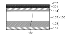
- Figure 3A shows the step of forming the semiconductor laminated structure 100, the first insulating layer 201 and the second insulating layer 202.
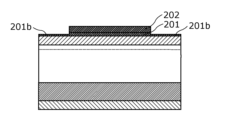
- Figure 3B shows the step of forming the thin portion 201b in the first insulating layer 201.
- Figure 3C shows the step of forming the through recess portion 211.
- Figure 3D shows the step of forming the contact layer 212.
- Figure 3E shows the step of forming the source electrode 301 and the drain electrode 302.
- Figure 3F shows the step of performing heat treatment.
- Figure 3G shows the step of forming the gate electrode 303.
- a semiconductor laminated structure 100 consisting of a buffer layer 102, an electron transit layer 103, and an electron supply layer 104 is formed on a substrate 101 using metal organic chemical vapor deposition (MOCVD) (semiconductor laminated structure formation process).
- MOCVD metal organic chemical vapor deposition
- a semiconductor laminated structure 100 is formed by epitaxially growing, in sequence, in the +c-plane direction ( ⁇ 0001> direction) on a substrate 101 made of Si, a buffer layer 102 made of a laminated structure of AlN and AlGaN with a layer thickness of 2 ⁇ m, an electron transit layer 103 made of GaN with a layer thickness of 200 nm, and an electron supply layer 104 made of AlGaN with a layer thickness of 20 nm and an Al composition ratio of 25%.
- a first insulating layer 201 is formed on the semiconductor laminated structure 100 as an insulating layer containing Si (first insulating layer forming process). Specifically, after forming the semiconductor laminated structure 100, the first insulating layer 201 made of SiN and having a layer thickness of 2 nm is formed in the same semiconductor crystal growth apparatus (MOCVD furnace). In other words, the first insulating layer 201 is formed on the electron supply layer 104 without exposure to the atmosphere. In this way, by forming the first insulating layer 201 directly on the electron supply layer 104 without exposure to the atmosphere, oxygen is not unevenly distributed between the electron supply layer 104 and the first insulating layer 201.
- MOCVD furnace semiconductor crystal growth apparatus
- the second insulating layer 202 is formed on the first insulating layer 201 (second insulating layer forming step). Specifically, after forming the first insulating layer 201, the semiconductor stacked structure 100 and the substrate 101 on which the first insulating layer 201 is formed are transferred to another device, and the second insulating layer 202 made of SiO2 and having a thickness of 50 nm is formed. In this structure, a high concentration of two-dimensional electron gas is generated on the electron transit layer 103 side of the heterointerface between the electron supply layer 104 and the electron transit layer 103, and a two-dimensional electron gas layer 105 is formed.
- the film formation conditions for forming the first insulating layer 201 and the second insulating layer 202 are, for example, a growth temperature of 900 to 1150° C. and source gases of SiH 4 and NH 3.
- a growth temperature 900 to 1150° C.
- source gases of SiH 4 and NH 3 SiH 4 and NH 3.
- a portion of the first insulating layer 201 is thinned to form a thin portion 201b in the first insulating layer 201 (thin portion forming process).
- a resist is applied onto the second insulating layer 202, and then the resist is patterned by lithography to form a mask (resist mask) on the second insulating layer 202 except for the regions where the contact layer 212, the electron supply assist layer 401, and the alloy layer 402 are to be formed.
- a mask resist mask
- openings are formed in the resist in the regions where the contact layer 212, the electron supply assist layer 401, and the alloy layer 402 are to be formed.
- openings are formed in the regions including the regions where the source side contact layer 212A and the drain side contact layer 212B are to be formed.
- etching is performed using the resist having the opening as a mask to remove a part of the second insulating layer 202 and thin a part of the first insulating layer 201.
- dry etching and wet etching are performed using the resist having the opening as a mask to selectively remove the second insulating layer 202 from the first insulating layer 201. That is, by performing dry etching and wet etching, the second insulating layer 202 is removed and the first insulating layer 201 is thinned in the region where the contact layer 212, the electron supply auxiliary layer 401, and the alloy layer 402 are formed. As a result, as shown in FIG.
- a part of the first insulating layer 201 (the region where the contact layer 212, the electron supply auxiliary layer 401, and the alloy layer 402 are formed) is thinned, and a thin portion 201b can be formed in the first insulating layer 201 as a remaining film.
- the mask (resist) and the polymer generated by the dry etching are removed.
- the second insulating layer 202 can be selectively removed with respect to the first insulating layer 201 by using DHF or BHF.
- the surface of the first insulating layer 201 may be oxidized to selectively remove only a portion of the first insulating layer 201.
- the thickness of the thin portion 201b (residual film) of the first insulating layer 201 is 2 nm or less. In this case, it is preferable that the thickness of the thin portion 201b (residual film) of the first insulating layer 201 is more than half the thickness of the first insulating layer 201 before thinning (i.e., more than half should be left), but this is not limited to this. As an example, if the thickness of the first insulating layer 201 before thinning is 2 nm, the thin portion 201b (residual film) of the first insulating layer 201 is 1.5 nm.
- a through recess 211 is formed that penetrates the thin portion 201b of the first insulating layer 201 and the electron supply layer 104 to reach the electron transit layer 103 while leaving a part of the thin portion 201b of the first insulating layer 201 as the insulating layer remaining portion 201b1.
- a resist is applied onto the second insulating layer 202 and onto a part of the thin portion 201b of the first insulating layer 201, and then the resist is patterned by lithography to form a mask (resist mask) in areas other than the area where the through recess portion 211 is to be formed.
- the resist forms an opening in the area where the through recess portion 211 is to be formed.
- the resist has an opening in each of the areas where the source side contact layer 212A and the drain side contact layer 212B are to be formed.
- dry etching is performed using the resist having the opening as a mask, thereby forming a through recess 211 that penetrates the end of the thin portion 201b of the first insulating layer 201 and the electron supply layer 104 to reach the electron transit layer 103 while leaving a part of the thin portion 201b of the first insulating layer 201 as the insulating layer remaining portion 201b1.
- two through recesses 211 are formed corresponding to the regions where the source side contact layer 212A and the drain side contact layer 212B are formed.
- the mask (resist) and the polymer generated by the dry etching are removed.
- the through recess portion 211 is formed by dry etching, but this is not limiting. Specifically, the through recess portion 211 may be formed by wet etching.
- the side of the electron supply layer 104 may be selectively wet etched using SPM, APM or KOH. This allows the side of the through recess 211 to be an inclined surface. Specifically, the side of the through recess 211 can be an inclined surface that includes an elevation angle of 5 degrees or less in the direction from the center of the bottom surface of the through recess 211 to the side.
- the contact layer 212 is embedded in the through recess portion 211 (contact layer formation process).
- n + -GaN is grown by MOCVD using the second insulating layer 202 and the insulating layer remaining portion 201b1 of the first insulating layer 201 as a mask so as to fill the two through-recess portions 211.
- the contact layer 212 filled in one of the two through-recess portions 211 is the source-side contact layer 212A, and the contact layer 212 filled in the other of the two through-recess portions 211 is the drain-side contact layer 212B.
- the contact layer 212 is formed by doping with Si as an n-type impurity and growing n + -GaN to a thickness of 100 nm.
- the Si doping concentration of the contact layer 212 is, for example, 2 ⁇ 10 19 /cm 3.
- the contact layer 212 may be formed by sputtering without being limited to regrowth, or may be formed by ion implantation, plasma treatment, or the like without forming the penetrating recess portion 211.
- the source electrode 301 and the drain electrode 302 are formed across the insulating layer remaining portion 201b1 of the first insulating layer 201 and the contact layer 212 (source electrode/drain electrode formation process).
- a 30 nm thick Ti film and a 200 nm thick Al film are deposited in this order by vapor deposition or sputtering to form a laminated film, and then unnecessary laminated film is removed by lift-off to form a source electrode 301 and a drain electrode 302 of a predetermined shape made of a laminated film of a Ti film and an Al film on the contact layer 212.
- the source electrode 301 is formed on the source side contact layer 212A
- the drain electrode 302 is formed on the drain side contact layer 212B. The resist mask and the polymer are then removed.
- the source electrode 301 and the drain electrode 302 are formed by deposition and lift-off, but this is not limited to the above.
- a Ti film and an Al film may be deposited in this order by sputtering to form a laminated film, and then the laminated film may be patterned using lithography and dry etching to form the source electrode 301 and the drain electrode 302 in a predetermined shape.
- a heat treatment is performed to form an electron supply auxiliary layer 401 and an alloy layer 402 in the insulating layer remaining portion 201b1 of the first insulating layer 201 and the electron supply layer 104 (heat treatment process).
- the temperature of this heat treatment is, for example, 400 to 600° C., and preferably 500 to 550° C.
- the heat treatment is preferably performed in an atmosphere that does not contain oxygen. In this embodiment, the heat treatment is performed at a temperature of 540° C. in an N2 atmosphere.
- the elements constituting the insulating layer remaining portion 201b1 of the first insulating layer 201 and the electron supply layer 104 and the elements constituting the source electrode 301 and the drain electrode 302 are mutually diffused and alloyed by the heat, forming the electron supply auxiliary layer 401 and the alloy layer 402.
- the first insulating layer 201 is an insulating layer containing Si
- the electron supply layer 104 is an AlGaN layer, so that the upper layer portion of the electron supply layer 104 in contact with the insulating layer remaining portion 201b1 of the first insulating layer 201 becomes n-type due to the formation of nitrogen vacancies caused by the diffusion of Si constituting the first insulating layer 201, and an n-type AlGaN layer is formed as the electron supply assistance layer 401.
- the electron supply assistance layer 401 which is an n-type semiconductor layer, is formed.
- the source electrode 301 and the drain electrode 302 contain Ti, the formation of nitrogen vacancies due to the diffusion of this Ti also causes the upper portion of the electron supply layer 104 to become n-type.
- the diffusion of Si and Ti due to heat treatment causes the upper portion of the electron supply layer 104 to become n-type, forming the electron supply auxiliary layer 401, which is an n-type semiconductor layer.
- the upper portion of the electron supply layer 104 becomes n-type to form the electron supply auxiliary layer 401, which is an n-type semiconductor layer, and a second two-dimensional electron gas layer 105B having a higher electron concentration than the first two-dimensional electron gas layer 105A is generated.
- the second two-dimensional electron gas layer 105B is electrically connected to the source electrode 301 and the drain electrode 302 in an ohmic connection.
- the insulating layer remaining portion 201b1 which is a part of the thin portion 201b of the first insulating layer 201, is thin.
- the thickness of the thin portion 201b of the first insulating layer 201 is 2 nm or less. In this way, it is possible to increase the Si content in the upper portion of the electron supply layer 104, and to make the upper portion of the electron supply layer 104 more n-type.
- the first insulating layer 201 is removed from the portion of the first insulating layer 201 that is spaced apart from the source electrode 301 and the drain electrode 302 to form the gate electrode 303 (gate electrode formation process).
- the second insulating layer 202 is formed on the first insulating layer 201, the first insulating layer 201 and the second insulating layer 202 are removed from the portion of the first insulating layer 201 and the second insulating layer 202 that is spaced apart from the source electrode 301 and the drain electrode 302 to form the gate electrode 303.
- a mask (resist mask) is formed by lithography except for the area where the gate electrode 303 is to be formed (the area where the gate electrode is to be formed).
- the second insulating layer 202 and the first insulating layer 201 are selectively removed by dry etching to form an opening 201a in the first insulating layer 201 so that the electron supply layer 104 is exposed, and an opening 202a in the second insulating layer 202 is formed.
- the mask (resist mask) and polymer generated by dry etching are removed.
- the gate electrode 303 is formed in the openings 201a and 202a.
- a laminated film is formed by depositing a TiN film having a layer thickness of 50 nm and an Al film having a layer thickness of 450 nm in this order by sputtering, and then the laminated film is patterned by lithography and dry etching to form the gate electrode 303 having a predetermined shape as shown in FIG. 3F. Then, the mask and polymer generated by dry etching are removed.
- Fig. 4 is a cross-sectional view showing the configuration of the semiconductor device 2 according to the second embodiment. Note that the following description will focus on the differences from the first embodiment, and the description of the commonalities will be omitted or simplified.
- the semiconductor device 2 according to this embodiment differs from the semiconductor device 1 according to the above-mentioned embodiment 1 in the configuration of the source electrode 301A and the drain electrode 302A.
- the source electrode 301A and the drain electrode 302A in this embodiment are the same as the source electrode 301 and the drain electrode 302 in the semiconductor device 1 according to the above-mentioned embodiment 1, and are integrated with the contact layer 212, which are made of the same material.
- the source electrode 301A in this embodiment is the same as the source electrode 301 and the source side contact layer 212A in the first embodiment, which are made of the same material and integrated together.
- the drain electrode 302A in this embodiment is the same as the drain electrode 302 and the drain side contact layer 212B in the first embodiment, which are made of the same material and integrated together.
- the semiconductor device 2 according to this embodiment does not have a contact layer made of a semiconductor material.
- the source electrode 301A and the drain electrode 302A are provided so as to fill the through recess portion 211.
- the source electrode 301A and the drain electrode 302A are provided so as to cover the alloy layer 402 and a part of the second insulating layer 202.
- the source electrode 301A and the drain electrode 302A are formed of a multilayer electrode film having a laminated structure in which, for example, a Ti film having a thickness of 30 nm and an Al film having a thickness of 200 nm are laminated in this order, but this is not limited to this.
- the source electrode 301A and the drain electrode 302A do not contain Au, but this is not limited to this.
- the material forming the source electrode 301A and the drain electrode 302A may be formed using Ti, Ta, Al, Hf, Ru, and Cu.
- the source electrode 301A and drain electrode 302A configured in this manner are electrically ohmically connected to the second two-dimensional electron gas layer 105B.
- the semiconductor device 2 according to this embodiment can also achieve the same effects as those of the above-mentioned embodiment 1.
- the present embodiment also includes the electron supply auxiliary layer 401, which is an n-type semiconductor layer, and the alloy layer 402, so that the electron concentration of the second two-dimensional electron gas layer 105B is greater than the electron concentration of the first two-dimensional electron gas layer 105A. This can reduce the decrease in the electron concentration in the portion adjacent to the side of the through recess portion 211 in the electron supply layer 104, and therefore can suppress a decrease in the maximum drain current.
- the source electrode 301A and the drain electrode 302A also function as contact layers, and no contact layer made of a semiconductor material is provided. This makes it possible to eliminate the process of forming the contact layer. Also, in the semiconductor device 2 according to this embodiment, the source electrode 301A and the drain electrode 302A do not contain Au, making it possible to reduce manufacturing costs.
- Figures 5A to 5F are cross-sectional views showing each step in the manufacturing method of the semiconductor device 2 according to the second embodiment.
- Figure 5A shows the step of forming the semiconductor laminated structure 100, the first insulating layer 201 and the second insulating layer 202.
- Figure 5B shows the step of forming the thin portion 201b in the first insulating layer 201.
- Figure 5C shows the step of forming the through recess portion 211.
- Figure 5D shows the step of forming the source electrode 301A and the drain electrode 302A.
- Figure 5E shows the step of performing heat treatment.
- Figure 5F shows the step of forming the gate electrode 303.
- a semiconductor laminated structure 100 consisting of a buffer layer 102, an electron transit layer 103, and an electron supply layer 104 is formed on a substrate 101 using MOCVD (semiconductor laminated structure formation process). This process is the same as the process in FIG. 3A in the first embodiment.
- MOCVD semiconductor laminated structure formation process
- a portion of the first insulating layer 201 is thinned to form a thin portion 201b in the first insulating layer 201 (thin portion forming process). This process is the same as the process in FIG. 3B in the first embodiment.
- a through recess 211 is formed that penetrates the thin portion 201b of the first insulating layer 201 and the electron supply layer 104 to reach the electron transit layer 103 while leaving a part of the thin portion 201b of the first insulating layer 201 as the insulating layer remaining portion 201b1.
- This process is the same as the process of FIG. 3C in the first embodiment.
- the source electrode 301A and the drain electrode 302A are embedded in the through recess 211 (source electrode/drain electrode formation process). Specifically, the source electrode 301A and the drain electrode 302A are formed across the insulating layer remnant 201b1 of the first insulating layer 201 and the through recess 211.
- the second insulating layer 202 and the first insulating layer 201 are used as masks to deposit a Ti film and an Al film in order by sputtering so as to fill the through recess 211 to form a laminated film, and then a mask is formed by lithography in the region where the source electrode 301A and the drain electrode 302A are to be formed.
- the region where this mask is formed is a region that straddles the through recess 211, the insulating layer remaining portion 201b1 of the first insulating layer 201, and the second insulating layer 202 in a plan view.
- the Al film and the Ti film other than the region where the mask is formed are removed by dry etching, so that the source electrode 301A and the drain electrode 302A are formed straddling the insulating layer remaining portion 201b1 of the first insulating layer 201 and the through recess 211. Then, the mask and the polymer are removed.
- a heat treatment is performed to form an electron supply auxiliary layer 401 and an alloy layer 402 in the insulating layer remaining portion 201b1 of the first insulating layer 201 and the electron supply layer 104 (heat treatment process).
- This process is the same as the process in FIG. 3F in the above-mentioned embodiment 1.
- the elements constituting the insulating layer remaining portion 201b1 of the first insulating layer 201 and the electron supply layer 104 and the elements constituting the source electrode 301A and the drain electrode 302A are mutually diffused and alloyed by heat, and the electron supply auxiliary layer 401 and the alloy layer 402 are formed.
- the first insulating layer 201 is removed from the portion of the first insulating layer 201 that is spaced apart from the source electrode 301A and the drain electrode 302A to form the gate electrode 303 (gate electrode formation process).
- the second insulating layer 202 is also formed on the first insulating layer 201, so the first insulating layer 201 and the second insulating layer 202 are removed from the portion of the first insulating layer 201 that is spaced apart from the source electrode 301A and the drain electrode 302A to form the gate electrode 303.
- This process is the same as the process of FIG. 3G in the first embodiment.
- the electron transit layer 103 and the electron supply layer 104 are made of a group III nitride semiconductor, but this is not limited thereto.
- the electron transit layer 103 and the electron supply layer 104 may be made of other semiconductor materials, such as a group III arsenide semiconductor.
- this disclosure also includes forms obtained by applying various modifications to the above embodiments that a person skilled in the art may conceive, and forms realized by arbitrarily combining the components and functions of the embodiments within the scope of the present disclosure.
- this disclosure also includes any combination of two or more claims from among the multiple claims described in the claims at the time of filing this application, within the scope of technical compatibility. For example, when a cited-form claim described in the claims at the time of filing this application is made into a multi-claim or multi-multi-claim so as to cite all of the higher claims within the scope of technical compatibility, the combination of all claims included in that multi-claim or multi-multi-claim is also included in this disclosure.
- the technology disclosed herein can be used in semiconductor devices such as switching transistors used in communication equipment and inverters that require high-speed operation, as well as in power supply circuits. Among these, the technology disclosed herein is particularly useful for high-frequency power devices that have a significant impact on heat generation due to ohmic contact resistance.
- Electron supply layer 105 Two-dimensional electron gas layer 105A First two-dimensional electron gas layer 105B Second two-dimensional electron gas layer 201 First insulating layer 201a Opening 201b Thin portion 201b1 Remaining insulating layer 202 Second insulating layer 202a Opening 211 Penetrating recess 212 Contact layer 212A Source side contact layer 212B Drain side contact layer 301, 301A Source electrode 302, 302A Drain electrode 303 Gate electrode 401 Electron supply auxiliary layer 402 Alloy layer
Landscapes
- Junction Field-Effect Transistors (AREA)
- Insulated Gate Type Field-Effect Transistor (AREA)
Priority Applications (3)
| Application Number | Priority Date | Filing Date | Title |
|---|---|---|---|
| CN202480021888.9A CN120898539A (zh) | 2023-03-30 | 2024-03-28 | 半导体装置及半导体装置的制造方法 |
| JP2024563414A JP7636644B1 (ja) | 2023-03-30 | 2024-03-28 | 半導体装置および半導体装置の製造方法 |
| US19/333,056 US20260020300A1 (en) | 2023-03-30 | 2025-09-18 | Semiconductor device and method for manufacturing semiconductor device |
Applications Claiming Priority (2)
| Application Number | Priority Date | Filing Date | Title |
|---|---|---|---|
| US202363493030P | 2023-03-30 | 2023-03-30 | |
| US63/493,030 | 2023-03-30 |
Related Child Applications (1)
| Application Number | Title | Priority Date | Filing Date |
|---|---|---|---|
| US19/333,056 Continuation US20260020300A1 (en) | 2023-03-30 | 2025-09-18 | Semiconductor device and method for manufacturing semiconductor device |
Publications (1)
| Publication Number | Publication Date |
|---|---|
| WO2024204537A1 true WO2024204537A1 (ja) | 2024-10-03 |
Family
ID=92906720
Family Applications (2)
| Application Number | Title | Priority Date | Filing Date |
|---|---|---|---|
| PCT/JP2024/012641 Ceased WO2024204537A1 (ja) | 2023-03-30 | 2024-03-28 | 半導体装置および半導体装置の製造方法 |
| PCT/JP2024/012638 Ceased WO2024204536A1 (ja) | 2023-03-30 | 2024-03-28 | 半導体装置および半導体装置の製造方法 |
Family Applications After (1)
| Application Number | Title | Priority Date | Filing Date |
|---|---|---|---|
| PCT/JP2024/012638 Ceased WO2024204536A1 (ja) | 2023-03-30 | 2024-03-28 | 半導体装置および半導体装置の製造方法 |
Country Status (5)
| Country | Link |
|---|---|
| US (2) | US20260020309A1 (https=) |
| JP (2) | JP7703809B2 (https=) |
| CN (2) | CN120898539A (https=) |
| TW (1) | TWI911695B (https=) |
| WO (2) | WO2024204537A1 (https=) |
Citations (6)
| Publication number | Priority date | Publication date | Assignee | Title |
|---|---|---|---|---|
| WO2015011870A1 (ja) * | 2013-07-25 | 2015-01-29 | パナソニックIpマネジメント株式会社 | 半導体装置 |
| JP2015090927A (ja) * | 2013-11-06 | 2015-05-11 | 富士通株式会社 | 化合物半導体装置及びその製造方法 |
| JP2017022214A (ja) * | 2015-07-08 | 2017-01-26 | 富士通株式会社 | 化合物半導体装置及びその製造方法 |
| JP2019012783A (ja) * | 2017-06-30 | 2019-01-24 | 富士通株式会社 | 化合物半導体装置及びその製造方法 |
| JP2019096774A (ja) * | 2017-11-24 | 2019-06-20 | 住友電気工業株式会社 | 窒化物半導体素子の製造方法 |
| JP2020013964A (ja) * | 2018-07-20 | 2020-01-23 | 住友電気工業株式会社 | 半導体装置の製造方法 |
Family Cites Families (19)
| Publication number | Priority date | Publication date | Assignee | Title |
|---|---|---|---|---|
| JP3727818B2 (ja) | 1999-03-19 | 2005-12-21 | 株式会社東芝 | 半導体装置の配線構造及びその形成方法 |
| US7901994B2 (en) * | 2004-01-16 | 2011-03-08 | Cree, Inc. | Methods of manufacturing group III nitride semiconductor devices with silicon nitride layers |
| JP4832722B2 (ja) * | 2004-03-24 | 2011-12-07 | 日本碍子株式会社 | 半導体積層構造およびトランジスタ素子 |
| JP2007048866A (ja) | 2005-08-09 | 2007-02-22 | Toshiba Corp | 窒化物半導体素子 |
| JP2008211172A (ja) * | 2007-01-31 | 2008-09-11 | Matsushita Electric Ind Co Ltd | 半導体装置および半導体装置の製造方法 |
| JP2008244454A (ja) * | 2007-02-26 | 2008-10-09 | Toshiba Corp | 半導体レーザ装置 |
| JP5347228B2 (ja) | 2007-03-05 | 2013-11-20 | 日本電気株式会社 | 電界効果トランジスタ |
| JP2009111204A (ja) * | 2007-10-31 | 2009-05-21 | Panasonic Corp | 電界効果トランジスタ及びその製造方法 |
| JP2010098076A (ja) | 2008-10-15 | 2010-04-30 | Sumitomo Electric Device Innovations Inc | 半導体装置の製造方法 |
| JP5737948B2 (ja) * | 2008-12-26 | 2015-06-17 | ルネサスエレクトロニクス株式会社 | ヘテロ接合電界効果トランジスタ、ヘテロ接合電界トランジスタの製造方法、および電子装置 |
| JP2013055224A (ja) * | 2011-09-05 | 2013-03-21 | Mitsubishi Electric Corp | 半導体装置およびその製造方法 |
| JP2014029991A (ja) * | 2012-06-29 | 2014-02-13 | Sharp Corp | 窒化物半導体装置の電極構造および窒化物半導体電界効果トランジスタ |
| JP6194769B2 (ja) * | 2013-11-12 | 2017-09-13 | 富士通株式会社 | 半導体装置及び半導体装置の製造方法 |
| JP2015226022A (ja) | 2014-05-29 | 2015-12-14 | キヤノン株式会社 | 半導体装置の製造方法 |
| JP6023825B2 (ja) * | 2015-01-14 | 2016-11-09 | 株式会社豊田中央研究所 | 半導体装置 |
| JP6642883B2 (ja) * | 2015-10-08 | 2020-02-12 | ローム株式会社 | 窒化物半導体装置およびその製造方法 |
| JP7099255B2 (ja) * | 2018-11-01 | 2022-07-12 | 富士通株式会社 | 化合物半導体装置、高周波増幅器及び電源装置 |
| WO2021246227A1 (ja) * | 2020-06-01 | 2021-12-09 | ヌヴォトンテクノロジージャパン株式会社 | 半導体装置および半導体装置の製造方法 |
| WO2023276972A1 (ja) * | 2021-07-01 | 2023-01-05 | ローム株式会社 | 窒化物半導体装置 |
-
2024
- 2024-03-28 JP JP2025511144A patent/JP7703809B2/ja active Active
- 2024-03-28 CN CN202480021888.9A patent/CN120898539A/zh active Pending
- 2024-03-28 TW TW113111607A patent/TWI911695B/zh active
- 2024-03-28 CN CN202480022422.0A patent/CN121014277A/zh active Pending
- 2024-03-28 JP JP2024563414A patent/JP7636644B1/ja active Active
- 2024-03-28 WO PCT/JP2024/012641 patent/WO2024204537A1/ja not_active Ceased
- 2024-03-28 WO PCT/JP2024/012638 patent/WO2024204536A1/ja not_active Ceased
-
2025
- 2025-09-18 US US19/333,037 patent/US20260020309A1/en active Pending
- 2025-09-18 US US19/333,056 patent/US20260020300A1/en active Pending
Patent Citations (6)
| Publication number | Priority date | Publication date | Assignee | Title |
|---|---|---|---|---|
| WO2015011870A1 (ja) * | 2013-07-25 | 2015-01-29 | パナソニックIpマネジメント株式会社 | 半導体装置 |
| JP2015090927A (ja) * | 2013-11-06 | 2015-05-11 | 富士通株式会社 | 化合物半導体装置及びその製造方法 |
| JP2017022214A (ja) * | 2015-07-08 | 2017-01-26 | 富士通株式会社 | 化合物半導体装置及びその製造方法 |
| JP2019012783A (ja) * | 2017-06-30 | 2019-01-24 | 富士通株式会社 | 化合物半導体装置及びその製造方法 |
| JP2019096774A (ja) * | 2017-11-24 | 2019-06-20 | 住友電気工業株式会社 | 窒化物半導体素子の製造方法 |
| JP2020013964A (ja) * | 2018-07-20 | 2020-01-23 | 住友電気工業株式会社 | 半導体装置の製造方法 |
Also Published As
| Publication number | Publication date |
|---|---|
| JP7703809B2 (ja) | 2025-07-07 |
| US20260020309A1 (en) | 2026-01-15 |
| WO2024204536A1 (ja) | 2024-10-03 |
| TWI911695B (zh) | 2026-01-11 |
| US20260020300A1 (en) | 2026-01-15 |
| TW202443918A (zh) | 2024-11-01 |
| JPWO2024204537A1 (https=) | 2024-10-03 |
| CN121014277A (zh) | 2025-11-25 |
| JP7636644B1 (ja) | 2025-02-26 |
| CN120898539A (zh) | 2025-11-04 |
| TW202505778A (zh) | 2025-02-01 |
| JPWO2024204536A1 (https=) | 2024-10-03 |
Similar Documents
| Publication | Publication Date | Title |
|---|---|---|
| US8907349B2 (en) | Semiconductor device and method of manufacturing the same | |
| JP4022708B2 (ja) | 半導体装置 | |
| JP4530171B2 (ja) | 半導体装置 | |
| JP3733420B2 (ja) | 窒化物半導体材料を用いたヘテロ接合電界効果型トランジスタ | |
| US20110133206A1 (en) | Compound semiconductor device | |
| US20070278507A1 (en) | Field effect transistor and method for fabricating the same | |
| CN101027780A (zh) | Ⅲ-v族高电子迁移率晶体管器件 | |
| JP2010206020A (ja) | 半導体装置 | |
| JP2010171416A (ja) | 半導体装置、半導体装置の製造方法および半導体装置のリーク電流低減方法 | |
| JP4474292B2 (ja) | 半導体装置 | |
| JP2011054809A (ja) | 窒化物半導体装置およびその製造方法 | |
| JP2015106627A (ja) | 半導体積層基板 | |
| JP5304134B2 (ja) | 窒化物半導体装置およびその製造方法 | |
| JP6166508B2 (ja) | 半導体装置及び半導体装置の製造方法 | |
| JP4517077B2 (ja) | 窒化物半導体材料を用いたヘテロ接合電界効果型トランジスタ | |
| JP7636644B1 (ja) | 半導体装置および半導体装置の製造方法 | |
| JP7231826B2 (ja) | 半導体装置、半導体装置の製造方法及び電子装置 | |
| US6933181B2 (en) | Method for fabricating semiconductor device | |
| TWI921769B (zh) | 半導體裝置及半導體裝置的製造方法 | |
| JP2006286698A (ja) | 電子デバイス及び電力変換装置 | |
| CN117954319A (zh) | 电流孔垂直式电子晶体管及形成其的制造方法 | |
| CN223246958U (zh) | 一种半导体器件 | |
| JP4268099B2 (ja) | 窒化物系化合物半導体装置及びその製造方法 | |
| JP4546051B2 (ja) | 半導体装置の製造方法 | |
| US20250006798A1 (en) | Nitride semiconductor device and manufacturing method therefor |
Legal Events
| Date | Code | Title | Description |
|---|---|---|---|
| WWE | Wipo information: entry into national phase |
Ref document number: 2024563414 Country of ref document: JP |
|
| 121 | Ep: the epo has been informed by wipo that ep was designated in this application |
Ref document number: 24780637 Country of ref document: EP Kind code of ref document: A1 |
|
| WWE | Wipo information: entry into national phase |
Ref document number: 202480021888.9 Country of ref document: CN |
|
| NENP | Non-entry into the national phase |
Ref country code: DE |
|
| WWP | Wipo information: published in national office |
Ref document number: 202480021888.9 Country of ref document: CN |
|
| 122 | Ep: pct application non-entry in european phase |
Ref document number: 24780637 Country of ref document: EP Kind code of ref document: A1 |