WO2024157366A1 - はんだ合金、接合部、接合材、ソルダペースト、接合構造体および電子制御装置 - Google Patents
はんだ合金、接合部、接合材、ソルダペースト、接合構造体および電子制御装置 Download PDFInfo
- Publication number
- WO2024157366A1 WO2024157366A1 PCT/JP2023/002160 JP2023002160W WO2024157366A1 WO 2024157366 A1 WO2024157366 A1 WO 2024157366A1 JP 2023002160 W JP2023002160 W JP 2023002160W WO 2024157366 A1 WO2024157366 A1 WO 2024157366A1
- Authority
- WO
- WIPO (PCT)
- Prior art keywords
- mass
- joint
- solder alloy
- solder
- joined
- Prior art date
- Legal status (The legal status is an assumption and is not a legal conclusion. Google has not performed a legal analysis and makes no representation as to the accuracy of the status listed.)
- Ceased
Links
Images
Classifications
-
- B—PERFORMING OPERATIONS; TRANSPORTING
- B23—MACHINE TOOLS; METAL-WORKING NOT OTHERWISE PROVIDED FOR
- B23K—SOLDERING OR UNSOLDERING; WELDING; CLADDING OR PLATING BY SOLDERING OR WELDING; CUTTING BY APPLYING HEAT LOCALLY, e.g. FLAME CUTTING; WORKING BY LASER BEAM
- B23K35/00—Rods, electrodes, materials, or media, for use in soldering, welding, or cutting
- B23K35/02—Rods, electrodes, materials, or media, for use in soldering, welding, or cutting characterised by mechanical features, e.g. shape
- B23K35/0222—Rods, electrodes, materials, or media, for use in soldering, welding, or cutting characterised by mechanical features, e.g. shape for use in soldering or brazing
- B23K35/0244—Powders, particles or spheres; Preforms made therefrom
-
- B—PERFORMING OPERATIONS; TRANSPORTING
- B23—MACHINE TOOLS; METAL-WORKING NOT OTHERWISE PROVIDED FOR
- B23K—SOLDERING OR UNSOLDERING; WELDING; CLADDING OR PLATING BY SOLDERING OR WELDING; CUTTING BY APPLYING HEAT LOCALLY, e.g. FLAME CUTTING; WORKING BY LASER BEAM
- B23K35/00—Rods, electrodes, materials, or media, for use in soldering, welding, or cutting
- B23K35/22—Rods, electrodes, materials, or media, for use in soldering, welding, or cutting characterised by the composition or nature of the material
- B23K35/24—Selection of soldering or welding materials proper
- B23K35/26—Selection of soldering or welding materials proper with the principal constituent melting at less than 400°C
- B23K35/262—Sn as the principal constituent
-
- B—PERFORMING OPERATIONS; TRANSPORTING
- B23—MACHINE TOOLS; METAL-WORKING NOT OTHERWISE PROVIDED FOR
- B23K—SOLDERING OR UNSOLDERING; WELDING; CLADDING OR PLATING BY SOLDERING OR WELDING; CUTTING BY APPLYING HEAT LOCALLY, e.g. FLAME CUTTING; WORKING BY LASER BEAM
- B23K35/00—Rods, electrodes, materials, or media, for use in soldering, welding, or cutting
- B23K35/02—Rods, electrodes, materials, or media, for use in soldering, welding, or cutting characterised by mechanical features, e.g. shape
- B23K35/0222—Rods, electrodes, materials, or media, for use in soldering, welding, or cutting characterised by mechanical features, e.g. shape for use in soldering or brazing
- B23K35/0244—Powders, particles or spheres; Preforms made therefrom
- B23K35/025—Pastes, creams or slurries
-
- B—PERFORMING OPERATIONS; TRANSPORTING
- B23—MACHINE TOOLS; METAL-WORKING NOT OTHERWISE PROVIDED FOR
- B23K—SOLDERING OR UNSOLDERING; WELDING; CLADDING OR PLATING BY SOLDERING OR WELDING; CUTTING BY APPLYING HEAT LOCALLY, e.g. FLAME CUTTING; WORKING BY LASER BEAM
- B23K35/00—Rods, electrodes, materials, or media, for use in soldering, welding, or cutting
- B23K35/22—Rods, electrodes, materials, or media, for use in soldering, welding, or cutting characterised by the composition or nature of the material
- B23K35/24—Selection of soldering or welding materials proper
- B23K35/26—Selection of soldering or welding materials proper with the principal constituent melting at less than 400°C
-
- B—PERFORMING OPERATIONS; TRANSPORTING
- B23—MACHINE TOOLS; METAL-WORKING NOT OTHERWISE PROVIDED FOR
- B23K—SOLDERING OR UNSOLDERING; WELDING; CLADDING OR PLATING BY SOLDERING OR WELDING; CUTTING BY APPLYING HEAT LOCALLY, e.g. FLAME CUTTING; WORKING BY LASER BEAM
- B23K35/00—Rods, electrodes, materials, or media, for use in soldering, welding, or cutting
- B23K35/22—Rods, electrodes, materials, or media, for use in soldering, welding, or cutting characterised by the composition or nature of the material
- B23K35/24—Selection of soldering or welding materials proper
- B23K35/26—Selection of soldering or welding materials proper with the principal constituent melting at less than 400°C
- B23K35/264—Bi as the principal constituent
-
- B—PERFORMING OPERATIONS; TRANSPORTING
- B23—MACHINE TOOLS; METAL-WORKING NOT OTHERWISE PROVIDED FOR
- B23K—SOLDERING OR UNSOLDERING; WELDING; CLADDING OR PLATING BY SOLDERING OR WELDING; CUTTING BY APPLYING HEAT LOCALLY, e.g. FLAME CUTTING; WORKING BY LASER BEAM
- B23K35/00—Rods, electrodes, materials, or media, for use in soldering, welding, or cutting
- B23K35/22—Rods, electrodes, materials, or media, for use in soldering, welding, or cutting characterised by the composition or nature of the material
- B23K35/36—Selection of non-metallic compositions, e.g. coatings or fluxes; Selection of soldering or welding materials, conjoint with selection of non-metallic compositions, both selections being of interest
- B23K35/3601—Selection of non-metallic compositions, e.g. coatings or fluxes; Selection of soldering or welding materials, conjoint with selection of non-metallic compositions, both selections being of interest with inorganic compounds as principal constituents
-
- B—PERFORMING OPERATIONS; TRANSPORTING
- B23—MACHINE TOOLS; METAL-WORKING NOT OTHERWISE PROVIDED FOR
- B23K—SOLDERING OR UNSOLDERING; WELDING; CLADDING OR PLATING BY SOLDERING OR WELDING; CUTTING BY APPLYING HEAT LOCALLY, e.g. FLAME CUTTING; WORKING BY LASER BEAM
- B23K35/00—Rods, electrodes, materials, or media, for use in soldering, welding, or cutting
- B23K35/22—Rods, electrodes, materials, or media, for use in soldering, welding, or cutting characterised by the composition or nature of the material
- B23K35/36—Selection of non-metallic compositions, e.g. coatings or fluxes; Selection of soldering or welding materials, conjoint with selection of non-metallic compositions, both selections being of interest
- B23K35/3612—Selection of non-metallic compositions, e.g. coatings or fluxes; Selection of soldering or welding materials, conjoint with selection of non-metallic compositions, both selections being of interest with organic compounds as principal constituents
- B23K35/3613—Polymers, e.g. resins
-
- C—CHEMISTRY; METALLURGY
- C22—METALLURGY; FERROUS OR NON-FERROUS ALLOYS; TREATMENT OF ALLOYS OR NON-FERROUS METALS
- C22C—ALLOYS
- C22C12/00—Alloys based on antimony or bismuth
-
- C—CHEMISTRY; METALLURGY
- C22—METALLURGY; FERROUS OR NON-FERROUS ALLOYS; TREATMENT OF ALLOYS OR NON-FERROUS METALS
- C22C—ALLOYS
- C22C13/00—Alloys based on tin
- C22C13/02—Alloys based on tin with antimony or bismuth as the next major constituent
Definitions
- the present invention relates to a solder alloy, a joint, a joint material, a solder paste, a joint structure, and an electronic control device.
- the joining conditions between materials to be joined are set depending on the application of the electronic device and the material and heat resistance of the components that make up the electronic device.
- a solder alloy that melts at or below the set heating temperature is used as the joining material.
- a method for lowering the melting temperature of a solder alloy which means the "melting point” or “liquidus temperature” in this specification
- a method of adding Bi to the solder alloy has been proposed.
- Bi is hard and brittle, it reduces the ductility of the solder alloy.
- solder alloys for example, are provided as Bi-containing solder alloys with improved ductility.
- a SnBiSb-based low-temperature lead-free solder characterized in that the lead-free solder is composed of, by mass percentage, 32.8-56.5% Bi, 0.7-2.2% Sb, and the remainder Sn, and the mass percentages of Bi and Sb satisfy the relational expression b 0.006a2 - 0.672a + 19.61 + c, where a indicates the mass percentage of Bi and b indicates the mass percentage of Sb, and the value range of c is -1.85 ⁇ c ⁇ 1.85, and further contains, by mass percentage, one or more of the following metal elements: 0.01-2.5%, 0.05-2.0%, 0.5-0.8% Ag, and 0.05-1% In (Patent Document 3).
- the joint structure (herein, this refers to a structure in which multiple joined materials are joined via joints) inside the electronic device may be placed in an environment where heat cycles are repeated. This heat cycle can cause thermal fatigue failure (cracks) in the joints.
- Cracks thermal fatigue failure
- Bi reduces the ductility of the solder alloy, so the above-mentioned cracks are likely to occur in joints formed with a Bi-containing solder alloy.
- a method (through-hole mounting method) is used in which a through-hole is provided in a printed wiring board, the terminal of the electronic component is inserted into the through-hole, and the two are joined together, and the terminal of the electronic component in the through-hole and the land (electrode) of the printed wiring board are joined via a joint (fillet) formed on the printed wiring board.
- the molten solder hardens from the through-hole side toward the printed wiring board side during cooling, so that residual stress tends to concentrate on the land side of the formed bonded portion.
- the printed wiring board also thermally shrinks in the vertical direction. Therefore, in this case, the bonded portion is likely to peel off from the land (lift-off). This lift-off is particularly likely to occur when a solder alloy containing Bi is used for bonding.
- Patent Documents 1 to 3 do not disclose or suggest a solder alloy that has resistance to the above-mentioned cracks (hereinafter referred to in this specification as “heat cycle resistance”) and resistance to the above-mentioned external forces (hereinafter referred to in this specification as “drop impact resistance”) and that suppresses the occurrence of lift-off.
- heat cycle resistance resistance to the above-mentioned cracks
- drop impact resistance resistance to the above-mentioned external forces
- the object of the present invention is to solve the above problems by providing a solder alloy, a joining material, and a solder paste that contain Bi and can form a joint that has heat cycle resistance and drop impact resistance and suppresses the occurrence of lift-off.
- the solder alloy of the present invention contains 35% by mass or more and 65% by mass or less of Bi, 0.1% by mass or more and 0.65% by mass or less of Sb, 0.05% by mass or more and 2% by mass or less of Ag, and the remainder is Sn and unavoidable impurities.
- solder alloy of the present invention further contains one or more elements selected from the group consisting of P, Ga, and Ge in a total amount of 0.001% by mass or more and 0.05% by mass or less.
- the solder alloy of the present invention preferably further contains one or more elements selected from the group consisting of Mn, Ti, Al, Cr, V, Fe, Mg, Pd, Pb, and Mo in a total amount of 0.001% by mass or more and 0.05% by mass or less.
- the bonding material of the present invention contains a solder alloy described in any one of (1) to (3) above.
- the solder paste of the present invention contains a powder of the solder alloy described in any one of (1) to (3) above, and a flux containing a base resin, a thixotropic agent, an activator, and a solvent.
- the joint of the present invention is formed from a solder alloy described in any one of (1) to (3) above.
- the joint of the present invention is formed from the joint material described in (4) above.
- the joint of the present invention is formed from the solder paste described in (5) above.
- the joined structure of the present invention has a first joined material, a joining portion, and a second joined material, the joining portion being a joining portion described in any one of (6) to (8) above, and the first joined material and the second joined material being joined via the joining portion.
- the electronic control device of the present invention has the joint structure described in (9) above.
- solder alloy, bonding material, and solder paste of the present invention contain Bi, and can form a bond that has heat cycle resistance and drop impact resistance and can suppress the occurrence of lift-off.
- solder alloy of the present embodiment contains 35 mass % or more and 65 mass % or less of Bi, 0.1 mass % or more and 0.65 mass % or less of Sb, 0.05 mass % or more and 2 mass % or less of Ag, and the remainder is Sn and inevitable impurities.
- the solder alloy of this embodiment contains a predetermined amount of each of Bi, Sb, Ag, and Sn, which allows the solder alloy to have a well-balanced improvement in strength and ductility while still containing Bi.
- the solder alloy of this embodiment can suppress plastic deformation and slip deformation at the tip of the crack, and inhibit the progression of the crack, even if a crack occurs in the joint due to repeated heat cycles and stress is concentrated in the crack.
- the solder alloy of this embodiment can suppress damage to the joint caused by the action of a sudden and concentrated strong external force (hereinafter simply referred to as "external force") on the joint, such as when an electronic device is dropped.
- external force a sudden and concentrated strong external force
- a joint that is resistant to plastic deformation absorbs less of the impact energy generated by the action of the above-mentioned external force, and the impact energy that cannot be absorbed will damage the joint.
- the above-mentioned external force acts on the joint from multiple directions (at least two of tension, compression, shear, bending, and torsion).
- the solder alloy of this embodiment can form a joint having good balance between strength and ductility due to the above-mentioned configuration, and therefore can provide a joint having good resistance to the above-mentioned external force, that is, good drop impact resistance.
- the solder alloy of this embodiment can easily relieve the residual stress that occurs in the joint when the solder solidifies, and can suppress the occurrence of cracks in the joint caused by the residual stress and the occurrence of the lift-off described above.
- the solder alloy of the present embodiment contains 35% by mass to 65% by mass of Bi, which reduces the melting temperature of the solder alloy while suppressing a decrease in the ductility of the solder alloy, and also strengthens the joint through the solid solution of Bi in Sn, thereby improving the strength and ductility of the joint in a well-balanced manner.
- the preferred Bi content is 35 mass% or more and 60 mass% or less. Furthermore, the more preferred Bi content is 40 mass% or more and 59 mass% or less.
- the preferred Bi content can be 50 mass% or more, or 54 mass% or more, and can also be 58 mass% or less, 56.5 mass% or less, or 56 mass% or less. By keeping the Bi content within this range, the ductility and strength of the joint can be further improved.
- the solder alloy of the present embodiment contains 0.1 mass % or more and 0.65 mass % or less of Sb, which allows the joint to be solid-solution strengthened by the dissolution of Sb into Sn, and the strengthening and ductility of the joint to be improved by the precipitation and dispersion of fine ⁇ -SnSb intermetallic compounds, thereby enabling the strength and ductility of the joint to be improved in a well-balanced manner.
- the Sb content is less than 0.1 mass%, there is a risk that the joint will not be sufficiently strengthened. Also, if the Sb content exceeds 0.65 mass%, coarse ⁇ -SnSb intermetallic compounds will crystallize as primary crystals, which may impair the ductility of the joint.
- the preferred Sb content is 0.2 mass% or more and 0.65 mass% or less. Furthermore, the more preferred Sb content is 0.3 mass% or more and 0.65 mass% or less. By keeping the Sb content within this range, the ductility and strength of the joint can be further improved.
- the solder alloy of the present embodiment contains 0.05% by mass to 2% by mass of Ag, which lowers the melting temperature of the solder alloy and improves the strength and ductility of the joint by precipitation and dispersion of fine Ag 3 Sn intermetallic compounds, thereby improving the strength and ductility of the joint in a well-balanced manner.
- the precipitation strengthening of the joint may be insufficient, and if the Ag content exceeds 2 mass %, the Ag 3 Sn intermetallic compound may become coarse, which may impair the ductility of the joint.
- the preferred Ag content is 0.1% by mass or more and 1.5% by mass or less.
- the preferred Ag content can be 1% by mass or less, 0.8% by mass or less, or 0.5% by mass or less.
- the more preferred Ag content is 0.2% by mass or more and 0.4% by mass or less.
- the solder alloy of this embodiment may further contain at least one element selected from the group consisting of P, Ga, and Ge in a total amount of 0.001% by mass to 0.05% by mass.
- at least one element selected from the group consisting of P, Ga, and Ge By adding at least one element selected from the group consisting of P, Ga, and Ge to the solder alloy, oxidation of the solder alloy can be suppressed and the wettability of the solder alloy can be improved, making it possible to provide a highly reliable joint.
- the total content of one or more elements selected from the group consisting of P, Ga, and Ge exceeds 0.05 mass %, voids may occur in the joint, which may deteriorate the heat cycle resistance of the joint.
- the solder alloy of this embodiment may further contain one or more elements selected from the group consisting of Mn, Ti, Al, Cr, V, Fe, Mg, Pd, Pb, and Mo in a total amount of 0.001 mass % or more and 0.05 mass % or less.
- the total content of one or more selected from Mn, Ti, Al, Cr, V, Fe, Mg, Pd, Pb, and Mo exceeds 0.05 mass%, voids may be generated in the joint, and the heat cycle resistance may be deteriorated.
- Fe is added to the solder alloy of this embodiment, if the Fe content exceeds 0.05 mass %, there is a risk that needle-shaped substances are likely to be generated in the solder alloy during the manufacturing process of the solder alloy.
- the presence of these needle-shaped substances may hinder the powdering, making it difficult to powder into spherical shapes.
- solder alloy of this embodiment is made up of Sn and inevitable impurities.
- the solder alloy of this embodiment may contain alloy elements other than the alloy elements described above as inevitable impurities.
- the bonding material of the present embodiment contains the solder alloy of the present embodiment, and can be used in the form of a solder paste, a solder ball, a wire, a solder preform, a flux cored solder, etc., which will be described later.
- the form of the bonding material can be appropriately selected depending on the size, type, and application of the materials to be bonded, the solder bonding method, etc.
- the joining material of this embodiment can form a joining portion that has heat cycle resistance and drop impact resistance, while lowering the melting temperature by adding Bi, and suppresses the occurrence of lift-off.
- solder paste of the present embodiment contains the solder alloy of the present embodiment in powder form (hereinafter referred to as "alloy powder"), and is produced, for example, by kneading the alloy powder with a flux to form a paste.
- the flux may include, for example, a base resin, a thixotropic agent, an activator, and a solvent.
- the base resin may, for example, be a rosin-based resin; an acrylic resin obtained by polymerizing at least one monomer such as acrylic acid, methacrylic acid, various esters of acrylic acid, various esters of methacrylic acid, crotonic acid, itaconic acid, maleic acid, maleic anhydride, esters of maleic acid, esters of maleic anhydride, acrylonitrile, methacrylonitrile, acrylamide, methacrylamide, vinyl chloride, or vinyl acetate; an epoxy resin; or a phenolic resin. These may be used alone or in combination.
- an acrylic resin obtained by polymerizing at least one monomer such as acrylic acid, methacrylic acid, various esters of acrylic acid, various esters of methacrylic acid, crotonic acid, itaconic acid, maleic acid, maleic anhydride, esters of maleic acid, esters of maleic anhydride, acrylonitrile, methacrylonitrile, acrylamide, methacrylamide, vinyl
- thixotropic agent examples include hydrogenated castor oil, hydrogenated castor oil, bisamide-based thixotropic agents (saturated fatty acid bisamide, unsaturated fatty acid bisamide, aromatic bisamide, etc.), oxyfatty acids, dimethyldibenzylidenesorbitol, etc. These can be used alone or in combination.
- the activators include, for example, organic acids (monocarboxylic acids, dicarboxylic acids, other organic acids), halogen-containing compounds, amine-based activators, etc. These can be used alone or in combination.
- the solvent may be, for example, an alcohol-based solvent, a butyl cellosolve-based solvent, a glycol ether-based solvent, an ester-based solvent, or the like. These may be used alone or in combination.
- the flux may contain an antioxidant, such as a hindered phenol-based antioxidant, a phenol-based antioxidant, a bisphenol-based antioxidant, or a polymer-type antioxidant.
- the flux may further contain additives such as a matting agent and an antifoaming agent.
- the blending ratio (mass%) of the alloy powder to the flux can be 65:35 to 95:5 in terms of alloy powder:flux ratio.
- the blending ratio can be 85:15 to 93:7 or 87:13 to 92:8.
- the particle diameter of the alloy powder can be 1 ⁇ m or more and 40 ⁇ m or less.
- the particle diameter can also be 5 ⁇ m or more and 35 ⁇ m or less, or 10 ⁇ m or more and 30 ⁇ m or less.
- the particle diameter of the alloy powder can be changed as appropriate.
- the solder paste of this embodiment contains the alloy powder, and by adding Bi, the melting temperature can be lowered, while a joint that has heat cycle resistance and drop impact resistance and suppresses the occurrence of lift-off can be formed.
- the joint of the present embodiment is formed using the solder alloy and joint material (hereinafter, unless otherwise specified, including solder paste) of the present embodiment, and joins materials to be joined together.
- the method for forming the joint of this embodiment may be any method that can be formed using the solder alloy and the joint material of this embodiment, and any method such as a reflow method, a flow method, etc.
- the form of the joint material to be used may also be appropriately selected depending on the size, type, and use of the materials to be joined, the method for forming the joint, etc.
- the joined structure of the present embodiment includes a first joined material, a joining portion, and a second joined material.
- the joining portion is the joining portion of the present embodiment, and the first joined material and the second joined material are joined via the joining portion.
- the first and second bonded materials may be, for example, a substrate (a substrate whose surface is made of ceramic, metal, alloy, or resin and on which no electronic circuit is formed), a printed wiring board (a substrate on which an electronic circuit is formed and on which no electronic components or the like are mounted), a printed circuit board (a printed wiring board on which electronic components or the like are mounted), an electronic component, a silicon wafer, a semiconductor package, a semiconductor chip, etc. Bonded materials of different types may be combined, or bonded materials of the same type may be combined. Specific combinations include, for example, a printed wiring board and an electronic component, a printed wiring board and a semiconductor chip, a semiconductor package and a printed circuit board, and a printed wiring board and a printed wiring board.
- the joint structure of this embodiment is produced, for example, by the following method.
- the joining material of this embodiment is placed (or applied in the case of solder paste) at a predetermined position of the first material to be joined, for example, on an electronic circuit, and the second material to be joined is placed on the joining material.
- a predetermined heating temperature for example, a peak temperature of 200° C.
- solder preform when used as the joining material, a solder preform having a flux applied to its surface is placed at a predetermined position on the first joining material, and the second joining material is placed on the solder preform and heated.
- solder paste is applied to a surface of the BGA or to a predetermined position of the first material to be joined, and the second material to be joined is placed on the predetermined position of the first material to be joined and heated.
- the joint structure of this embodiment has the joint of this embodiment.
- the joint structure of this embodiment has heat cycle resistance and drop impact resistance, is less susceptible to lift-off, and can maintain high reliability.
- the electronic control device of the present embodiment includes the joint structure of the present embodiment, and is, for example, a printed circuit board in which an electronic component and a printed wiring board are joined, disposed in a housing, and controls the operation of components that constitute an electronic device.
- the electronic control device of the present embodiment includes the joining structure of the present embodiment, which allows the electronic control device of the present embodiment to have heat cycle resistance and drop impact resistance, and is also less susceptible to lift-off, thereby maintaining high reliability.
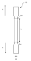
- test piece 10 was pulled in the X direction at room temperature with a stroke of 0.72 mm/min using a bench-top precision universal testing machine (product name: Autograph AG-50kNX plus, manufactured by Shimadzu Corporation) until it broke.
- the stroke distance when the test piece 10 broke was defined as GL1
- the length L of the central parallel part of the test piece before tension was defined as GL0.
- the elongation of the test piece 10 was calculated based on the following formula.
- Elongation rate (%) (GL1 - GL0) / GL0 x 100
- Five test pieces 10 were prepared for each type of solder alloy, and the elongation and the average value of the elongation were calculated for each according to the above procedure, and evaluated based on the following criteria. The results are shown in Tables 4 to 6.
- solder paste was prepared by kneading a flux containing the following components with a solder alloy powder (powder particle size 20 ⁇ m to 38 ⁇ m) shown in Tables 1 to 3 in the following mixing ratios (mass %).
- the solder alloy powder was prepared by atomization.
- Solder alloy powder: flux 89:11 ⁇ Flux composition> Hydrogenated acid modified rosin (product name: KE-604, manufactured by Arakawa Chemical Industries, Ltd.): 49% by mass Surfactant (glutaric acid: 0.3% by mass, suberic acid: 2% by mass, malonic acid: 0.5% by mass, dodecanedioic acid: 2% by mass, dibromobutenediol: 2% by mass) Fatty acid amide (product name: Slipax ZHH, manufactured by Nippon Kasei Co., Ltd.): 6% by mass Diethylene glycol monohexyl ether: 35.2% by mass Hindered phenol-based antioxidant (product name: Irganox 245, manufactured by BASF Japan Ltd.): 3% by mass
- the following tools were prepared: - LGA (Land Grid Array, pitch width: 0.5 mm, size: length 12 mm x width 12 mm x thickness 1 mm, number of terminals: 228 pins) Glass epoxy board (base material: FR-4, surface treatment: Cu-OSP, thickness: 1.0 mm, with a pattern capable of mounting the above LGA) - Metal mask (thickness: 100 ⁇ m, corresponding to the above pattern) For each solder paste, five of the glass epoxy substrates and 20 LGAs were used. Using the above tools and each solder paste, each test board was produced according to the following procedure, and a drop impact test was performed.
- LGA Linear Array, pitch width: 0.5 mm, size: length 12 mm x width 12 mm x thickness 1 mm, number of terminals: 228 pins
- Glass epoxy board base material: FR-4, surface treatment: Cu-OSP, thickness: 1.0 mm, with a pattern capable of mounting the above LGA
- - Metal mask
- solder paste was printed on the glass epoxy board using a metal mask.
- Four LGAs were placed on each glass epoxy board at the designated positions on the printed solder paste. The thickness of the printed solder paste was adjusted by the metal mask.
- the glass epoxy board on which the LGA was placed was then reflowed using a reflow furnace (product name: TNV-M6110CR, manufactured by Tamura Corporation) to produce a test board having an LGA, a glass epoxy board, and a joint for joining them.
- the preheat was 100° C. to 120° C.
- the peak temperature was 200° C.
- the time at or above 150° C. was 60 seconds
- the cooling rate from the peak temperature to 100° C. was 1° C. to 4° C./sec.
- the oxygen concentration was set to 200 ⁇ 100 ppm.
- the prepared test substrate was subjected to a drop impact test under the following conditions using a drop impact tester (product name: HDST-150J, Shin-Ei Technology Co., Ltd.). That is, in accordance with the JEDEC standard JESD22-B111, the test board was repeatedly dropped from a height where a shock waveform with an acceleration of 1,500 G and a width of 0.5 ms was applied. During the drop impact test, the electrical resistance of each joint of the test board was constantly observed, and when the resistance value exceeded 1,000 ⁇ , it was judged that the board had broken, and the number of drops until the board broke was counted.
- a drop impact tester product name: HDST-150J, Shin-Ei Technology Co., Ltd.
- the characteristic life is 110 times or more.
- the characteristic life is 90 times or more and less than 110 times.
- the characteristic life is 70 times or more and less than 90 times.
- the characteristic life is less than 70 times.
- solder paste was printed on the glass epoxy board using a metal mask. Then, 10 chip components were placed on each glass epoxy board at predetermined positions on the printed solder paste. The thickness of the printed solder paste was adjusted by the metal mask.
- the glass epoxy substrate on which the chip components were placed was then reflowed using a reflow furnace (product name: TNV-M6110CR, manufactured by Tamura Corporation) to produce three mounting substrates having chip components, glass epoxy substrates, and joints for joining them.
- the preheat was 100° C. to 120° C.
- the peak temperature was 200° C.
- the time at or above 150° C. was 60 seconds
- the cooling rate from the peak temperature to 100° C. was 1° C. to 4° C./sec.
- the oxygen concentration was set to 200 ⁇ 100 ppm.
- each mounting board was exposed to a thermal shock cycle as follows, with one cycle being set from -40°C (30 minutes) to 125°C (30 minutes), to produce test boards a to c.
- a target portion of each of the test substrates a to c was cut out and sealed with epoxy resin (product name: HERZOG epoxy low viscosity resin (base agent and hardener), manufactured by Herzog Japan Co., Ltd.). Then, a wet polishing machine (product name: TegraPol-25, manufactured by Marumoto Struers, Ltd.) was used to make the central cross section of each chip component mounted on each test board visible, and a scanning electron microscope (product name: TM-1000, manufactured by Hitachi High-Technologies Corporation) was used to observe the state of each joint on each of test boards a to c to check for the presence or absence of cracks that completely crossed the joints, and evaluation was performed according to the following criteria. The results are shown in Tables 4 to 6.
- Lift-off occurrence confirmation test The following tools were prepared. ⁇ Connector parts (product name: S15B-EH(LF)(SN), manufactured by JST Mfg. Co., Ltd.) Glass epoxy board (base material: FR-4, surface treatment: Cu-OSP, size: 50 mm x 50 mm, thickness: 1.6 mm, 2.5 mm pitch, with 1.6 diameter lands and 1.0 mm diameter through holes) A 200 ⁇ m thick metal mask having an opening pattern with a diameter of 3 mm and a pitch of 5 mm. Using the above tools and each solder paste, each test board was produced in the following manner and a lift-off occurrence confirmation test was performed.
- solder paste was printed on the glass epoxy board using a metal mask. Then, the terminals of the connector parts were inserted into the designated through-holes in the glass epoxy board, and reflow was performed using a reflow oven (product name: TNP-538EM, manufactured by Tamura Corporation) to create a test board with a solder joint (fillet) that joins the connector parts to the glass epoxy board. The reflow was performed under the same conditions as in (2) Drop Impact Test.
- solder alloy powder was prepared from each solder ingot under the following conditions. First, 50 g of a solder ingot, 890 g of castor oil, and 10 g of hydrogenated acid-modified rosin (product name: KE-604, manufactured by Arakawa Chemical Industries, Ltd.) were placed in a 2 L stainless steel beaker, and the mixture was continuously heated using a mantle heater.
- a homogenizer manufactured by SMT Co., Ltd.
- SMT Co., Ltd. a homogenizer
- the rotation speed of the homogenizer was changed to 10,000 rpm, and the contents in the stainless steel beaker were then stirred for 5 minutes. After stirring was completed, the contents in the stainless steel beaker were cooled until the temperature reached room temperature.
- the solder alloy powder that had settled in the castor oil was removed from the stainless steel beaker and washed with ethyl acetate to remove any attached matter. The state of the solder alloy powder was then observed at 200x magnification using a digital microscope. The observation results were evaluated based on the following criteria. The results are shown in Tables 4 to 6. ⁇ : No needle-shaped substances were generated in the solder alloy powder. ⁇ : Needle-shaped substances were generated in the solder alloy powder.
- the solder alloy of this embodiment contains Bi, Sb, Ag, and Sn in predetermined amounts, and thus can form a joint that exhibits good results in any of the above (1) to (4) while containing Bi. Furthermore, the solder alloy of this embodiment can suppress the generation of needle-shaped substances even when Fe is added.
- the strain rate when a car collides with an object is said to be 10 -3 (s -1 ) to 10 3 (s -1 ).
- (1) in the tensile test a test piece with a GL0 of 12 mm is pulled at a stroke of 0.72 mm/min, which converts to a strain rate of 10 -3 (s -1 ).
- the solder alloy of this embodiment can form a joint having good resistance, i.e., good strength and ductility, even when subjected to a load comparable to the strain rate experienced when an automobile collides with an object.
- solder alloy of this embodiment can form a joint that contains Bi, has heat cycle resistance and drop impact resistance, and can suppress the occurrence of lift-off. Furthermore, electronic control devices and electronic equipment that have such a joint can demonstrate high reliability.
Landscapes
- Engineering & Computer Science (AREA)
- Mechanical Engineering (AREA)
- Chemical & Material Sciences (AREA)
- Materials Engineering (AREA)
- Metallurgy (AREA)
- Organic Chemistry (AREA)
- Inorganic Chemistry (AREA)
- Electric Connection Of Electric Components To Printed Circuits (AREA)
Priority Applications (7)
| Application Number | Priority Date | Filing Date | Title |
|---|---|---|---|
| CN202380016098.7A CN118748957A (zh) | 2023-01-24 | 2023-01-24 | 软钎料合金、接合部、接合材料、焊膏、接合结构体和电子控制装置 |
| KR1020247022701A KR20250138086A (ko) | 2023-01-24 | 2023-01-24 | 땜납 합금, 접합부, 접합재, 솔더 페이스트, 접합 구조체 및 전자 제어 장치 |
| EP23918333.8A EP4656751A1 (en) | 2023-01-24 | 2023-01-24 | Solder alloy, joint part, joining material, solder paste, joint structure, and electronic control device |
| JP2023505858A JP7262695B1 (ja) | 2023-01-24 | 2023-01-24 | はんだ合金、接合部、接合材、ソルダペースト、接合構造体および電子制御装置 |
| PCT/JP2023/002160 WO2024157366A1 (ja) | 2023-01-24 | 2023-01-24 | はんだ合金、接合部、接合材、ソルダペースト、接合構造体および電子制御装置 |
| TW112148704A TW202440956A (zh) | 2023-01-24 | 2023-12-14 | 焊料合金、接合部、接合材、焊膏、接合構造體及電子控制裝置 |
| US18/895,385 US20250018509A1 (en) | 2023-01-24 | 2024-09-25 | Solder alloy, joined part, joining material, solder paste, joined structure, and electronic control device |
Applications Claiming Priority (1)
| Application Number | Priority Date | Filing Date | Title |
|---|---|---|---|
| PCT/JP2023/002160 WO2024157366A1 (ja) | 2023-01-24 | 2023-01-24 | はんだ合金、接合部、接合材、ソルダペースト、接合構造体および電子制御装置 |
Related Child Applications (1)
| Application Number | Title | Priority Date | Filing Date |
|---|---|---|---|
| US18/895,385 Continuation US20250018509A1 (en) | 2023-01-24 | 2024-09-25 | Solder alloy, joined part, joining material, solder paste, joined structure, and electronic control device |
Publications (1)
| Publication Number | Publication Date |
|---|---|
| WO2024157366A1 true WO2024157366A1 (ja) | 2024-08-02 |
Family
ID=86052921
Family Applications (1)
| Application Number | Title | Priority Date | Filing Date |
|---|---|---|---|
| PCT/JP2023/002160 Ceased WO2024157366A1 (ja) | 2023-01-24 | 2023-01-24 | はんだ合金、接合部、接合材、ソルダペースト、接合構造体および電子制御装置 |
Country Status (7)
| Country | Link |
|---|---|
| US (1) | US20250018509A1 (https=) |
| EP (1) | EP4656751A1 (https=) |
| JP (1) | JP7262695B1 (https=) |
| KR (1) | KR20250138086A (https=) |
| CN (1) | CN118748957A (https=) |
| TW (1) | TW202440956A (https=) |
| WO (1) | WO2024157366A1 (https=) |
Citations (6)
| Publication number | Priority date | Publication date | Assignee | Title |
|---|---|---|---|---|
| JP2001334386A (ja) * | 2000-05-19 | 2001-12-04 | Hitachi Ltd | 電子機器用Sn−Ag−Bi系はんだ |
| CN102029479A (zh) * | 2010-12-29 | 2011-04-27 | 广州有色金属研究院 | 一种低银无铅焊料合金及其制备方法和装置 |
| JP2017051984A (ja) * | 2015-09-10 | 2017-03-16 | 株式会社弘輝 | はんだ合金及びはんだ組成物 |
| JP6477965B1 (ja) | 2018-03-08 | 2019-03-06 | 千住金属工業株式会社 | はんだ合金、はんだペースト、はんだボール、やに入りはんだおよびはんだ継手 |
| WO2020209384A1 (ja) * | 2019-04-11 | 2020-10-15 | 株式会社日本スペリア社 | 鉛フリーはんだ合金及びはんだ接合部 |
| JP6951438B2 (ja) | 2016-08-11 | 2021-10-20 | ベイジン コンポー アドバンスト テクノロジー カンパニー リミテッドBeijing Compo Advanced Technology Co.,Ltd. | SnBiSb系低温鉛フリーはんだ |
-
2023
- 2023-01-24 EP EP23918333.8A patent/EP4656751A1/en active Pending
- 2023-01-24 CN CN202380016098.7A patent/CN118748957A/zh active Pending
- 2023-01-24 KR KR1020247022701A patent/KR20250138086A/ko active Pending
- 2023-01-24 WO PCT/JP2023/002160 patent/WO2024157366A1/ja not_active Ceased
- 2023-01-24 JP JP2023505858A patent/JP7262695B1/ja active Active
- 2023-12-14 TW TW112148704A patent/TW202440956A/zh unknown
-
2024
- 2024-09-25 US US18/895,385 patent/US20250018509A1/en active Pending
Patent Citations (8)
| Publication number | Priority date | Publication date | Assignee | Title |
|---|---|---|---|---|
| JP2001334386A (ja) * | 2000-05-19 | 2001-12-04 | Hitachi Ltd | 電子機器用Sn−Ag−Bi系はんだ |
| CN102029479A (zh) * | 2010-12-29 | 2011-04-27 | 广州有色金属研究院 | 一种低银无铅焊料合金及其制备方法和装置 |
| JP2017051984A (ja) * | 2015-09-10 | 2017-03-16 | 株式会社弘輝 | はんだ合金及びはんだ組成物 |
| JP6951438B2 (ja) | 2016-08-11 | 2021-10-20 | ベイジン コンポー アドバンスト テクノロジー カンパニー リミテッドBeijing Compo Advanced Technology Co.,Ltd. | SnBiSb系低温鉛フリーはんだ |
| JP6477965B1 (ja) | 2018-03-08 | 2019-03-06 | 千住金属工業株式会社 | はんだ合金、はんだペースト、はんだボール、やに入りはんだおよびはんだ継手 |
| WO2019171978A1 (ja) * | 2018-03-08 | 2019-09-12 | 千住金属工業株式会社 | はんだ合金、はんだペースト、はんだボール、やに入りはんだおよびはんだ継手 |
| WO2020209384A1 (ja) * | 2019-04-11 | 2020-10-15 | 株式会社日本スペリア社 | 鉛フリーはんだ合金及びはんだ接合部 |
| JP6804126B1 (ja) | 2019-04-11 | 2020-12-23 | 株式会社日本スペリア社 | 鉛フリーはんだ合金及びはんだ接合部 |
Also Published As
| Publication number | Publication date |
|---|---|
| JPWO2024157366A1 (https=) | 2024-08-02 |
| CN118748957A (zh) | 2024-10-08 |
| TW202440956A (zh) | 2024-10-16 |
| US20250018509A1 (en) | 2025-01-16 |
| EP4656751A1 (en) | 2025-12-03 |
| KR20250138086A (ko) | 2025-09-19 |
| JP7262695B1 (ja) | 2023-04-21 |
Similar Documents
| Publication | Publication Date | Title |
|---|---|---|
| KR101925760B1 (ko) | 납 프리 땜납 합금, 플럭스 조성물, 솔더 페이스트 조성물, 전자 회로 기판 및 전자 제어 장치 | |
| JP6755837B2 (ja) | 鉛フリーはんだ合金、電子回路基板および電子制御装置 | |
| JP6230737B1 (ja) | 鉛フリーはんだ合金、ソルダペースト及び電子回路基板 | |
| JP6578393B2 (ja) | 鉛フリーはんだ合金、電子回路実装基板及び電子制御装置 | |
| JP7148761B1 (ja) | はんだ合金、接合部、接合材、ソルダペースト、接合構造体および制御装置 | |
| JP6585554B2 (ja) | 鉛フリーはんだ合金、電子回路基板及び電子制御装置 | |
| JP6420936B1 (ja) | 鉛フリーはんだ合金、ソルダペースト、電子回路実装基板及び電子制御装置 | |
| JP7262695B1 (ja) | はんだ合金、接合部、接合材、ソルダペースト、接合構造体および電子制御装置 | |
| JP6795630B2 (ja) | 鉛フリーはんだ合金、ソルダペースト組成物、電子回路基板および電子制御装置 | |
| JP7406052B1 (ja) | はんだ合金、ソルダペースト、接合部、接合構造体および電子制御装置 | |
| JP7148760B1 (ja) | はんだ合金、接合部、接合材、ソルダペースト、接合構造体および制御装置 | |
| CN120265420A (zh) | 焊接方法、焊膏、焊料助剂和焊料接头 | |
| JP7182753B1 (ja) | はんだ合金、接合部、接合材、ソルダペースト、接合構造体および電子制御装置 | |
| JP6916243B2 (ja) | 鉛フリーはんだ合金、電子回路基板及び電子制御装置 | |
| US20260070162A1 (en) | Solder alloy, solder paste, printed circuit board, and electronic control device | |
| JP2024062898A (ja) | はんだ合金、ソルダペースト、プリント回路基板及び電子制御装置 | |
| JP2023141365A (ja) | 鉛フリーはんだ合金、ソルダペースト、電子回路実装基板及び電子制御装置 |
Legal Events
| Date | Code | Title | Description |
|---|---|---|---|
| WWE | Wipo information: entry into national phase |
Ref document number: 2023505858 Country of ref document: JP |
|
| WWE | Wipo information: entry into national phase |
Ref document number: 202380016098.7 Country of ref document: CN |
|
| 121 | Ep: the epo has been informed by wipo that ep was designated in this application |
Ref document number: 23918333 Country of ref document: EP Kind code of ref document: A1 |
|
| NENP | Non-entry into the national phase |
Ref country code: DE |
|
| WWP | Wipo information: published in national office |
Ref document number: 2023918333 Country of ref document: EP |