WO2024157366A1 - はんだ合金、接合部、接合材、ソルダペースト、接合構造体および電子制御装置 - Google Patents
はんだ合金、接合部、接合材、ソルダペースト、接合構造体および電子制御装置 Download PDFInfo
- Publication number
- WO2024157366A1 WO2024157366A1 PCT/JP2023/002160 JP2023002160W WO2024157366A1 WO 2024157366 A1 WO2024157366 A1 WO 2024157366A1 JP 2023002160 W JP2023002160 W JP 2023002160W WO 2024157366 A1 WO2024157366 A1 WO 2024157366A1
- Authority
- WO
- WIPO (PCT)
- Prior art keywords
- mass
- joint
- solder alloy
- solder
- joined
- Prior art date
Links
- 229910000679 solder Inorganic materials 0.000 title claims abstract description 127
- 229910045601 alloy Inorganic materials 0.000 title claims abstract description 92
- 239000000956 alloy Substances 0.000 title claims abstract description 92
- 239000000463 material Substances 0.000 title claims description 56
- 239000012535 impurity Substances 0.000 claims abstract description 7
- 239000000843 powder Substances 0.000 claims description 20
- 230000004907 flux Effects 0.000 claims description 14
- 238000005304 joining Methods 0.000 claims description 14
- 239000011347 resin Substances 0.000 claims description 7
- 229920005989 resin Polymers 0.000 claims description 7
- 239000012190 activator Substances 0.000 claims description 5
- 229910052782 aluminium Inorganic materials 0.000 claims description 5
- 229910052804 chromium Inorganic materials 0.000 claims description 5
- 229910052733 gallium Inorganic materials 0.000 claims description 5
- 229910052732 germanium Inorganic materials 0.000 claims description 5
- 229910052742 iron Inorganic materials 0.000 claims description 5
- 229910052745 lead Inorganic materials 0.000 claims description 5
- 229910052749 magnesium Inorganic materials 0.000 claims description 5
- 229910052748 manganese Inorganic materials 0.000 claims description 5
- 229910052750 molybdenum Inorganic materials 0.000 claims description 5
- 229910052763 palladium Inorganic materials 0.000 claims description 5
- 229910052698 phosphorus Inorganic materials 0.000 claims description 5
- 239000002904 solvent Substances 0.000 claims description 5
- 239000013008 thixotropic agent Substances 0.000 claims description 5
- 229910052719 titanium Inorganic materials 0.000 claims description 5
- 229910052720 vanadium Inorganic materials 0.000 claims description 5
- 238000012360 testing method Methods 0.000 description 39
- 238000000034 method Methods 0.000 description 19
- 239000004593 Epoxy Substances 0.000 description 17
- 239000000758 substrate Substances 0.000 description 17
- 239000011521 glass Substances 0.000 description 16
- 229910052751 metal Inorganic materials 0.000 description 10
- 239000002184 metal Substances 0.000 description 9
- 239000000126 substance Substances 0.000 description 8
- 239000010935 stainless steel Substances 0.000 description 7
- 229910001220 stainless steel Inorganic materials 0.000 description 7
- 239000003963 antioxidant agent Substances 0.000 description 6
- 230000003078 antioxidant effect Effects 0.000 description 6
- 229910052797 bismuth Inorganic materials 0.000 description 6
- 238000010438 heat treatment Methods 0.000 description 6
- 238000002844 melting Methods 0.000 description 6
- 230000008018 melting Effects 0.000 description 6
- 230000035939 shock Effects 0.000 description 6
- 229910052787 antimony Inorganic materials 0.000 description 5
- 238000009863 impact test Methods 0.000 description 5
- 229910000765 intermetallic Inorganic materials 0.000 description 5
- OFOBLEOULBTSOW-UHFFFAOYSA-N Propanedioic acid Natural products OC(=O)CC(O)=O OFOBLEOULBTSOW-UHFFFAOYSA-N 0.000 description 4
- 239000004359 castor oil Substances 0.000 description 4
- 235000019438 castor oil Nutrition 0.000 description 4
- 150000002148 esters Chemical class 0.000 description 4
- ZEMPKEQAKRGZGQ-XOQCFJPHSA-N glycerol triricinoleate Natural products CCCCCC[C@@H](O)CC=CCCCCCCCC(=O)OC[C@@H](COC(=O)CCCCCCCC=CC[C@@H](O)CCCCCC)OC(=O)CCCCCCCC=CC[C@H](O)CCCCCC ZEMPKEQAKRGZGQ-XOQCFJPHSA-N 0.000 description 4
- FTQWRYSLUYAIRQ-UHFFFAOYSA-N n-[(octadecanoylamino)methyl]octadecanamide Chemical compound CCCCCCCCCCCCCCCCCC(=O)NCNC(=O)CCCCCCCCCCCCCCCCC FTQWRYSLUYAIRQ-UHFFFAOYSA-N 0.000 description 4
- 239000002245 particle Substances 0.000 description 4
- 239000004065 semiconductor Substances 0.000 description 4
- 238000009864 tensile test Methods 0.000 description 4
- RSWGJHLUYNHPMX-UHFFFAOYSA-N Abietic-Saeure Natural products C12CCC(C(C)C)=CC2=CCC2C1(C)CCCC2(C)C(O)=O RSWGJHLUYNHPMX-UHFFFAOYSA-N 0.000 description 3
- XEKOWRVHYACXOJ-UHFFFAOYSA-N Ethyl acetate Chemical compound CCOC(C)=O XEKOWRVHYACXOJ-UHFFFAOYSA-N 0.000 description 3
- ISWSIDIOOBJBQZ-UHFFFAOYSA-N Phenol Chemical compound OC1=CC=CC=C1 ISWSIDIOOBJBQZ-UHFFFAOYSA-N 0.000 description 3
- KHPCPRHQVVSZAH-HUOMCSJISA-N Rosin Natural products O(C/C=C/c1ccccc1)[C@H]1[C@H](O)[C@@H](O)[C@@H](O)[C@@H](CO)O1 KHPCPRHQVVSZAH-HUOMCSJISA-N 0.000 description 3
- 238000012790 confirmation Methods 0.000 description 3
- 238000001816 cooling Methods 0.000 description 3
- 239000003822 epoxy resin Substances 0.000 description 3
- 238000002156 mixing Methods 0.000 description 3
- 239000000203 mixture Substances 0.000 description 3
- 239000004033 plastic Substances 0.000 description 3
- 229920003023 plastic Polymers 0.000 description 3
- 229920000647 polyepoxide Polymers 0.000 description 3
- 238000001556 precipitation Methods 0.000 description 3
- 229910052709 silver Inorganic materials 0.000 description 3
- 238000003756 stirring Methods 0.000 description 3
- 238000004381 surface treatment Methods 0.000 description 3
- KHPCPRHQVVSZAH-UHFFFAOYSA-N trans-cinnamyl beta-D-glucopyranoside Natural products OC1C(O)C(O)C(CO)OC1OCC=CC1=CC=CC=C1 KHPCPRHQVVSZAH-UHFFFAOYSA-N 0.000 description 3
- SMZOUWXMTYCWNB-UHFFFAOYSA-N 2-(2-methoxy-5-methylphenyl)ethanamine Chemical compound COC1=CC=C(C)C=C1CCN SMZOUWXMTYCWNB-UHFFFAOYSA-N 0.000 description 2
- NIXOWILDQLNWCW-UHFFFAOYSA-N 2-Propenoic acid Natural products OC(=O)C=C NIXOWILDQLNWCW-UHFFFAOYSA-N 0.000 description 2
- CERQOIWHTDAKMF-UHFFFAOYSA-N Methacrylic acid Chemical compound CC(=C)C(O)=O CERQOIWHTDAKMF-UHFFFAOYSA-N 0.000 description 2
- 229910006913 SnSb Inorganic materials 0.000 description 2
- 239000002253 acid Substances 0.000 description 2
- QVGXLLKOCUKJST-UHFFFAOYSA-N atomic oxygen Chemical compound [O] QVGXLLKOCUKJST-UHFFFAOYSA-N 0.000 description 2
- 239000003795 chemical substances by application Substances 0.000 description 2
- 239000006185 dispersion Substances 0.000 description 2
- TVIDDXQYHWJXFK-UHFFFAOYSA-N dodecanedioic acid Chemical compound OC(=O)CCCCCCCCCCC(O)=O TVIDDXQYHWJXFK-UHFFFAOYSA-N 0.000 description 2
- 238000005516 engineering process Methods 0.000 description 2
- 238000004898 kneading Methods 0.000 description 2
- VZCYOOQTPOCHFL-UPHRSURJSA-N maleic acid Chemical compound OC(=O)\C=C/C(O)=O VZCYOOQTPOCHFL-UPHRSURJSA-N 0.000 description 2
- 239000011976 maleic acid Substances 0.000 description 2
- FPYJFEHAWHCUMM-UHFFFAOYSA-N maleic anhydride Chemical compound O=C1OC(=O)C=C1 FPYJFEHAWHCUMM-UHFFFAOYSA-N 0.000 description 2
- 150000007524 organic acids Chemical class 0.000 description 2
- 235000005985 organic acids Nutrition 0.000 description 2
- 229910052760 oxygen Inorganic materials 0.000 description 2
- 239000001301 oxygen Substances 0.000 description 2
- 239000004848 polyfunctional curative Substances 0.000 description 2
- 239000006104 solid solution Substances 0.000 description 2
- 238000005728 strengthening Methods 0.000 description 2
- TYFQFVWCELRYAO-UHFFFAOYSA-N suberic acid Chemical compound OC(=O)CCCCCCC(O)=O TYFQFVWCELRYAO-UHFFFAOYSA-N 0.000 description 2
- 229910052718 tin Inorganic materials 0.000 description 2
- VZCYOOQTPOCHFL-UHFFFAOYSA-N trans-butenedioic acid Natural products OC(=O)C=CC(O)=O VZCYOOQTPOCHFL-UHFFFAOYSA-N 0.000 description 2
- YWEWWNPYDDHZDI-JJKKTNRVSA-N (1r)-1-[(4r,4ar,8as)-2,6-bis(3,4-dimethylphenyl)-4,4a,8,8a-tetrahydro-[1,3]dioxino[5,4-d][1,3]dioxin-4-yl]ethane-1,2-diol Chemical compound C1=C(C)C(C)=CC=C1C1O[C@H]2[C@@H]([C@H](O)CO)OC(C=3C=C(C)C(C)=CC=3)O[C@H]2CO1 YWEWWNPYDDHZDI-JJKKTNRVSA-N 0.000 description 1
- RTBFRGCFXZNCOE-UHFFFAOYSA-N 1-methylsulfonylpiperidin-4-one Chemical compound CS(=O)(=O)N1CCC(=O)CC1 RTBFRGCFXZNCOE-UHFFFAOYSA-N 0.000 description 1
- QKKSKKMOIOGASY-UHFFFAOYSA-N 2,3-dibromobut-1-ene-1,1-diol Chemical compound CC(Br)C(Br)=C(O)O QKKSKKMOIOGASY-UHFFFAOYSA-N 0.000 description 1
- GZMAAYIALGURDQ-UHFFFAOYSA-N 2-(2-hexoxyethoxy)ethanol Chemical compound CCCCCCOCCOCCO GZMAAYIALGURDQ-UHFFFAOYSA-N 0.000 description 1
- JAHNSTQSQJOJLO-UHFFFAOYSA-N 2-(3-fluorophenyl)-1h-imidazole Chemical compound FC1=CC=CC(C=2NC=CN=2)=C1 JAHNSTQSQJOJLO-UHFFFAOYSA-N 0.000 description 1
- QSRJVOOOWGXUDY-UHFFFAOYSA-N 2-[2-[2-[3-(3-tert-butyl-4-hydroxy-5-methylphenyl)propanoyloxy]ethoxy]ethoxy]ethyl 3-(3-tert-butyl-4-hydroxy-5-methylphenyl)propanoate Chemical compound CC(C)(C)C1=C(O)C(C)=CC(CCC(=O)OCCOCCOCCOC(=O)CCC=2C=C(C(O)=C(C)C=2)C(C)(C)C)=C1 QSRJVOOOWGXUDY-UHFFFAOYSA-N 0.000 description 1
- POAOYUHQDCAZBD-UHFFFAOYSA-N 2-butoxyethanol Chemical compound CCCCOCCO POAOYUHQDCAZBD-UHFFFAOYSA-N 0.000 description 1
- KXGFMDJXCMQABM-UHFFFAOYSA-N 2-methoxy-6-methylphenol Chemical compound [CH]OC1=CC=CC([CH])=C1O KXGFMDJXCMQABM-UHFFFAOYSA-N 0.000 description 1
- HRPVXLWXLXDGHG-UHFFFAOYSA-N Acrylamide Chemical compound NC(=O)C=C HRPVXLWXLXDGHG-UHFFFAOYSA-N 0.000 description 1
- 239000004925 Acrylic resin Substances 0.000 description 1
- 229920000178 Acrylic resin Polymers 0.000 description 1
- NLHHRLWOUZZQLW-UHFFFAOYSA-N Acrylonitrile Chemical compound C=CC#N NLHHRLWOUZZQLW-UHFFFAOYSA-N 0.000 description 1
- 229930185605 Bisphenol Natural products 0.000 description 1
- GYCMBHHDWRMZGG-UHFFFAOYSA-N Methylacrylonitrile Chemical compound CC(=C)C#N GYCMBHHDWRMZGG-UHFFFAOYSA-N 0.000 description 1
- XUIMIQQOPSSXEZ-UHFFFAOYSA-N Silicon Chemical compound [Si] XUIMIQQOPSSXEZ-UHFFFAOYSA-N 0.000 description 1
- XTXRWKRVRITETP-UHFFFAOYSA-N Vinyl acetate Chemical compound CC(=O)OC=C XTXRWKRVRITETP-UHFFFAOYSA-N 0.000 description 1
- BZHJMEDXRYGGRV-UHFFFAOYSA-N Vinyl chloride Chemical compound ClC=C BZHJMEDXRYGGRV-UHFFFAOYSA-N 0.000 description 1
- 230000001133 acceleration Effects 0.000 description 1
- 150000007513 acids Chemical class 0.000 description 1
- 239000000654 additive Substances 0.000 description 1
- 239000005456 alcohol based solvent Substances 0.000 description 1
- 150000001412 amines Chemical class 0.000 description 1
- JFCQEDHGNNZCLN-UHFFFAOYSA-N anhydrous glutaric acid Natural products OC(=O)CCCC(O)=O JFCQEDHGNNZCLN-UHFFFAOYSA-N 0.000 description 1
- 239000002518 antifoaming agent Substances 0.000 description 1
- 125000003118 aryl group Chemical group 0.000 description 1
- 238000000889 atomisation Methods 0.000 description 1
- 238000005452 bending Methods 0.000 description 1
- IISBACLAFKSPIT-UHFFFAOYSA-N bisphenol A Chemical compound C=1C=C(O)C=CC=1C(C)(C)C1=CC=C(O)C=C1 IISBACLAFKSPIT-UHFFFAOYSA-N 0.000 description 1
- 239000000919 ceramic Substances 0.000 description 1
- 230000000052 comparative effect Effects 0.000 description 1
- 150000001875 compounds Chemical class 0.000 description 1
- 230000006835 compression Effects 0.000 description 1
- 238000007906 compression Methods 0.000 description 1
- 239000012141 concentrate Substances 0.000 description 1
- LDHQCZJRKDOVOX-NSCUHMNNSA-N crotonic acid Chemical compound C\C=C\C(O)=O LDHQCZJRKDOVOX-NSCUHMNNSA-N 0.000 description 1
- 239000013078 crystal Substances 0.000 description 1
- 230000001186 cumulative effect Effects 0.000 description 1
- 150000001991 dicarboxylic acids Chemical class 0.000 description 1
- 235000014113 dietary fatty acids Nutrition 0.000 description 1
- MTHSVFCYNBDYFN-UHFFFAOYSA-N diethylene glycol Chemical compound OCCOCCO MTHSVFCYNBDYFN-UHFFFAOYSA-N 0.000 description 1
- 238000004090 dissolution Methods 0.000 description 1
- 239000003759 ester based solvent Substances 0.000 description 1
- 239000004210 ether based solvent Substances 0.000 description 1
- 238000011156 evaluation Methods 0.000 description 1
- 229930195729 fatty acid Natural products 0.000 description 1
- 239000000194 fatty acid Substances 0.000 description 1
- 150000004665 fatty acids Chemical class 0.000 description 1
- 238000000227 grinding Methods 0.000 description 1
- 229910052736 halogen Inorganic materials 0.000 description 1
- 150000002367 halogens Chemical class 0.000 description 1
- 229910052738 indium Inorganic materials 0.000 description 1
- 238000004519 manufacturing process Methods 0.000 description 1
- 239000006224 matting agent Substances 0.000 description 1
- 238000005259 measurement Methods 0.000 description 1
- 239000000155 melt Substances 0.000 description 1
- FQPSGWSUVKBHSU-UHFFFAOYSA-N methacrylamide Chemical compound CC(=C)C(N)=O FQPSGWSUVKBHSU-UHFFFAOYSA-N 0.000 description 1
- LVHBHZANLOWSRM-UHFFFAOYSA-N methylenebutanedioic acid Natural products OC(=O)CC(=C)C(O)=O LVHBHZANLOWSRM-UHFFFAOYSA-N 0.000 description 1
- 150000002763 monocarboxylic acids Chemical class 0.000 description 1
- 239000000178 monomer Substances 0.000 description 1
- 229910052759 nickel Inorganic materials 0.000 description 1
- 230000003647 oxidation Effects 0.000 description 1
- 238000007254 oxidation reaction Methods 0.000 description 1
- 229920001568 phenolic resin Polymers 0.000 description 1
- 239000005011 phenolic resin Substances 0.000 description 1
- 238000005498 polishing Methods 0.000 description 1
- 230000000379 polymerizing effect Effects 0.000 description 1
- 150000004671 saturated fatty acids Chemical class 0.000 description 1
- 229910052710 silicon Inorganic materials 0.000 description 1
- 239000010703 silicon Substances 0.000 description 1
- 239000004094 surface-active agent Substances 0.000 description 1
- LDHQCZJRKDOVOX-UHFFFAOYSA-N trans-crotonic acid Natural products CC=CC(O)=O LDHQCZJRKDOVOX-UHFFFAOYSA-N 0.000 description 1
- 150000004670 unsaturated fatty acids Chemical class 0.000 description 1
- 235000021122 unsaturated fatty acids Nutrition 0.000 description 1
Images
Classifications
-
- B—PERFORMING OPERATIONS; TRANSPORTING
- B23—MACHINE TOOLS; METAL-WORKING NOT OTHERWISE PROVIDED FOR
- B23K—SOLDERING OR UNSOLDERING; WELDING; CLADDING OR PLATING BY SOLDERING OR WELDING; CUTTING BY APPLYING HEAT LOCALLY, e.g. FLAME CUTTING; WORKING BY LASER BEAM
- B23K35/00—Rods, electrodes, materials, or media, for use in soldering, welding, or cutting
- B23K35/22—Rods, electrodes, materials, or media, for use in soldering, welding, or cutting characterised by the composition or nature of the material
- B23K35/24—Selection of soldering or welding materials proper
- B23K35/26—Selection of soldering or welding materials proper with the principal constituent melting at less than 400 degrees C
-
- B—PERFORMING OPERATIONS; TRANSPORTING
- B23—MACHINE TOOLS; METAL-WORKING NOT OTHERWISE PROVIDED FOR
- B23K—SOLDERING OR UNSOLDERING; WELDING; CLADDING OR PLATING BY SOLDERING OR WELDING; CUTTING BY APPLYING HEAT LOCALLY, e.g. FLAME CUTTING; WORKING BY LASER BEAM
- B23K35/00—Rods, electrodes, materials, or media, for use in soldering, welding, or cutting
- B23K35/22—Rods, electrodes, materials, or media, for use in soldering, welding, or cutting characterised by the composition or nature of the material
- B23K35/36—Selection of non-metallic compositions, e.g. coatings, fluxes; Selection of soldering or welding materials, conjoint with selection of non-metallic compositions, both selections being of interest
- B23K35/3601—Selection of non-metallic compositions, e.g. coatings, fluxes; Selection of soldering or welding materials, conjoint with selection of non-metallic compositions, both selections being of interest with inorganic compounds as principal constituents
-
- C—CHEMISTRY; METALLURGY
- C22—METALLURGY; FERROUS OR NON-FERROUS ALLOYS; TREATMENT OF ALLOYS OR NON-FERROUS METALS
- C22C—ALLOYS
- C22C12/00—Alloys based on antimony or bismuth
-
- C—CHEMISTRY; METALLURGY
- C22—METALLURGY; FERROUS OR NON-FERROUS ALLOYS; TREATMENT OF ALLOYS OR NON-FERROUS METALS
- C22C—ALLOYS
- C22C13/00—Alloys based on tin
- C22C13/02—Alloys based on tin with antimony or bismuth as the next major constituent
Definitions
- the present invention relates to a solder alloy, a joint, a joint material, a solder paste, a joint structure, and an electronic control device.
- the joining conditions between materials to be joined are set depending on the application of the electronic device and the material and heat resistance of the components that make up the electronic device.
- a solder alloy that melts at or below the set heating temperature is used as the joining material.
- a method for lowering the melting temperature of a solder alloy which means the "melting point” or “liquidus temperature” in this specification
- a method of adding Bi to the solder alloy has been proposed.
- Bi is hard and brittle, it reduces the ductility of the solder alloy.
- solder alloys for example, are provided as Bi-containing solder alloys with improved ductility.
- a SnBiSb-based low-temperature lead-free solder characterized in that the lead-free solder is composed of, by mass percentage, 32.8-56.5% Bi, 0.7-2.2% Sb, and the remainder Sn, and the mass percentages of Bi and Sb satisfy the relational expression b 0.006a2 - 0.672a + 19.61 + c, where a indicates the mass percentage of Bi and b indicates the mass percentage of Sb, and the value range of c is -1.85 ⁇ c ⁇ 1.85, and further contains, by mass percentage, one or more of the following metal elements: 0.01-2.5%, 0.05-2.0%, 0.5-0.8% Ag, and 0.05-1% In (Patent Document 3).
- the joint structure (herein, this refers to a structure in which multiple joined materials are joined via joints) inside the electronic device may be placed in an environment where heat cycles are repeated. This heat cycle can cause thermal fatigue failure (cracks) in the joints.
- Cracks thermal fatigue failure
- Bi reduces the ductility of the solder alloy, so the above-mentioned cracks are likely to occur in joints formed with a Bi-containing solder alloy.
- a method (through-hole mounting method) is used in which a through-hole is provided in a printed wiring board, the terminal of the electronic component is inserted into the through-hole, and the two are joined together, and the terminal of the electronic component in the through-hole and the land (electrode) of the printed wiring board are joined via a joint (fillet) formed on the printed wiring board.
- the molten solder hardens from the through-hole side toward the printed wiring board side during cooling, so that residual stress tends to concentrate on the land side of the formed bonded portion.
- the printed wiring board also thermally shrinks in the vertical direction. Therefore, in this case, the bonded portion is likely to peel off from the land (lift-off). This lift-off is particularly likely to occur when a solder alloy containing Bi is used for bonding.
- Patent Documents 1 to 3 do not disclose or suggest a solder alloy that has resistance to the above-mentioned cracks (hereinafter referred to in this specification as “heat cycle resistance”) and resistance to the above-mentioned external forces (hereinafter referred to in this specification as “drop impact resistance”) and that suppresses the occurrence of lift-off.
- heat cycle resistance resistance to the above-mentioned cracks
- drop impact resistance resistance to the above-mentioned external forces
- the object of the present invention is to solve the above problems by providing a solder alloy, a joining material, and a solder paste that contain Bi and can form a joint that has heat cycle resistance and drop impact resistance and suppresses the occurrence of lift-off.
- the solder alloy of the present invention contains 35% by mass or more and 65% by mass or less of Bi, 0.1% by mass or more and 0.65% by mass or less of Sb, 0.05% by mass or more and 2% by mass or less of Ag, and the remainder is Sn and unavoidable impurities.
- solder alloy of the present invention further contains one or more elements selected from the group consisting of P, Ga, and Ge in a total amount of 0.001% by mass or more and 0.05% by mass or less.
- the solder alloy of the present invention preferably further contains one or more elements selected from the group consisting of Mn, Ti, Al, Cr, V, Fe, Mg, Pd, Pb, and Mo in a total amount of 0.001% by mass or more and 0.05% by mass or less.
- the bonding material of the present invention contains a solder alloy described in any one of (1) to (3) above.
- the solder paste of the present invention contains a powder of the solder alloy described in any one of (1) to (3) above, and a flux containing a base resin, a thixotropic agent, an activator, and a solvent.
- the joint of the present invention is formed from a solder alloy described in any one of (1) to (3) above.
- the joint of the present invention is formed from the joint material described in (4) above.
- the joint of the present invention is formed from the solder paste described in (5) above.
- the joined structure of the present invention has a first joined material, a joining portion, and a second joined material, the joining portion being a joining portion described in any one of (6) to (8) above, and the first joined material and the second joined material being joined via the joining portion.
- the electronic control device of the present invention has the joint structure described in (9) above.
- solder alloy, bonding material, and solder paste of the present invention contain Bi, and can form a bond that has heat cycle resistance and drop impact resistance and can suppress the occurrence of lift-off.
- solder alloy of the present embodiment contains 35 mass % or more and 65 mass % or less of Bi, 0.1 mass % or more and 0.65 mass % or less of Sb, 0.05 mass % or more and 2 mass % or less of Ag, and the remainder is Sn and inevitable impurities.
- the solder alloy of this embodiment contains a predetermined amount of each of Bi, Sb, Ag, and Sn, which allows the solder alloy to have a well-balanced improvement in strength and ductility while still containing Bi.
- the solder alloy of this embodiment can suppress plastic deformation and slip deformation at the tip of the crack, and inhibit the progression of the crack, even if a crack occurs in the joint due to repeated heat cycles and stress is concentrated in the crack.
- the solder alloy of this embodiment can suppress damage to the joint caused by the action of a sudden and concentrated strong external force (hereinafter simply referred to as "external force") on the joint, such as when an electronic device is dropped.
- external force a sudden and concentrated strong external force
- a joint that is resistant to plastic deformation absorbs less of the impact energy generated by the action of the above-mentioned external force, and the impact energy that cannot be absorbed will damage the joint.
- the above-mentioned external force acts on the joint from multiple directions (at least two of tension, compression, shear, bending, and torsion).
- the solder alloy of this embodiment can form a joint having good balance between strength and ductility due to the above-mentioned configuration, and therefore can provide a joint having good resistance to the above-mentioned external force, that is, good drop impact resistance.
- the solder alloy of this embodiment can easily relieve the residual stress that occurs in the joint when the solder solidifies, and can suppress the occurrence of cracks in the joint caused by the residual stress and the occurrence of the lift-off described above.
- the solder alloy of the present embodiment contains 35% by mass to 65% by mass of Bi, which reduces the melting temperature of the solder alloy while suppressing a decrease in the ductility of the solder alloy, and also strengthens the joint through the solid solution of Bi in Sn, thereby improving the strength and ductility of the joint in a well-balanced manner.
- the preferred Bi content is 35 mass% or more and 60 mass% or less. Furthermore, the more preferred Bi content is 40 mass% or more and 59 mass% or less.
- the preferred Bi content can be 50 mass% or more, or 54 mass% or more, and can also be 58 mass% or less, 56.5 mass% or less, or 56 mass% or less. By keeping the Bi content within this range, the ductility and strength of the joint can be further improved.
- the solder alloy of the present embodiment contains 0.1 mass % or more and 0.65 mass % or less of Sb, which allows the joint to be solid-solution strengthened by the dissolution of Sb into Sn, and the strengthening and ductility of the joint to be improved by the precipitation and dispersion of fine ⁇ -SnSb intermetallic compounds, thereby enabling the strength and ductility of the joint to be improved in a well-balanced manner.
- the Sb content is less than 0.1 mass%, there is a risk that the joint will not be sufficiently strengthened. Also, if the Sb content exceeds 0.65 mass%, coarse ⁇ -SnSb intermetallic compounds will crystallize as primary crystals, which may impair the ductility of the joint.
- the preferred Sb content is 0.2 mass% or more and 0.65 mass% or less. Furthermore, the more preferred Sb content is 0.3 mass% or more and 0.65 mass% or less. By keeping the Sb content within this range, the ductility and strength of the joint can be further improved.
- the solder alloy of the present embodiment contains 0.05% by mass to 2% by mass of Ag, which lowers the melting temperature of the solder alloy and improves the strength and ductility of the joint by precipitation and dispersion of fine Ag 3 Sn intermetallic compounds, thereby improving the strength and ductility of the joint in a well-balanced manner.
- the precipitation strengthening of the joint may be insufficient, and if the Ag content exceeds 2 mass %, the Ag 3 Sn intermetallic compound may become coarse, which may impair the ductility of the joint.
- the preferred Ag content is 0.1% by mass or more and 1.5% by mass or less.
- the preferred Ag content can be 1% by mass or less, 0.8% by mass or less, or 0.5% by mass or less.
- the more preferred Ag content is 0.2% by mass or more and 0.4% by mass or less.
- the solder alloy of this embodiment may further contain at least one element selected from the group consisting of P, Ga, and Ge in a total amount of 0.001% by mass to 0.05% by mass.
- at least one element selected from the group consisting of P, Ga, and Ge By adding at least one element selected from the group consisting of P, Ga, and Ge to the solder alloy, oxidation of the solder alloy can be suppressed and the wettability of the solder alloy can be improved, making it possible to provide a highly reliable joint.
- the total content of one or more elements selected from the group consisting of P, Ga, and Ge exceeds 0.05 mass %, voids may occur in the joint, which may deteriorate the heat cycle resistance of the joint.
- the solder alloy of this embodiment may further contain one or more elements selected from the group consisting of Mn, Ti, Al, Cr, V, Fe, Mg, Pd, Pb, and Mo in a total amount of 0.001 mass % or more and 0.05 mass % or less.
- the total content of one or more selected from Mn, Ti, Al, Cr, V, Fe, Mg, Pd, Pb, and Mo exceeds 0.05 mass%, voids may be generated in the joint, and the heat cycle resistance may be deteriorated.
- Fe is added to the solder alloy of this embodiment, if the Fe content exceeds 0.05 mass %, there is a risk that needle-shaped substances are likely to be generated in the solder alloy during the manufacturing process of the solder alloy.
- the presence of these needle-shaped substances may hinder the powdering, making it difficult to powder into spherical shapes.
- solder alloy of this embodiment is made up of Sn and inevitable impurities.
- the solder alloy of this embodiment may contain alloy elements other than the alloy elements described above as inevitable impurities.
- the bonding material of the present embodiment contains the solder alloy of the present embodiment, and can be used in the form of a solder paste, a solder ball, a wire, a solder preform, a flux cored solder, etc., which will be described later.
- the form of the bonding material can be appropriately selected depending on the size, type, and application of the materials to be bonded, the solder bonding method, etc.
- the joining material of this embodiment can form a joining portion that has heat cycle resistance and drop impact resistance, while lowering the melting temperature by adding Bi, and suppresses the occurrence of lift-off.
- solder paste of the present embodiment contains the solder alloy of the present embodiment in powder form (hereinafter referred to as "alloy powder"), and is produced, for example, by kneading the alloy powder with a flux to form a paste.
- the flux may include, for example, a base resin, a thixotropic agent, an activator, and a solvent.
- the base resin may, for example, be a rosin-based resin; an acrylic resin obtained by polymerizing at least one monomer such as acrylic acid, methacrylic acid, various esters of acrylic acid, various esters of methacrylic acid, crotonic acid, itaconic acid, maleic acid, maleic anhydride, esters of maleic acid, esters of maleic anhydride, acrylonitrile, methacrylonitrile, acrylamide, methacrylamide, vinyl chloride, or vinyl acetate; an epoxy resin; or a phenolic resin. These may be used alone or in combination.
- an acrylic resin obtained by polymerizing at least one monomer such as acrylic acid, methacrylic acid, various esters of acrylic acid, various esters of methacrylic acid, crotonic acid, itaconic acid, maleic acid, maleic anhydride, esters of maleic acid, esters of maleic anhydride, acrylonitrile, methacrylonitrile, acrylamide, methacrylamide, vinyl
- thixotropic agent examples include hydrogenated castor oil, hydrogenated castor oil, bisamide-based thixotropic agents (saturated fatty acid bisamide, unsaturated fatty acid bisamide, aromatic bisamide, etc.), oxyfatty acids, dimethyldibenzylidenesorbitol, etc. These can be used alone or in combination.
- the activators include, for example, organic acids (monocarboxylic acids, dicarboxylic acids, other organic acids), halogen-containing compounds, amine-based activators, etc. These can be used alone or in combination.
- the solvent may be, for example, an alcohol-based solvent, a butyl cellosolve-based solvent, a glycol ether-based solvent, an ester-based solvent, or the like. These may be used alone or in combination.
- the flux may contain an antioxidant, such as a hindered phenol-based antioxidant, a phenol-based antioxidant, a bisphenol-based antioxidant, or a polymer-type antioxidant.
- the flux may further contain additives such as a matting agent and an antifoaming agent.
- the blending ratio (mass%) of the alloy powder to the flux can be 65:35 to 95:5 in terms of alloy powder:flux ratio.
- the blending ratio can be 85:15 to 93:7 or 87:13 to 92:8.
- the particle diameter of the alloy powder can be 1 ⁇ m or more and 40 ⁇ m or less.
- the particle diameter can also be 5 ⁇ m or more and 35 ⁇ m or less, or 10 ⁇ m or more and 30 ⁇ m or less.
- the particle diameter of the alloy powder can be changed as appropriate.
- the solder paste of this embodiment contains the alloy powder, and by adding Bi, the melting temperature can be lowered, while a joint that has heat cycle resistance and drop impact resistance and suppresses the occurrence of lift-off can be formed.
- the joint of the present embodiment is formed using the solder alloy and joint material (hereinafter, unless otherwise specified, including solder paste) of the present embodiment, and joins materials to be joined together.
- the method for forming the joint of this embodiment may be any method that can be formed using the solder alloy and the joint material of this embodiment, and any method such as a reflow method, a flow method, etc.
- the form of the joint material to be used may also be appropriately selected depending on the size, type, and use of the materials to be joined, the method for forming the joint, etc.
- the joined structure of the present embodiment includes a first joined material, a joining portion, and a second joined material.
- the joining portion is the joining portion of the present embodiment, and the first joined material and the second joined material are joined via the joining portion.
- the first and second bonded materials may be, for example, a substrate (a substrate whose surface is made of ceramic, metal, alloy, or resin and on which no electronic circuit is formed), a printed wiring board (a substrate on which an electronic circuit is formed and on which no electronic components or the like are mounted), a printed circuit board (a printed wiring board on which electronic components or the like are mounted), an electronic component, a silicon wafer, a semiconductor package, a semiconductor chip, etc. Bonded materials of different types may be combined, or bonded materials of the same type may be combined. Specific combinations include, for example, a printed wiring board and an electronic component, a printed wiring board and a semiconductor chip, a semiconductor package and a printed circuit board, and a printed wiring board and a printed wiring board.
- the joint structure of this embodiment is produced, for example, by the following method.
- the joining material of this embodiment is placed (or applied in the case of solder paste) at a predetermined position of the first material to be joined, for example, on an electronic circuit, and the second material to be joined is placed on the joining material.
- a predetermined heating temperature for example, a peak temperature of 200° C.
- solder preform when used as the joining material, a solder preform having a flux applied to its surface is placed at a predetermined position on the first joining material, and the second joining material is placed on the solder preform and heated.
- solder paste is applied to a surface of the BGA or to a predetermined position of the first material to be joined, and the second material to be joined is placed on the predetermined position of the first material to be joined and heated.
- the joint structure of this embodiment has the joint of this embodiment.
- the joint structure of this embodiment has heat cycle resistance and drop impact resistance, is less susceptible to lift-off, and can maintain high reliability.
- the electronic control device of the present embodiment includes the joint structure of the present embodiment, and is, for example, a printed circuit board in which an electronic component and a printed wiring board are joined, disposed in a housing, and controls the operation of components that constitute an electronic device.
- the electronic control device of the present embodiment includes the joining structure of the present embodiment, which allows the electronic control device of the present embodiment to have heat cycle resistance and drop impact resistance, and is also less susceptible to lift-off, thereby maintaining high reliability.
- test piece 10 was pulled in the X direction at room temperature with a stroke of 0.72 mm/min using a bench-top precision universal testing machine (product name: Autograph AG-50kNX plus, manufactured by Shimadzu Corporation) until it broke.
- the stroke distance when the test piece 10 broke was defined as GL1
- the length L of the central parallel part of the test piece before tension was defined as GL0.
- the elongation of the test piece 10 was calculated based on the following formula.
- Elongation rate (%) (GL1 - GL0) / GL0 x 100
- Five test pieces 10 were prepared for each type of solder alloy, and the elongation and the average value of the elongation were calculated for each according to the above procedure, and evaluated based on the following criteria. The results are shown in Tables 4 to 6.
- solder paste was prepared by kneading a flux containing the following components with a solder alloy powder (powder particle size 20 ⁇ m to 38 ⁇ m) shown in Tables 1 to 3 in the following mixing ratios (mass %).
- the solder alloy powder was prepared by atomization.
- Solder alloy powder: flux 89:11 ⁇ Flux composition> Hydrogenated acid modified rosin (product name: KE-604, manufactured by Arakawa Chemical Industries, Ltd.): 49% by mass Surfactant (glutaric acid: 0.3% by mass, suberic acid: 2% by mass, malonic acid: 0.5% by mass, dodecanedioic acid: 2% by mass, dibromobutenediol: 2% by mass) Fatty acid amide (product name: Slipax ZHH, manufactured by Nippon Kasei Co., Ltd.): 6% by mass Diethylene glycol monohexyl ether: 35.2% by mass Hindered phenol-based antioxidant (product name: Irganox 245, manufactured by BASF Japan Ltd.): 3% by mass
- the following tools were prepared: - LGA (Land Grid Array, pitch width: 0.5 mm, size: length 12 mm x width 12 mm x thickness 1 mm, number of terminals: 228 pins) Glass epoxy board (base material: FR-4, surface treatment: Cu-OSP, thickness: 1.0 mm, with a pattern capable of mounting the above LGA) - Metal mask (thickness: 100 ⁇ m, corresponding to the above pattern) For each solder paste, five of the glass epoxy substrates and 20 LGAs were used. Using the above tools and each solder paste, each test board was produced according to the following procedure, and a drop impact test was performed.
- LGA Linear Array, pitch width: 0.5 mm, size: length 12 mm x width 12 mm x thickness 1 mm, number of terminals: 228 pins
- Glass epoxy board base material: FR-4, surface treatment: Cu-OSP, thickness: 1.0 mm, with a pattern capable of mounting the above LGA
- - Metal mask
- solder paste was printed on the glass epoxy board using a metal mask.
- Four LGAs were placed on each glass epoxy board at the designated positions on the printed solder paste. The thickness of the printed solder paste was adjusted by the metal mask.
- the glass epoxy board on which the LGA was placed was then reflowed using a reflow furnace (product name: TNV-M6110CR, manufactured by Tamura Corporation) to produce a test board having an LGA, a glass epoxy board, and a joint for joining them.
- the preheat was 100° C. to 120° C.
- the peak temperature was 200° C.
- the time at or above 150° C. was 60 seconds
- the cooling rate from the peak temperature to 100° C. was 1° C. to 4° C./sec.
- the oxygen concentration was set to 200 ⁇ 100 ppm.
- the prepared test substrate was subjected to a drop impact test under the following conditions using a drop impact tester (product name: HDST-150J, Shin-Ei Technology Co., Ltd.). That is, in accordance with the JEDEC standard JESD22-B111, the test board was repeatedly dropped from a height where a shock waveform with an acceleration of 1,500 G and a width of 0.5 ms was applied. During the drop impact test, the electrical resistance of each joint of the test board was constantly observed, and when the resistance value exceeded 1,000 ⁇ , it was judged that the board had broken, and the number of drops until the board broke was counted.
- a drop impact tester product name: HDST-150J, Shin-Ei Technology Co., Ltd.
- the characteristic life is 110 times or more.
- the characteristic life is 90 times or more and less than 110 times.
- the characteristic life is 70 times or more and less than 90 times.
- the characteristic life is less than 70 times.
- solder paste was printed on the glass epoxy board using a metal mask. Then, 10 chip components were placed on each glass epoxy board at predetermined positions on the printed solder paste. The thickness of the printed solder paste was adjusted by the metal mask.
- the glass epoxy substrate on which the chip components were placed was then reflowed using a reflow furnace (product name: TNV-M6110CR, manufactured by Tamura Corporation) to produce three mounting substrates having chip components, glass epoxy substrates, and joints for joining them.
- the preheat was 100° C. to 120° C.
- the peak temperature was 200° C.
- the time at or above 150° C. was 60 seconds
- the cooling rate from the peak temperature to 100° C. was 1° C. to 4° C./sec.
- the oxygen concentration was set to 200 ⁇ 100 ppm.
- each mounting board was exposed to a thermal shock cycle as follows, with one cycle being set from -40°C (30 minutes) to 125°C (30 minutes), to produce test boards a to c.
- a target portion of each of the test substrates a to c was cut out and sealed with epoxy resin (product name: HERZOG epoxy low viscosity resin (base agent and hardener), manufactured by Herzog Japan Co., Ltd.). Then, a wet polishing machine (product name: TegraPol-25, manufactured by Marumoto Struers, Ltd.) was used to make the central cross section of each chip component mounted on each test board visible, and a scanning electron microscope (product name: TM-1000, manufactured by Hitachi High-Technologies Corporation) was used to observe the state of each joint on each of test boards a to c to check for the presence or absence of cracks that completely crossed the joints, and evaluation was performed according to the following criteria. The results are shown in Tables 4 to 6.
- Lift-off occurrence confirmation test The following tools were prepared. ⁇ Connector parts (product name: S15B-EH(LF)(SN), manufactured by JST Mfg. Co., Ltd.) Glass epoxy board (base material: FR-4, surface treatment: Cu-OSP, size: 50 mm x 50 mm, thickness: 1.6 mm, 2.5 mm pitch, with 1.6 diameter lands and 1.0 mm diameter through holes) A 200 ⁇ m thick metal mask having an opening pattern with a diameter of 3 mm and a pitch of 5 mm. Using the above tools and each solder paste, each test board was produced in the following manner and a lift-off occurrence confirmation test was performed.
- solder paste was printed on the glass epoxy board using a metal mask. Then, the terminals of the connector parts were inserted into the designated through-holes in the glass epoxy board, and reflow was performed using a reflow oven (product name: TNP-538EM, manufactured by Tamura Corporation) to create a test board with a solder joint (fillet) that joins the connector parts to the glass epoxy board. The reflow was performed under the same conditions as in (2) Drop Impact Test.
- solder alloy powder was prepared from each solder ingot under the following conditions. First, 50 g of a solder ingot, 890 g of castor oil, and 10 g of hydrogenated acid-modified rosin (product name: KE-604, manufactured by Arakawa Chemical Industries, Ltd.) were placed in a 2 L stainless steel beaker, and the mixture was continuously heated using a mantle heater.
- a homogenizer manufactured by SMT Co., Ltd.
- SMT Co., Ltd. a homogenizer
- the rotation speed of the homogenizer was changed to 10,000 rpm, and the contents in the stainless steel beaker were then stirred for 5 minutes. After stirring was completed, the contents in the stainless steel beaker were cooled until the temperature reached room temperature.
- the solder alloy powder that had settled in the castor oil was removed from the stainless steel beaker and washed with ethyl acetate to remove any attached matter. The state of the solder alloy powder was then observed at 200x magnification using a digital microscope. The observation results were evaluated based on the following criteria. The results are shown in Tables 4 to 6. ⁇ : No needle-shaped substances were generated in the solder alloy powder. ⁇ : Needle-shaped substances were generated in the solder alloy powder.
- the solder alloy of this embodiment contains Bi, Sb, Ag, and Sn in predetermined amounts, and thus can form a joint that exhibits good results in any of the above (1) to (4) while containing Bi. Furthermore, the solder alloy of this embodiment can suppress the generation of needle-shaped substances even when Fe is added.
- the strain rate when a car collides with an object is said to be 10 -3 (s -1 ) to 10 3 (s -1 ).
- (1) in the tensile test a test piece with a GL0 of 12 mm is pulled at a stroke of 0.72 mm/min, which converts to a strain rate of 10 -3 (s -1 ).
- the solder alloy of this embodiment can form a joint having good resistance, i.e., good strength and ductility, even when subjected to a load comparable to the strain rate experienced when an automobile collides with an object.
- solder alloy of this embodiment can form a joint that contains Bi, has heat cycle resistance and drop impact resistance, and can suppress the occurrence of lift-off. Furthermore, electronic control devices and electronic equipment that have such a joint can demonstrate high reliability.
Landscapes
- Chemical & Material Sciences (AREA)
- Engineering & Computer Science (AREA)
- Mechanical Engineering (AREA)
- Materials Engineering (AREA)
- Metallurgy (AREA)
- Organic Chemistry (AREA)
- Inorganic Chemistry (AREA)
- Electric Connection Of Electric Components To Printed Circuits (AREA)
Abstract
Biを含みつつ、ヒートサイクル耐性および耐落下衝撃性を有しリフトオフの発生を抑制する接合部を形成できるはんだ合金であって、35質量%以上65質量%以下のBiと、0.1質量%以上0.65質量%以下のSbと、0.05質量%以上2質量%以下のAgとを含み、残部がSnと不可避不純物とからなる、はんだ合金。
Description
本発明は、はんだ合金、接合部、接合材、ソルダペースト、接合構造体および電子制御装置に関する。
被接合材同士(例えば、プリント配線基板と電子部品)の接合条件、例えば、 加熱温度および加熱時間等は、電子機器の用途並びに電子機器を構成する部品の材質および耐熱性等によって設定され、一般的には、設定された加熱温度以下で溶融するはんだ合金が、接合用材料として用いられる。
そして、はんだ合金の溶融温度(本明細書においては、「溶融点」または「液相線温度」を意味する。)を低下させる方法として、はんだ合金にBiを添加する方法が提供されている。しかし、Biは硬く脆いため、はんだ合金の延性を低下させてしまう。
そして、はんだ合金の溶融温度(本明細書においては、「溶融点」または「液相線温度」を意味する。)を低下させる方法として、はんだ合金にBiを添加する方法が提供されている。しかし、Biは硬く脆いため、はんだ合金の延性を低下させてしまう。
そこで、延性を改善させたBi含有はんだ合金として、例えば、以下のはんだ合金が提供されている。
質量%で、Bi:35~68%、Sb:0.1~2.0%、Ni:0.01~0.10%、残部がSnからなる合金組成を有することを特徴とするはんだ合金。(特許文献1)。
Biを32質量%以上40質量%以下、Sbを0.1質量%以上1.0質量%以下、Cuを0.1質量%以上1.0質量%以下、Niを0.001質量%以上0.1質量%以下含有し、残部がSn及び不可避不純物からなる、鉛フリーはんだ合金(特許文献2)。
鉛フリーはんだが質量百分率でBi32.8-56.5%、Sb0.7-2.2%、残部Snからなり、かつBi、Sbの質量百分率が関係式b=0.006a2-0.672a+19.61+cを満たし、aがBi、bがSbの質量百分率を示し、cの値域が-1.85≦c≦1.85であり、さらに質量百分率でCe0.01-2.5%、Ti0.05-2.0%、Ag0.5-0.8%、及びIn0.05-1%の一つまたは2つ以上の金属元素が含まれることを特徴とするSnBiSb系低温鉛フリーはんだ(特許文献3)。
電子機器の種類によっては、電子機器内の接合構造体(本明細書においては、複数の被接合材が接合部を介して接合される構造体をいう。)が、ヒートサイクルの繰り返される環境下に置かれる場合がある。このヒートサイクルは、接合部の熱疲労破壊(クラック)を引き起こす原因となる。そして、上述の通り、Biは、はんだ合金の延性を低下させるため、Bi含有はんだ合金で形成された接合部には、上記クラックが発生し易い。
また、電子機器が、落下等による強い衝撃を受けると、被接合材や接合部に、瞬間的且つ集中的な強い外力が作用する。この外力による接合部の破損を防ぐためには、はんだ合金の強度と延性とをバランスよく向上させる必要がある。しかし、上述の通り、Biは、はんだ合金の延性を低下させるため、Bi含有はんだ合金で形成された接合部には、上記外力の作用による破損が生じ易い。
また、被接合材として端子を有する電子部品を用いる場合、プリント配線基板にスルーホールを設け、当該スルーホール内に電子部品の端子を挿入して、両者を接合する方法(スルーホール実装法)が用いられ、スルーホール内の電子部品の端子と、プリント配線基板のランド(電極)とは、プリント配線基板上に形成された接合部(フィレット)を介して接合される。
この接合方法では、溶融したはんだは、冷却時にスルーホール側からプリント配線基板側に向かって硬化するため、形成された接合部のうちランド側に残留応力が集中しやすい。また、プリント配線基板は、縦方向にも熱収縮する。そのため、この場合、接合部がランドから剥離してしまう現象(リフトオフ)が生じ易い。このリフトオフは、Biを含むはんだ合金を用いた接合時に、特に生じ易い。
この接合方法では、溶融したはんだは、冷却時にスルーホール側からプリント配線基板側に向かって硬化するため、形成された接合部のうちランド側に残留応力が集中しやすい。また、プリント配線基板は、縦方向にも熱収縮する。そのため、この場合、接合部がランドから剥離してしまう現象(リフトオフ)が生じ易い。このリフトオフは、Biを含むはんだ合金を用いた接合時に、特に生じ易い。
そして、特許文献1から3には、上記クラックへの耐性(以下、本明細書では、「ヒートサイクル耐性」という。)および上記外力への耐性(以下、本明細書では、「耐落下衝撃性」という。)を有しリフトオフの発生を抑制するはんだ合金については、開示も示唆もない。
本発明の目的は、上記の課題を解決するものであり、Biを含みつつ、ヒートサイクル耐性および耐落下衝撃性を有しリフトオフの発生を抑制する接合部を形成できるはんだ合金、接合材およびソルダペーストを提供することである。
(1)本発明のはんだ合金は、35質量%以上65質量%以下のBiと、0.1質量%以上0.65質量%以下のSbと、0.05質量%以上2質量%以下のAgとを含み、残部がSnと不可避不純物とからなる。
(2)本発明のはんだ合金は、更に、P、GaおよびGeの群から選ばれる1種以上を合計で0.001質量%以上0.05質量%以下含むことが好ましい。
(3)本発明のはんだ合金は、更に、Mn、Ti、Al、Cr、V、Fe、Mg、Pd、PbおよびMoの群から選ばれる1種以上を合計で0.001質量%以上0.05質量%以下含むことが好ましい。
(4)本発明の接合材は、上記(1)から(3)のいずれか1に記載のはんだ合金を含む。
(5)本発明のソルダペーストは、粉末状の上記(1)から(3)のいずれか1に記載のはんだ合金と、ベース樹脂と、チクソ剤と、活性剤と、溶剤とを含むフラックスとを含む。
(6)本発明の接合部は、上記(1)から(3)のいずれか1に記載のはんだ合金で形成されている。
(7)本発明の接合部は、上記(4)に記載の接合材で形成されている。
(8)本発明の接合部は、上記(5)に記載のソルダペーストで形成されている。
(9)本発明の接合構造体は、第1の被接合材と、接合部と、第2の被接合材とを有し、前記接合部は、上記(6)から(8)のいずれか1に記載の接合部であり、前記第1の被接合材と、前記第2の被接合材とは、前記接合部を介して接合されている。
(10)本発明の電子制御装置は、上記(9)に記載の接合構造体を有する。
本発明のはんだ合金、接合材およびソルダペーストは、Biを含みつつ、ヒートサイクル耐性および耐落下衝撃性を有しリフトオフの発生を抑制できる接合部を形成することができる。
以下、本発明の実施形態について説明する。なお、本発明は、以下の実施形態に限定されるものではない。
1.はんだ合金
本実施形態のはんだ合金は、35質量%以上65質量%以下のBiと、0.1質量%以上0.65質量%以下のSbと、0.05質量%以上2質量%以下のAgとを含み、残部がSnと不可避不純物とからなる。
本実施形態のはんだ合金は、35質量%以上65質量%以下のBiと、0.1質量%以上0.65質量%以下のSbと、0.05質量%以上2質量%以下のAgとを含み、残部がSnと不可避不純物とからなる。
本実施形態のはんだ合金は、Bi、Sb、AgおよびSnをそれぞれ所定量含むことにより、Biを含みつつ、はんだ合金の強度および延性をバランスよく向上させることができる。
これにより、本実施形態のはんだ合金は、ヒートサイクルの繰り返しを起因とするクラックが接合部に発生し、当該クラックに応力が集中した場合であっても、クラック先端部の塑性変形とすべり変形とを抑制し、クラックの進展を抑制することができる。
また、これにより、本実施形態のはんだ合金は、電子機器の落下等に伴う、接合部への瞬間的且つ集中的な強い外力(以下、単に「外力」という。)の作用を起因とした接合部の破損を抑制することができる。
上述するように、接合部に発生したクラックの進展を抑制するためには、接合部が塑性変形およびすべり変形し難いことが肝要である。一方で、塑性変形し難い接合部は、上記外力の作用により生じる衝撃エネルギーの吸収量が少なく、吸収しきれなかった衝撃エネルギーは、接合部を破損してしまう。また、上記外力は、複数の方向(引張、圧縮、せん断、曲げおよびねじりの少なくとも2種)から接合部に作用する。
そのため、上記外力に伴う衝撃エネルギー/応力を起因とする接合部の破損を防ぐためには、はんだ合金の強度と延性とのバランスのよい向上、即ち、接合部の降伏応力、引張応力および破断ひずみとをバランスよく向上させることが求められる。そして、上述の通り、本実施形態のはんだ合金は、上記構成により、良好な強度と延性とをバランスよく有する接合部を形成することができるため、上記外力に対しても良好な耐性、即ち、良好な耐落下衝撃性を有する接合部を提供することができる。
また、これにより、本実施形態のはんだ合金は、はんだ凝固時に接合部内に生じる残存応力を緩和し易く、当該残留応力を起因とする接合部内のクラックの発生と、上述するリフトオフの発生とを抑制することができる。
(1)Bi
本実施形態のはんだ合金は、35質量%以上65質量%以下のBiを含む。これにより、はんだ合金の溶融温度を低下させつつ、はんだ合金の延性の低下を抑制し、また、BiのSnへの固溶により接合部を固溶強化できるため、接合部の強度および延性をバランスよく向上させることができる。
本実施形態のはんだ合金は、35質量%以上65質量%以下のBiを含む。これにより、はんだ合金の溶融温度を低下させつつ、はんだ合金の延性の低下を抑制し、また、BiのSnへの固溶により接合部を固溶強化できるため、接合部の強度および延性をバランスよく向上させることができる。
一方で、Biの含有量が上記範囲外である場合、はんだ合金の強度および延性が低下する虞がある。
Biの好ましい含有量は、35質量%以上60質量%以下である。また、更に好ましいBiの含有量は、40質量%以上59質量%以下である。Biの好ましい含有量は、50質量%以上、または54質量%以上とすることができ、58質量%以下、56.5質量%以下、または56質量%以下とすることもできる。Biの含有量をこの範囲とすることで、接合部の延性および強度を更に向上させることができる。
(2)Sb
本実施形態のはんだ合金は、0.1質量%以上0.65質量以下のSbを含む。これにより、SbのSnへの固溶により接合部を固溶強化し、また、微細なβ-SnSb金属間化合物の析出および分散により接合部の強化および延性を向上でき、接合部の強度および延性をバランスよく向上させることができる。
本実施形態のはんだ合金は、0.1質量%以上0.65質量以下のSbを含む。これにより、SbのSnへの固溶により接合部を固溶強化し、また、微細なβ-SnSb金属間化合物の析出および分散により接合部の強化および延性を向上でき、接合部の強度および延性をバランスよく向上させることができる。
一方で、Sbの含有量が0.1質量%未満の場合、接合部の強化が不十分となる虞がある。また、Sbの含有量が0.65質量%を超えると、初晶として粗大なβ-SnSb金属間化合物が晶出するため、接合部の延性を阻害する虞がある。
Sbの好ましい含有量は、0.2質量%以上0.65質量%以下である。また、更に好ましいSbの含有量は、0.3質量%以上0.65質量%以下である。Sbの含有量をこの範囲とすることで、接合部の延性および強度を更に向上させることができる。
(3)Ag
本実施形態のはんだ合金は、0.05質量%以上2質量%以下のAgを含む。これにより、はんだ合金の溶融温度を低下させつつ、微細なAg3Sn金属間化合物の析出および分散により接合部の強化および延性を向上でき、接合部の強度および延性をバランスよく向上させることができる。
本実施形態のはんだ合金は、0.05質量%以上2質量%以下のAgを含む。これにより、はんだ合金の溶融温度を低下させつつ、微細なAg3Sn金属間化合物の析出および分散により接合部の強化および延性を向上でき、接合部の強度および延性をバランスよく向上させることができる。
一方で、Agの含有量が0.05質量%未満であると、接合部の析出強化が不十分となる虞がある。また、Agの含有量が2質量%を超えると、Ag3Sn金属間化合物が粗大化するため、接合部の延性を阻害する虞がある。
Agの好ましい含有量は、0.1質量%以上1.5質量%以下である。Agの好ましい含有量は、1質量%以下、0.8質量%以下、または0.5質量%以下とすることができる。また、更に好ましいAgの含有量は、0.2質量%以上0.4質量%以下である。Agの含有量をこの範囲とすることで、接合部の延性および強度を更に向上させることができる。
本実施形態のはんだ合金には、更に、P、GaおよびGeの群から選ばれる1種以上を合計で0.001質量%以上0.05質量%以下含有させることができる。P、GaおよびGeの群から選ばれる1種以上をはんだ合金に添加することにより、はんだ合金の酸化を抑制し、また、はんだ合金の濡れ性を向上できるため、信頼性の高い接合部を提供することが可能となる。
一方で、P、GaおよびGeの群から選ばれる1種以上の合計含有量が0.05質量%を超えると、接合部内にボイドが発生し、接合部のヒートサイクル耐性が悪化する虞がある。
一方で、P、GaおよびGeの群から選ばれる1種以上の合計含有量が0.05質量%を超えると、接合部内にボイドが発生し、接合部のヒートサイクル耐性が悪化する虞がある。
本実施形態のはんだ合金には、更に、Mn、Ti、Al、Cr、V、Fe、Mg、Pd、PbおよびMoの群から選ばれる1種以上を合計で0.001質量%以上0.05質量%以下含有させることができる。
Mn、Ti、Al、Cr、V、Fe、Mg、Pd、PbおよびMoの群から選ばれる1種以上をはんだ合金に添加することにより、接合部内の金属間化合物が更に微細化するため、クラックの進展を抑制することができ、良好なヒートサイクル耐性を実現することができる。一方で、Mn、Ti、Al、Cr、V、Fe、Mg、Pd、PbおよびMoから選ばれる1種以上の合計含有量が0.05質量%を超えると、接合部内にボイドが発生し、ヒートサイクル耐性が悪化する虞がある。
また、本実施形態のはんだ合金にFeを添加する場合、Feの含有量が0.05質量%を超えると、はんだ合金の製造過程において、はんだ合金内に針状の物質が発生し易くなる虞がある。ここで、針状の物質を含むはんだ合金は、球状粉末化するに際し、この針状の物質の存在が球状化を阻害するため、球状粉末化が困難となる虞がある。
本実施形態のはんだ合金の残部は、Snと不可避不純物とからなる。即ち、本実施形態のはんだ合金は、上述する合金元素以外の合金元素を不可避不純物として含んでいてもよい。
2.接合材
本実施形態の接合材は、本実施形態のはんだ合金を含むものであり、後述するソルダペースト、はんだボール、ワイヤー、ソルダプリフォーム、やに入りはんだ等の形態で使用することができる。前記接合材の形態は、接合する被接合材の大きさ、種類および用途、並びにはんだ接合方法等によって適宜選択できる。
そして、本実施形態の接合材は、本実施形態のはんだ合金を含むことにより、Bi添加により溶融温度を低下させつつ、ヒートサイクル耐性および耐落下衝撃性を有しリフトオフの発生を抑制する接合部を形成できる。
本実施形態の接合材は、本実施形態のはんだ合金を含むものであり、後述するソルダペースト、はんだボール、ワイヤー、ソルダプリフォーム、やに入りはんだ等の形態で使用することができる。前記接合材の形態は、接合する被接合材の大きさ、種類および用途、並びにはんだ接合方法等によって適宜選択できる。
そして、本実施形態の接合材は、本実施形態のはんだ合金を含むことにより、Bi添加により溶融温度を低下させつつ、ヒートサイクル耐性および耐落下衝撃性を有しリフトオフの発生を抑制する接合部を形成できる。
3.ソルダペースト
本実施形態のソルダペーストは、粉末状である本実施形態のはんだ合金(以下、「合金粉末」という。)を含むものであり、例えば、前記合金粉末と、フラックスとを混練してペースト状にすることにより作製される。
本実施形態のソルダペーストは、粉末状である本実施形態のはんだ合金(以下、「合金粉末」という。)を含むものであり、例えば、前記合金粉末と、フラックスとを混練してペースト状にすることにより作製される。
<フラックス>
前記フラックスは、例えば、ベース樹脂と、チクソ剤と、活性剤と、溶剤とを含むことができる。
前記フラックスは、例えば、ベース樹脂と、チクソ剤と、活性剤と、溶剤とを含むことができる。
前記ベース樹脂としては、例えば、ロジン系樹脂;アクリル酸、メタクリル酸、アクリル酸の各種エステル、メタクリル酸の各種エステル、クロトン酸、イタコン酸、マレイン酸、無水マレイン酸、マレイン酸のエステル、無水マレイン酸のエステル、アクリロニトリル、メタクリロニトリル、アクリルアミド、メタクリルアミド、塩化ビニル、酢酸ビニル等の少なくとも1種のモノマーを重合してなるアクリル樹脂;エポキシ樹脂;フェノール樹脂等が挙げられる。これらは、単独でまたは複数を組合せて用いることができる。
前記チクソ剤としては、例えば、硬化ヒマシ油、水素添加ヒマシ油、ビスアマイド系チクソ剤(飽和脂肪酸ビスアマイド、不飽和脂肪酸ビスアマイド、芳香族ビスアマイド等)、オキシ脂肪酸類、ジメチルジベンジリデンソルビトール等が挙げられる。これらは、単独でまたは複数を組合せて使用することができる。
前記活性剤としては、例えば、有機酸(モノカルボン酸、ジカルボン酸、その他の有機酸)、ハロゲンを含む化合物、アミン系活性剤等が挙げられる。これらは、単独でまたは複数を組合せて使用することができる。
前記溶剤としては、例えば、アルコール系、ブチルセロソルブ系、グリコールエーテル系、エステル系等の溶剤が挙げられる。これらは、単独でまたは複数を組合せて使用することができる。
また、前記フラックスには、酸化防止剤を配合することができる。この酸化防止剤としては、例えば、ヒンダードフェノール系酸化防止剤、フェノール系酸化防止剤、ビスフェノール系酸化防止剤、ポリマー型酸化防止剤等が挙げられる。
また、前記フラックスには、更につや消し剤、消泡剤等の添加剤を加えてもよい。
また、前記フラックスには、更につや消し剤、消泡剤等の添加剤を加えてもよい。
本実施形態のソルダペーストを作製する場合の、前記合金粉末と、フラックスとの配合比(質量%)は、合金粉末:フラックスの比で65:35から95:5とすることができる。また、例えば、上記配合比を、85:15から93:7や、87:13から92:8とすることもできる
なお前記合金粉末の粒子径は、1μm以上40μm以下とすることができる。また、上記粒子径を、5μm以上35μm以下、10μm以上30μm以下とすることもできる。なお、前記合金粉末の粒子径は、適宜、変更可能である。
そして、本実施形態のソルダペーストは、前記合金粉末を含むことにより、Bi添加により溶融温度を低下させつつ、ヒートサイクル耐性および耐落下衝撃性を有しリフトオフの発生を抑制する接合部を形成できる。
4.接合部
本実施形態の接合部は、本実施形態のはんだ合金、接合材(以下、特段の記載のない限り、ソルダペーストを含む。)を用いて形成され、被接合材同士を接合するものである。
本実施形態の接合部の形成方法は、本実施形態のはんだ合金、接合材を用いて形成できるものであればよく、リフロー方式、フロー方式等、いずれの方法も採用することができる。また、使用する接合材の形態も、接合する被接合材の大きさ、種類および用途、並びに接合部の形成方法等によって適宜選択できる。
本実施形態の接合部は、本実施形態のはんだ合金、接合材(以下、特段の記載のない限り、ソルダペーストを含む。)を用いて形成され、被接合材同士を接合するものである。
本実施形態の接合部の形成方法は、本実施形態のはんだ合金、接合材を用いて形成できるものであればよく、リフロー方式、フロー方式等、いずれの方法も採用することができる。また、使用する接合材の形態も、接合する被接合材の大きさ、種類および用途、並びに接合部の形成方法等によって適宜選択できる。
5.接合構造体
本実施形態の接合構造体は、第1の被接合材と、接合部と、第2の被接合材とを備える。前記接合部は、本実施形態の接合部であり、前記第1の被接合材と、前記第2の被接合材とは、前記接合部を介して接合される。
本実施形態の接合構造体は、第1の被接合材と、接合部と、第2の被接合材とを備える。前記接合部は、本実施形態の接合部であり、前記第1の被接合材と、前記第2の被接合材とは、前記接合部を介して接合される。
前記第1の被接合材および前記第2の被接合材としては、例えば、基板(表面がセラミック、金属、合金または樹脂のいずれかからなるものであって、電子回路が形成されていないもの)、プリント配線基板(電子回路が形成された基板であって、電子部品等が搭載されていないもの)、プリント回路基板(電子部品等が搭載されたプリント配線基板)、電子部品、シリコンウエハ、半導体パッケージ、半導体チップ等を使用することができる。種類の異なる被接合材を組み合わせてもよく、同じ種類の被接合材を組み合わせてもよい。
具体的な組み合わせとしては、例えば、プリント配線基板と電子部品、プリント配線基板と半導体チップ、半導体パッケージとプリント回路基板、プリント配線基板とプリント配線基板等が挙げられる。
具体的な組み合わせとしては、例えば、プリント配線基板と電子部品、プリント配線基板と半導体チップ、半導体パッケージとプリント回路基板、プリント配線基板とプリント配線基板等が挙げられる。
また、本実施形態の接合構造体は、例えば、以下の方法にて作製される。
前記第1の被接合材としてプリント配線基板を、前記第2の被接合材として電子部品を用いる場合、まず、前記第1の被接合材の所定位置、例えば、電子回路上に、本実施形態の接合材を載置(ソルダペーストの場合は、塗布)し、前記接合材上に前記第2の被接合材を載置する。そして、これらを所定の加熱温度、例えば、ピーク温度200℃にてリフローし、前記第1の被接合材と、前記第2の被接合材とを接合する接合部を形成する。これにより、本実施形態の接合構造体(プリント回路基板)が作製される。
前記第1の被接合材としてプリント配線基板を、前記第2の被接合材として電子部品を用いる場合、まず、前記第1の被接合材の所定位置、例えば、電子回路上に、本実施形態の接合材を載置(ソルダペーストの場合は、塗布)し、前記接合材上に前記第2の被接合材を載置する。そして、これらを所定の加熱温度、例えば、ピーク温度200℃にてリフローし、前記第1の被接合材と、前記第2の被接合材とを接合する接合部を形成する。これにより、本実施形態の接合構造体(プリント回路基板)が作製される。
なお、前記接合材としてソルダプリフォームを用いる場合、表面にフラックスを塗布したソルダプリフォームを前記第1の被接合材の所定位置に載置し、前記ソルダプリフォーム上に前記第2の被接合材を載置して、加熱を行う。
また、前記第2の被接合材として、Ball Grid Array(BGA)のような、はんだボールを備える電子部品を用いる場合、BGAの表面や、前記第1の被接合材の所定位置にソルダペーストを塗布し、前記第1の被接合材の所定位置上に前記第2の被接合材を載置して、加熱を行う。
また、前記第2の被接合材として、Ball Grid Array(BGA)のような、はんだボールを備える電子部品を用いる場合、BGAの表面や、前記第1の被接合材の所定位置にソルダペーストを塗布し、前記第1の被接合材の所定位置上に前記第2の被接合材を載置して、加熱を行う。
そして、本実施形態の接合構造体は、本実施形態の接合部を有する。これにより、本実施形態の接合構造体は、ヒートサイクル耐性および耐落下衝撃性を有し、また、リフトオフも発生し難く、高い信頼性を保つことができる。
6.電子制御装置
本実施形態の電子制御装置は、本実施形態の接合構造体を備えるものであり、例えば、電子部品とプリント配線基板とが接合されたプリント回路基板が筐体内に配置されたものであって、電子機器を構成する部品の動作を制御する。
そして、本実施形態の電子制御装置は、本実施形態の接合構造体を備える。これにより、本実施形態の電子制御装置は、ヒートサイクル耐性および耐落下衝撃性を有し、また、リフトオフも発生し難く、高い信頼性を保つことができる。
本実施形態の電子制御装置は、本実施形態の接合構造体を備えるものであり、例えば、電子部品とプリント配線基板とが接合されたプリント回路基板が筐体内に配置されたものであって、電子機器を構成する部品の動作を制御する。
そして、本実施形態の電子制御装置は、本実施形態の接合構造体を備える。これにより、本実施形態の電子制御装置は、ヒートサイクル耐性および耐落下衝撃性を有し、また、リフトオフも発生し難く、高い信頼性を保つことができる。
以下、実施例および比較例を挙げて本発明を詳述する。なお、本発明はこれらの実施例に限定されるものではない。


(1)引張試験
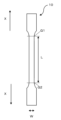
表1から表3に示す各はんだ合金それぞれについて、図1に示すような試験片10を作製した。
なお、試験片10は、中央平行部(図1のG1とG2の間)が以下となるように作製された。
・中央平行部の長さ(図1のL):12mm
・中央平行部の幅(図1のW):2mm
・中央平行部の厚み:4mm
表1から表3に示す各はんだ合金それぞれについて、図1に示すような試験片10を作製した。
なお、試験片10は、中央平行部(図1のG1とG2の間)が以下となるように作製された。
・中央平行部の長さ(図1のL):12mm
・中央平行部の幅(図1のW):2mm
・中央平行部の厚み:4mm
そして、試験片10について、以下の手順で引張試験を行った。
試験片10を、卓上形精密万能試験機(製品名:オートグラフAG-50kNX plus、(株)島津製作所製)を用いて、室温下にて、0.72mm/minのストロークで、破断するまでX方向に引っ張った。
そして、試験片10が破断したときのストローク距離をGL1、引っ張り前の試験片の中央平行部の長さLをGL0とし、以下の式に基づき、試験片10の伸び率を算出した。
伸び率(%)=(GL1-GL0)/GL0×100
1種のはんだ合金につき5本の試験片10を作製し、上記手順に従い、それぞれについて伸び率および伸び率の平均値を算出し、以下の基準に基づき評価した。その結果を表4から表6に示す。
◎:伸び率の平均値が、35%以上である
○:伸び率の平均値が、30%以上、35%未満である
△:伸び率の平均値が、25%以上、30%未満である
×:伸び率の平均値が、25%未満である
(2)落下衝撃試験
以下の各成分を混練したフラックスと、表1から表3に示すはんだ合金の粉末(粉末粒径20μmから38μm)とを、以下の配合比(質量%)にてそれぞれ混練し、各ソルダペーストを作製した。なお、はんだ合金の粉末は、アトマイズ法により作製した。
はんだ合金の粉末:フラックス=89:11
<フラックスの組成>
・水添酸変性ロジン(製品名:KE-604、荒川化学工業(株)製):49質量%
・活性剤(グルタル酸:0.3質量%、スベリン酸:2質量%、マロン酸:0.5質量%、ドデカン二酸:2質量%、ジブロモブテンジオール:2質量%)
・脂肪酸アマイド(製品名:スリパックスZHH、日本化成(株)製):6質量%
・ジエチレングリコールモノヘキシルエーテル:35.2質量%
・ヒンダードフェノール系酸化防止剤(製品名:イルガノックス245、BASFジャパン(株)製):3質量%
また、以下の用具を準備した。
・LGA(Land Grid Array、ピッチ幅:0.5mm、サイズ:縦12mm×横12mm×厚さ1mm、端子数:228ピン)
・ガラスエポキシ基板(基材:FR-4、表面処理:Cu-OSP、厚み:1.0mm、上記LGAを実装できるパターンを有するもの)
・メタルマスク(厚さ:100μm、上記パターンに対応するもの)
ソルダペーストごとに、前記ガラスエポキシ基板を5枚と、20個のLGAを使用した。
そして、上記用具および各ソルダペーストを用い、以下の手順にて、各試験基板を作製し、落下衝撃試験を行った。
・LGA(Land Grid Array、ピッチ幅:0.5mm、サイズ:縦12mm×横12mm×厚さ1mm、端子数:228ピン)
・ガラスエポキシ基板(基材:FR-4、表面処理:Cu-OSP、厚み:1.0mm、上記LGAを実装できるパターンを有するもの)
・メタルマスク(厚さ:100μm、上記パターンに対応するもの)
ソルダペーストごとに、前記ガラスエポキシ基板を5枚と、20個のLGAを使用した。
そして、上記用具および各ソルダペーストを用い、以下の手順にて、各試験基板を作製し、落下衝撃試験を行った。
まず、メタルマスクを用い、ガラスエポキシ基板上にソルダペーストを印刷した。そして、印刷されたソルダペースト上の所定の位置に、ガラスエポキシ基板1枚につき4個のLGAを載置した。なお、ソルダペーストの印刷膜厚は、メタルマスクにより調整した。
そして、LGAを載置したガラスエポキシ基板を、リフロー炉(製品名:TNV-M6110CR、(株)タムラ製作所製)を用いてリフローし、LGAと、ガラスエポキシ基板と、これらを接合する接合部とを有する試験基板を作製した。
なお、上記リフローは、プリヒートを100℃から120℃、ピーク温度を200℃、150℃以上の時間が60秒間、ピーク温度から100℃までの冷却速度を1℃から4℃/秒とした。また、酸素濃度は200±100ppmに設定した。
そして、LGAを載置したガラスエポキシ基板を、リフロー炉(製品名:TNV-M6110CR、(株)タムラ製作所製)を用いてリフローし、LGAと、ガラスエポキシ基板と、これらを接合する接合部とを有する試験基板を作製した。
なお、上記リフローは、プリヒートを100℃から120℃、ピーク温度を200℃、150℃以上の時間が60秒間、ピーク温度から100℃までの冷却速度を1℃から4℃/秒とした。また、酸素濃度は200±100ppmに設定した。
次に、作製した試験基板について、落下衝撃試験機(製品名:HDST-150J、神栄テクノロジー(株))を用い、以下の条件にて落下衝撃試験を行った。
即ち、JEDEC規格JESD22-B111に準拠して、試験基板を加速度1,500G、幅0.5msの衝撃波形が負荷される高さから繰り返し自由落下させた。落下衝撃試験中は、試験基板の各接合部の電気抵抗を常時観察し、抵抗値が1,000Ωを超えた時点で破断と判断し、破断に至るまでの落下回数を測定した。
なお、ソルダペースト1種ごとに試験基板を5つ作製し、合計20個のLGAについて、上記測定結果をワイブルプロットし、累積故障率が63.2%における落下回数を特性寿命と推定し、以下の基準にて評価した。その結果を表4から表6に示す。
◎:特性寿命が110回以上である
○:特性寿命が、90回以上、110回未満である
△:特性寿命が、70回以上、90回未満である
×:特性寿命が、70回未満である
(3)ヒートサイクル試験
以下の用具を用意した。
・チップ部品(3.2mm×1.6mm)
・ガラスエポキシ基板(基材:FR-4、表面処理:Cu-OSP、厚み:1.2mm、上記チップ部品を実装できるパターンを有するもの)
・メタルマスク(厚さ:120μm、上記パターンに対応するもの)
ソルダペーストごとに、前記ガラスエポキシ基板を3枚と、30個のチップ部品を使用した。
そして、上記用具および各ソルダペーストを用い、以下の手順にて、各試験基板を作製し、ヒートサイクル試験を行った。
以下の用具を用意した。
・チップ部品(3.2mm×1.6mm)
・ガラスエポキシ基板(基材:FR-4、表面処理:Cu-OSP、厚み:1.2mm、上記チップ部品を実装できるパターンを有するもの)
・メタルマスク(厚さ:120μm、上記パターンに対応するもの)
ソルダペーストごとに、前記ガラスエポキシ基板を3枚と、30個のチップ部品を使用した。
そして、上記用具および各ソルダペーストを用い、以下の手順にて、各試験基板を作製し、ヒートサイクル試験を行った。
まず、メタルマスクを用い、ガラスエポキシ基板上にソルダペーストを印刷した。そして、印刷されたソルダペースト上の所定の位置に、ガラスエポキシ基板1枚につき10個のチップ部品を載置した。なお、ソルダペーストの印刷膜厚は、メタルマスクにより調整した。
そして、チップ部品を載置したガラスエポキシ基板を、リフロー炉(製品名:TNV-M6110CR、(株)タムラ製作所製)を用いてリフローし、チップ部品と、ガラスエポキシ基板と、これらを接合する接合部とを有する実装基板を3枚作製した。
なお、上記リフローは、プリヒートを100℃から120℃、ピーク温度を200℃、150℃以上の時間が60秒間、ピーク温度から100℃までの冷却速度を1℃から4℃/秒とした。また、酸素濃度は200±100ppmに設定した。
そして、チップ部品を載置したガラスエポキシ基板を、リフロー炉(製品名:TNV-M6110CR、(株)タムラ製作所製)を用いてリフローし、チップ部品と、ガラスエポキシ基板と、これらを接合する接合部とを有する実装基板を3枚作製した。
なお、上記リフローは、プリヒートを100℃から120℃、ピーク温度を200℃、150℃以上の時間が60秒間、ピーク温度から100℃までの冷却速度を1℃から4℃/秒とした。また、酸素濃度は200±100ppmに設定した。
次に、冷熱衝撃試験装置(製品名:ES-76LMS、日立アプライアンス(株)製)を用い、-40℃(30分間)から125℃(30分間)を1サイクルとする設定条件にて、各実装基板を以下の通り冷熱衝撃サイクルに晒し、試験基板aからcを作製した。
a:上記冷熱衝撃サイクルを2,000サイクル繰り返す環境下に晒した試験基板
b:上記冷熱衝撃サイクルを2,250サイクル繰り返す環境下に晒した試験基板
c:上記冷熱衝撃サイクルを2,500サイクル繰り返す環境下に晒した試験基板
a:上記冷熱衝撃サイクルを2,000サイクル繰り返す環境下に晒した試験基板
b:上記冷熱衝撃サイクルを2,250サイクル繰り返す環境下に晒した試験基板
c:上記冷熱衝撃サイクルを2,500サイクル繰り返す環境下に晒した試験基板
各試験基板aからcの対象部分を切り出し、これをエポキシ樹脂(製品名:HERZOGエポ低粘度樹脂(主剤および硬化剤)、ハルツォク・ジャパン(株)製)を用いて封止した。
そして、湿式研磨機(製品名:TegraPol-25、丸本ストルアス(株)製)を用いて、各試験基板に実装された各チップ部品の中央断面が分かるような状態とし、走査電子顕微鏡(製品名:TM-1000、(株)日立ハイテクノロジーズ製)を用いて、各試験基板aからc上の各接合部の状態を観察し、接合部を完全に横断しているクラックの有無を確認し、以下の基準に従い評価した。その結果を表4から表6に示す。
◎:試験基板aからcの全てにおいて、接合部を完全に横断するクラックは発生しなかった
○:試験基板aおよびbにおいて、接合部を完全に横断するクラックは発生しなかった
△:試験基板aにおいて、接合部を完全に横断するクラックは発生しなかった
×:試験基板aからcの全てにおいて、接合部を完全に横断するクラックが発生した
(5)リフトオフ発生確認試験
以下の用具を用意した。
・コネクタ部品(製品名:S15B-EH(LF)(SN)、日本圧着端子製造(株)製)
・ガラスエポキシ基板(基材:FR-4、表面処理:Cu-OSP、サイズ:50mm×50mm、厚み:1.6mm、2.5mmピッチ間隔で、直径1.6ランドと直径1.0mmのスルーホールを有する)
・5mmピッチ間隔で、直径3mmの開口パターンを有する厚さ200μmのメタルマスク
そして、上記用具および各ソルダペーストを用い、以下の手順にて、各試験基板を作製し、リフトオフ発生確認試験を行った。
以下の用具を用意した。
・コネクタ部品(製品名:S15B-EH(LF)(SN)、日本圧着端子製造(株)製)
・ガラスエポキシ基板(基材:FR-4、表面処理:Cu-OSP、サイズ:50mm×50mm、厚み:1.6mm、2.5mmピッチ間隔で、直径1.6ランドと直径1.0mmのスルーホールを有する)
・5mmピッチ間隔で、直径3mmの開口パターンを有する厚さ200μmのメタルマスク
そして、上記用具および各ソルダペーストを用い、以下の手順にて、各試験基板を作製し、リフトオフ発生確認試験を行った。
まず、メタルマスクを用い、ガラスエポキシ基板上にソルダペーストを印刷した。そして、ガラスエポキシ基板に設けられた所定のスルーホール内にコネクタ部品の端子をそれぞれ挿入し、リフロー炉(製品名:TNP-538EM、(株)タムラ製作所製)を用いてリフローし、コネクタ部品と、ガラスエポキシ基板とを接合するはんだ接合部(フィレット)とを有する試験基板を作製した。なお、上記リフローは、(2)落下衝撃試験と同じ条件にて行った。
次いで、各試験基板の対象部分を切り出し、これをエポキシ樹脂(製品名:エポマウント(主剤及び硬化剤)、リファインテック(株)製)を用いて封止した。更に湿式研磨機(製品名:TegraPol-25、丸本ストルアス(株)製)を用いて各試験基板に実装された各コネクタ部品の端子の中央断面が分かるような状態とし、走査電子顕微鏡(製品名:TM-1000、(株)日立ハイテクノロジーズ製)を用いて観察し、以下の基準に従い評価した。なお、評価端子数は8個とした。その結果を表4から表6に示す。
○:リフトオフ発生せず
×:リフトオフ発生
○:リフトオフ発生せず
×:リフトオフ発生
(5)針状物質発生確認試験
各はんだ合金からなるはんだインゴットを作成した。そして、各はんだインゴットについて、以下の条件に基づき、はんだ合金粉末を作成した。
まず、2Lのステンレスビーカーに、50gのはんだインゴットと、890gのヒマシ油と、10gの水添酸変性ロジン(製品名:KE-604、荒川化学工業(株)製)とを入れた。そして、これをマントルヒーターを用いて、継続的に加熱した。
ステンレスビーカー内の収容物の温度が100℃に達した時点で、ホモジナイザー((株)エスエムテー製)を使用し、回転数を2,000rpmに設定して、ステンレスビーカー内の収容物の攪拌を開始した。なお、攪拌中も、マントルヒーターによる加熱は継続した。
そして、ステンレスビーカー内の収容物の温度が200℃に到達した時点で、加熱を停止し、ホモジナイザーの回転を10,000rpmに変更して、その後、5分間、ステンレスビーカー内の収容物を撹拌した。攪拌終了後、ステンレスビーカー内の収容物の温度が室温になるまで冷却した。
そして、ステンレスビーカー内から、ヒマシ油中に沈降したはんだ合金粉末を取り出し、これを酢酸エチルで洗浄して付着物を取り除いた後、はんだ合金粉末の状態をデジタルマイクロスコープを用いて、200倍で観察した。その観察結果を、以下の基準に基づき評価した。その結果を表4から表6に示す。
○:はんだ合金粉末に針状物質は発生していない
×:はんだ合金粉末に針状物質が発生した


以上の通り、本実施例のはんだ合金は、Bi、Sb、AgおよびSnを所定量含むことにより、Biを含みつつ、上記(1)から(4)のいずれにおいても、良好な結果を示す接合部を形成できる。また、本実施例のはんだ合金は、Feを添加した場合でも、針状物質の生成を抑制できる。
ここで、自動車が対象物に衝突した際のひずみ速度は、10-3(s-1)から103(s-1)と言われている。そして、(1)引張試験においては、GL0が12mmの試験片を0.72mm/minのストロークで引っ張っているため、これをひずみ速度に換算すると、10―3(s-1)となる。
このように、本実施例のはんだ合金は、自動車が対象物に衝突した際のひずみ速度に匹敵するような負荷を与えた場合においても、良好な耐性、即ち、良好な強度と延性とを有する接合部を形成できることが分かる。
ここで、自動車が対象物に衝突した際のひずみ速度は、10-3(s-1)から103(s-1)と言われている。そして、(1)引張試験においては、GL0が12mmの試験片を0.72mm/minのストロークで引っ張っているため、これをひずみ速度に換算すると、10―3(s-1)となる。
このように、本実施例のはんだ合金は、自動車が対象物に衝突した際のひずみ速度に匹敵するような負荷を与えた場合においても、良好な耐性、即ち、良好な強度と延性とを有する接合部を形成できることが分かる。
このように、本実施例のはんだ合金は、Biを含みつつ、ヒートサイクル耐性および耐落下衝撃性を有しリフトオフの発生を抑制できる接合部を形成することができる。また、このような接合部を有する電子制御装置および電子機器は、高い信頼性を発揮することができる。
10 試験片
Claims (10)
- 35質量%以上65質量%以下のBiと、0.1質量%以上0.65質量%以下のSbと、0.05質量%以上2質量%以下のAgとを含み、残部がSnと不可避不純物とからなる、はんだ合金。
- 更に、P、GaおよびGeの群から選ばれる1種以上を合計で0.001質量%以上0.05質量%以下含む、請求項1に記載のはんだ合金。
- 更に、Mn、Ti、Al、Cr、V、Fe、Mg、Pd、PbおよびMoの群から選ばれる1種以上を合計で0.001質量%以上0.05質量%以下含む、請求項1または請求項2に記載のはんだ合金。
- 請求項1から請求項3のいずれか1項に記載のはんだ合金を含む、接合材。
- 粉末状である請求項1から請求項3のいずれか1項に記載のはんだ合金と、
ベース樹脂と、チクソ剤と、活性剤と、溶剤とを含むフラックスとを含む、ソルダペースト。 - 請求項1から請求項3のいずれか1項に記載のはんだ合金で形成された、接合部。
- 請求項4に記載の接合材で形成された、接合部。
- 請求項5に記載のソルダペーストで形成された、接合部。
- 第1の被接合材と、接合部と、第2の被接合材とを有し、
前記接合部は、請求項6から請求項8のいずれか1項に記載の接合部であり、
前記第1の被接合材と、前記第2の被接合材とは、前記接合部を介して接合されている、接合構造体。 - 請求項9に記載の接合構造体を有する、電子制御装置。
Priority Applications (3)
| Application Number | Priority Date | Filing Date | Title |
|---|---|---|---|
| PCT/JP2023/002160 WO2024157366A1 (ja) | 2023-01-24 | 2023-01-24 | はんだ合金、接合部、接合材、ソルダペースト、接合構造体および電子制御装置 |
| CN202380016098.7A CN118748957A (zh) | 2023-01-24 | 2023-01-24 | 软钎料合金、接合部、接合材料、焊膏、接合结构体和电子控制装置 |
| JP2023505858A JP7262695B1 (ja) | 2023-01-24 | 2023-01-24 | はんだ合金、接合部、接合材、ソルダペースト、接合構造体および電子制御装置 |
Applications Claiming Priority (1)
| Application Number | Priority Date | Filing Date | Title |
|---|---|---|---|
| PCT/JP2023/002160 WO2024157366A1 (ja) | 2023-01-24 | 2023-01-24 | はんだ合金、接合部、接合材、ソルダペースト、接合構造体および電子制御装置 |
Publications (1)
| Publication Number | Publication Date |
|---|---|
| WO2024157366A1 true WO2024157366A1 (ja) | 2024-08-02 |
Family
ID=86052921
Family Applications (1)
| Application Number | Title | Priority Date | Filing Date |
|---|---|---|---|
| PCT/JP2023/002160 WO2024157366A1 (ja) | 2023-01-24 | 2023-01-24 | はんだ合金、接合部、接合材、ソルダペースト、接合構造体および電子制御装置 |
Country Status (3)
| Country | Link |
|---|---|
| JP (1) | JP7262695B1 (ja) |
| CN (1) | CN118748957A (ja) |
| WO (1) | WO2024157366A1 (ja) |
Citations (5)
| Publication number | Priority date | Publication date | Assignee | Title |
|---|---|---|---|---|
| JP2001334386A (ja) * | 2000-05-19 | 2001-12-04 | Hitachi Ltd | 電子機器用Sn−Ag−Bi系はんだ |
| CN102029479A (zh) * | 2010-12-29 | 2011-04-27 | 广州有色金属研究院 | 一种低银无铅焊料合金及其制备方法和装置 |
| JP2017051984A (ja) * | 2015-09-10 | 2017-03-16 | 株式会社弘輝 | はんだ合金及びはんだ組成物 |
| WO2019171978A1 (ja) * | 2018-03-08 | 2019-09-12 | 千住金属工業株式会社 | はんだ合金、はんだペースト、はんだボール、やに入りはんだおよびはんだ継手 |
| WO2020209384A1 (ja) * | 2019-04-11 | 2020-10-15 | 株式会社日本スペリア社 | 鉛フリーはんだ合金及びはんだ接合部 |
-
2023
- 2023-01-24 WO PCT/JP2023/002160 patent/WO2024157366A1/ja unknown
- 2023-01-24 JP JP2023505858A patent/JP7262695B1/ja active Active
- 2023-01-24 CN CN202380016098.7A patent/CN118748957A/zh active Pending
Patent Citations (5)
| Publication number | Priority date | Publication date | Assignee | Title |
|---|---|---|---|---|
| JP2001334386A (ja) * | 2000-05-19 | 2001-12-04 | Hitachi Ltd | 電子機器用Sn−Ag−Bi系はんだ |
| CN102029479A (zh) * | 2010-12-29 | 2011-04-27 | 广州有色金属研究院 | 一种低银无铅焊料合金及其制备方法和装置 |
| JP2017051984A (ja) * | 2015-09-10 | 2017-03-16 | 株式会社弘輝 | はんだ合金及びはんだ組成物 |
| WO2019171978A1 (ja) * | 2018-03-08 | 2019-09-12 | 千住金属工業株式会社 | はんだ合金、はんだペースト、はんだボール、やに入りはんだおよびはんだ継手 |
| WO2020209384A1 (ja) * | 2019-04-11 | 2020-10-15 | 株式会社日本スペリア社 | 鉛フリーはんだ合金及びはんだ接合部 |
Also Published As
| Publication number | Publication date |
|---|---|
| CN118748957A (zh) | 2024-10-08 |
| JP7262695B1 (ja) | 2023-04-21 |
Similar Documents
| Publication | Publication Date | Title |
|---|---|---|
| US10926360B2 (en) | Lead-free solder alloy, solder joint, solder paste composition, electronic circuit board, and electronic device | |
| JP6755837B2 (ja) | 鉛フリーはんだ合金、電子回路基板および電子制御装置 | |
| JP6230737B1 (ja) | 鉛フリーはんだ合金、ソルダペースト及び電子回路基板 | |
| WO2009104693A1 (ja) | はんだ接合構造およびはんだ付け用フラックス | |
| JP6560272B2 (ja) | ソルダペースト、電子回路基板及び電子制御装置 | |
| JP6363307B2 (ja) | フラックス組成物、ソルダペースト組成物及び電子回路基板 | |
| JP6585554B2 (ja) | 鉛フリーはんだ合金、電子回路基板及び電子制御装置 | |
| WO2019167705A1 (ja) | 鉛フリーはんだ合金、電子回路実装基板及び電子制御装置 | |
| WO2023243108A1 (ja) | はんだ合金、接合部、接合材、ソルダペースト、接合構造体および制御装置 | |
| WO2024157366A1 (ja) | はんだ合金、接合部、接合材、ソルダペースト、接合構造体および電子制御装置 | |
| JP6619387B2 (ja) | 鉛フリーはんだ合金 | |
| JP7406052B1 (ja) | はんだ合金、ソルダペースト、接合部、接合構造体および電子制御装置 | |
| WO2023243104A1 (ja) | はんだ合金、接合部、接合材、ソルダペースト、接合構造体および制御装置 | |
| WO2024042663A1 (ja) | はんだ合金、接合部、接合材、ソルダペースト、接合構造体および電子制御装置 | |
| JP6916243B2 (ja) | 鉛フリーはんだ合金、電子回路基板及び電子制御装置 | |
| JP2018122322A (ja) | 鉛フリーはんだ合金、ソルダペースト、電子回路基板及び電子制御装置 | |
| JP6420936B1 (ja) | 鉛フリーはんだ合金、ソルダペースト、電子回路実装基板及び電子制御装置 | |
| JP4662483B2 (ja) | 導電性フィラー、及び中温はんだ材料 | |
| JP2024062898A (ja) | はんだ合金、ソルダペースト、プリント回路基板及び電子制御装置 | |
| JP2019209350A (ja) | 鉛フリーはんだ合金、ソルダペースト、電子回路実装基板及び電子制御装置 | |
| JP6795630B2 (ja) | 鉛フリーはんだ合金、ソルダペースト組成物、電子回路基板および電子制御装置 | |
| CN116833616A (zh) | 无铅软钎料合金、焊膏、电子电路安装基板和电子控制装置 |
Legal Events
| Date | Code | Title | Description |
|---|---|---|---|
| 121 | Ep: the epo has been informed by wipo that ep was designated in this application |
Ref document number: 23918333 Country of ref document: EP Kind code of ref document: A1 |