WO2024079846A1 - 電力半導体装置および電力半導体装置の製造方法 - Google Patents
電力半導体装置および電力半導体装置の製造方法 Download PDFInfo
- Publication number
- WO2024079846A1 WO2024079846A1 PCT/JP2022/038210 JP2022038210W WO2024079846A1 WO 2024079846 A1 WO2024079846 A1 WO 2024079846A1 JP 2022038210 W JP2022038210 W JP 2022038210W WO 2024079846 A1 WO2024079846 A1 WO 2024079846A1
- Authority
- WO
- WIPO (PCT)
- Prior art keywords
- heat sink
- semiconductor device
- housing
- structural support
- power semiconductor
- Prior art date
- Legal status (The legal status is an assumption and is not a legal conclusion. Google has not performed a legal analysis and makes no representation as to the accuracy of the status listed.)
- Ceased
Links
Images



















Classifications
-
- H—ELECTRICITY
- H10—SEMICONDUCTOR DEVICES; ELECTRIC SOLID-STATE DEVICES NOT OTHERWISE PROVIDED FOR
- H10W—GENERIC PACKAGES, INTERCONNECTIONS, CONNECTORS OR OTHER CONSTRUCTIONAL DETAILS OF DEVICES COVERED BY CLASS H10
- H10W40/00—Arrangements for thermal protection or thermal control
- H10W40/20—Arrangements for cooling
- H10W40/22—Arrangements for cooling characterised by their shape, e.g. having conical or cylindrical projections
- H10W40/226—Arrangements for cooling characterised by their shape, e.g. having conical or cylindrical projections characterised by projecting parts, e.g. fins to increase surface area
- H10W40/228—Arrangements for cooling characterised by their shape, e.g. having conical or cylindrical projections characterised by projecting parts, e.g. fins to increase surface area the projecting parts being wire-shaped or pin-shaped
-
- H—ELECTRICITY
- H10—SEMICONDUCTOR DEVICES; ELECTRIC SOLID-STATE DEVICES NOT OTHERWISE PROVIDED FOR
- H10W—GENERIC PACKAGES, INTERCONNECTIONS, CONNECTORS OR OTHER CONSTRUCTIONAL DETAILS OF DEVICES COVERED BY CLASS H10
- H10W40/00—Arrangements for thermal protection or thermal control
- H10W40/60—Securing means for detachable heating or cooling arrangements, e.g. clamps
-
- H—ELECTRICITY
- H10—SEMICONDUCTOR DEVICES; ELECTRIC SOLID-STATE DEVICES NOT OTHERWISE PROVIDED FOR
- H10W—GENERIC PACKAGES, INTERCONNECTIONS, CONNECTORS OR OTHER CONSTRUCTIONAL DETAILS OF DEVICES COVERED BY CLASS H10
- H10W40/00—Arrangements for thermal protection or thermal control
- H10W40/60—Securing means for detachable heating or cooling arrangements, e.g. clamps
- H10W40/611—Bolts or screws
Definitions
- This disclosure relates to a power semiconductor device equipped with a heat sink and a power module, and a method for manufacturing the same.
- Patent document 1 describes a heat dissipation device in which multiple modular cooling devices, each equipped with a heat dissipation plate on which a heat generating element is arranged, are inserted into an opening in the housing and held by the housing.
- the present disclosure has been made in consideration of the above, and aims to obtain a power semiconductor device that can suppress bending of a holding portion to which multiple power modules and a heat sink are attached.
- the power semiconductor device includes a heatsink-integrated power module in which a power module and a heatsink that dissipates heat generated by the power module and has multiple heat dissipation fins provided on a heatsink base are integrated, a box-shaped holding section having an air inlet and an air outlet provided opposite each other and multiple openings formed on one side connecting the inlet and the outlet, and a structural support section provided inside the holding section and supporting one side by receiving a load from the one side toward the inside of the holding section.
- the multiple heatsink-integrated power modules have multiple heat dissipation fins inserted into the holding section from the openings, and the outer peripheral edge of the heatsink base is supported on an adjacent region adjacent to the opening on one side in the in-plane direction of the heatsink base.
- the structural support section is disposed at a position corresponding to between the heatsink bases of adjacent heatsink-integrated power modules in the width direction of the holding section, which is a direction perpendicular to the direction from the inlet to the outlet.
- the power semiconductor device disclosed herein has the advantage of being able to suppress bending of the holding portion to which multiple power modules and heat sinks are attached.
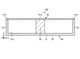
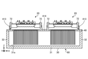
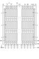
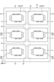
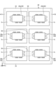
- FIG. 1 is a plan view showing a configuration of a power semiconductor device according to a first embodiment
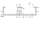
- FIG. 2 is a first cross-sectional view showing the configuration of the power semiconductor device according to the first embodiment, taken along line II-II in FIG.
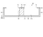
- FIG. 3 is a second cross-sectional view showing the configuration of the power semiconductor device according to the first embodiment, taken along line III-III in FIG. 1 is a cross-sectional view of a heat sink-integrated power module according to a first embodiment
- FIG. 1 is a cross-sectional view of a heat sink-integrated power module of a first modified example to which a heat sink of a first modified example according to a first embodiment is attached;
- FIG. 1 is a plan view showing a configuration of a power semiconductor device according to a first embodiment
- FIG. 2 is a first cross-sectional view showing the configuration of the power semiconductor device according to the first embodiment, taken along line II-II in FIG.
- FIG. 3 is a second cross-sectional view showing the
- FIG. 11 is a cross-sectional view of a heat sink-integrated power module according to a second modified example to which a heat sink according to a second modified example of the first embodiment is attached; 13 is a cross-sectional view of a heat sink-integrated power module according to a third modified example of the first embodiment;
- FIG. 1 is a top view showing an outer frame of a power semiconductor device according to a first embodiment;
- FIG. 9 is a cross-sectional view showing an outer frame of the power semiconductor device according to the first embodiment, taken along line IX-IX in FIG.
- FIG. 1 is a top view showing a housing of a power semiconductor device according to a first embodiment;
- FIG. 1 is a first top view diagrammatically illustrating an example of a procedure for a method for manufacturing a power semiconductor device according to a first embodiment
- 1 is a first cross-sectional view showing an example of a procedure of a method for manufacturing a power semiconductor device according to a first embodiment of the present invention
- FIG. FIG. 2 is a second top view diagrammatically illustrating an example of a procedure of the method for manufacturing the power semiconductor device according to the first embodiment
- 2 is a second cross-sectional view showing an example of a procedure of the method for manufacturing the power semiconductor device according to the first embodiment
- FIG. 3 is a third cross-sectional view illustrating an example of a procedure of the method for manufacturing the power semiconductor device according to the first embodiment
- FIG. 3 is a third top view diagrammatically illustrating an example of a procedure of the method for manufacturing the power semiconductor device according to the first embodiment
- FIG. 4 is a fourth top view diagrammatically illustrating an example of a procedure of the method for manufacturing the power semiconductor device according to the first embodiment
- FIG. 5 is a fifth top view diagrammatically illustrating an example of a procedure of the method for manufacturing the power semiconductor device according to the first embodiment
- 1 is a flowchart showing the steps of a method for manufacturing a power semiconductor device according to a first embodiment.
- FIG. 1 is a first schematic diagram illustrating an example of a size relationship between an opening of a housing and a heat sink base of a heat sink-integrated power module in a power semiconductor device according to a first embodiment;
- FIG. 1 is a first schematic diagram illustrating an example of a size relationship between an opening of a housing and a heat sink base of a heat sink-integrated power module in a power semiconductor device according to a first embodiment;
- FIG. 1 is
- FIG. 2 is a second schematic diagram illustrating an example of a size relationship between an opening of a housing and a heat sink base of a heat sink-integrated power module in the power semiconductor device according to the first embodiment
- FIG. 3 is a third schematic diagram illustrating an example of a size relationship between an opening of a housing and a heat sink base of a heat sink-integrated power module in the power semiconductor device according to the first embodiment
- FIG. 1 is a first cross-sectional view showing a method for manufacturing a power semiconductor device according to a comparative example of the first embodiment
- FIG. 2 is a second cross-sectional view showing the manufacturing method of the power semiconductor device of the comparative example according to the first embodiment
- FIG. 1 is a schematic diagram illustrating an air flow inside a holding portion in a power semiconductor device according to a first embodiment
- FIG. 13 is a schematic diagram illustrating an air flow inside a holding portion in a power semiconductor device of a comparative example according to the first embodiment
- FIG. 1 is a first cross-sectional view showing an example of a method for fixing a structural support portion to an outer frame in a power semiconductor device according to a first embodiment
- FIG. 4 is a second cross-sectional view showing an example of a method for fixing a structural support portion to an outer frame in the power semiconductor device according to the first embodiment
- FIG. 11 is a third cross-sectional view showing an example of a method for fixing a structural support portion to an outer frame in the power semiconductor device according to the first embodiment
- FIG. 1 is a first cross-sectional view showing an example of a method for fixing a structural support portion to an outer frame in a power semiconductor device according to a first embodiment
- FIG. 4 is a second cross-sectional view showing
- FIG. 4 is a fourth cross-sectional view showing an example of a method for fixing a structural support portion to an outer frame in the power semiconductor device according to the first embodiment
- FIG. 4 is a first cross-sectional view showing an example of a method for fixing a structural support portion to a housing in the power semiconductor device according to the first embodiment
- FIG. 5 is a second cross-sectional view showing an example of a method for fixing the structural support portion to the housing in the power semiconductor device according to the first embodiment
- 1 is a flowchart showing the steps of another method for manufacturing a power semiconductor device according to a first embodiment.
- FIG. 1 is a first cross-sectional view showing a structure of a power semiconductor device in which a structural support part with an elastic function is applied to the power semiconductor device according to a first embodiment
- FIG. 2 is a second cross-sectional view showing the structure of the power semiconductor device when the elastic structural support portion is applied to the power semiconductor device according to the first embodiment
- FIG. 1 is a first cross-sectional view illustrating a positional relationship between a structural support portion, a heat sink base of a heat sink-integrated power module, and a housing in a power semiconductor device according to a first embodiment
- FIG. 2 is a second cross-sectional view illustrating a relationship between a structural support portion, a heat sink base of a heat sink-integrated power module, and a housing in the power semiconductor device according to the first embodiment
- FIG. 11 is a third cross-sectional view illustrating a relationship between a structural support portion, a heat sink base of a heat sink-integrated power module, and a housing in the power semiconductor device according to the first embodiment
- FIG. 1 is a first top view illustrating a shape and arrangement of a structural support portion in a power semiconductor device according to a first embodiment
- FIG. 4 is a second top view illustrating the shape and arrangement of the structural support portion in the power semiconductor device according to the first embodiment
- FIG. 4 is a third top view illustrating the shape and arrangement of the structural support portion in the power semiconductor device according to the first embodiment;
- FIG. 4 is a fourth top view illustrating the shape and arrangement of the structural support portion in the power semiconductor device according to the first embodiment;
- FIG. 11 is a cross-sectional view showing a configuration of a power semiconductor device according to a second embodiment.
- FIG. 11 is a cross-sectional view showing a configuration of a power semiconductor device according to a second embodiment.
- FIG. 11 is a cross-sectional view showing a configuration of a heat sink-integrated power module according to a third embodiment.
- FIG. 11 is a cross-sectional view showing a configuration of a power semiconductor device according to a third embodiment.
- Fig. 1 is a plan view showing a configuration of a power semiconductor device 100 according to a first embodiment.
- Fig. 2 is a first cross-sectional view showing the configuration of the power semiconductor device 100 according to the first embodiment, which is a cross-sectional view taken along line II-II in Fig. 1.
- Fig. 3 is a second cross-sectional view showing the configuration of the power semiconductor device 100 according to the first embodiment, which is a cross-sectional view taken along line III-III in Fig. 1. Note that some hatching has been omitted from the cross-sectional view to make it easier to see.
- the left-right direction in FIG. 1 to FIG. 3 is the left-right direction of the power semiconductor device 100 and the components of the power semiconductor device 100.
- the left-right direction corresponds to the X direction in FIG. 1 to FIG. 3 and corresponds to the width direction of the power semiconductor device 100 and the components of the power semiconductor device 100.
- the depth direction of the paper in FIG. 2 and FIG. 3 and the up-down direction in FIG. 1 are the depth direction of the power semiconductor device 100 and the components of the power semiconductor device 100.
- the depth direction corresponds to the Y direction in FIG. 1 to FIG. 3 and corresponds to the depth direction of the power semiconductor device 100 and the components of the power semiconductor device 100.
- the depth direction can be rephrased as the traveling direction of the air flow 200 blown from the blowing system (not shown) to the power semiconductor device 100, that is, the blowing direction or the wind inflow direction in the power semiconductor device 100.
- the depth direction can be rephrased as the traveling direction of the air flow 200 inside the holding portion 60.
- the up-down direction in FIG. 2 and FIG. 3 and the depth direction of the paper in FIG. 1 are the up-down direction of the power semiconductor device 100 and the components of the power semiconductor device 100.
- the up-down direction corresponds to the Z direction in Figures 1 to 3, and corresponds to the height direction of the power semiconductor device 100 and the components of the power semiconductor device 100.
- the near side in the depth direction of the paper of Figures 2 and 3, and the lower side of Figure 1 are the front sides of the power semiconductor device 100 and the heat sink integrated power module 20.
- the far side in the depth direction of the paper of Figures 2 and 3, and the upper side of Figure 1 are the rear sides of the power semiconductor device 100 and the heat sink integrated power module 20.
- the power semiconductor device 100 has multiple heat sink integrated power modules 20 mounted on a holding portion 60.
- the power semiconductor device 100 includes multiple heat sink integrated power modules 20, a structural support portion 50, and a holding portion 60.
- FIG. 1 shows a power semiconductor device 100 mounted with six heat sink integrated power modules 20 arranged in two columns and three rows, as an example of a power semiconductor device mounted with multiple heat sink integrated power modules 20 according to the first embodiment.
- the holding portion 60 houses and holds a portion of the multiple heat sink integrated power modules 20 in the power semiconductor device 100. That is, the multiple heat sink integrated power modules 20 are held in the holding portion 60 with a portion of each module housed in the holding portion 60.
- the holding portion 60 is composed of a housing 40 and an outer frame 30.
- the heatsink-integrated power modules 20, namely, heatsink-integrated power module 20a, heatsink-integrated power module 20b, heatsink-integrated power module 20c, heatsink-integrated power module 20d, heatsink-integrated power module 20e, and heatsink-integrated power module 20f, are attached to a holding portion 60.
- the number of heatsink-integrated power modules 20 attached to the power semiconductor device 100 is not limited to six.
- two or more heatsink-integrated power modules 20 may be attached to the holding portion 60 in the left-right direction. Even in this configuration, the effects of the power semiconductor device 100 described below can be obtained.
- the air flow 200 blown from the ventilation system flows from the front side to the rear side. Note that the direction in which the air flow 200 flows may also be from the rear side to the front side.
- the heat sink integrated power module 20 is a power semiconductor module mounted on the power semiconductor device 100, and is a resin molded type power module.
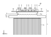
- FIG. 4 is a cross-sectional view of the heat sink integrated power module 20 according to the first embodiment.
- the heat sink integrated power module 20 according to the first embodiment includes a heat sink 1, a fin base 2, an insulating sheet 3, wiring wires 4, a semiconductor element 5, solder 6, a metal conductor 7, a control terminal 8, a sealing resin 9, and a main terminal 10.
- the heat sink 1 also has a plurality of heat dissipation fins 1a and a heat sink base 1b.
- the power module 11 according to the first embodiment is composed of the insulating sheet 3, wiring wires 4, semiconductor element 5, solder 6, metal conductor 7, control terminal 8, sealing resin 9 and main terminal 10. Therefore, the heat sink integrated power module 20 according to the first embodiment is composed of the heat sink 1 and the power module 11 joined via the fin base 2. That is, the heat sink integrated power module 20 is composed of the power module 11 and the heat sink 1, which has a plurality of heat dissipation fins 1a provided on the heat sink base 1b and dissipates heat generated by the power module 11, which are integrated together.
- the heat sink integrated power module 20 has a heat sink 1 connected to the underside of the power module 11, improving the dissipation of heat generated in the semiconductor element 5 of the power module 11. That is, the heat sink integrated power module 20 improves the dissipation of heat generated in the power module 11 by dissipating heat generated in the semiconductor element 5 of the power module 11 from the heat sink 1.
- the heat sink integrated power module 20 is a greaseless power module that does not use thermally conductive grease between the power module 11 and the heat sink 1. Therefore, the heat sink integrated power module 20 has improved heat dissipation characteristics for heat generated in the power module 11 compared to when thermally conductive grease is used between the power module 11 and the heat sink 1, and has higher heat dissipation performance.
- the heat sink 1 is a crimped heat sink in which the heat dissipation fins 1a and the heat sink base 1b are integrated by crimping.
- the heat dissipation fin 1a is a thin plate-like heat dissipation component having a rectangular shape.
- the heat dissipation fin 1a is made of a metal material with relatively high thermal conductivity so that it can dissipate heat generated in the semiconductor element 5 of the power module 11.
- the heat dissipation fin 1a is made of a metal material that is resistant to corrosion, such as aluminum or an aluminum alloy.
- Each of the multiple heat dissipation fins 1a is inserted into a fin insertion groove (not shown) formed on one side of the heat sink base 1b and is fixed to the heat sink base 1b by crimping.
- the heat dissipation fins 1a are arranged so that the heat sink base 1b is sandwiched between the fin base 2.
- the heat sink base 1b is a flat part having a rectangular shape in the in-plane direction of the heat sink base 1b, and is a part to which a plurality of heat dissipation fins 1a are fixed, forming the base of the heat sink 1.
- the heat sink base 1b is made of a metal material with relatively high thermal conductivity so that heat generated in the semiconductor element 5 of the power module 11 can be efficiently transferred to the heat dissipation fins 1a.
- the heat sink base 1b is made of a metal material that is resistant to corrosion, such as aluminum and aluminum alloys.
- the heat sink base 1b is manufactured by a processing method such as cutting, die casting, forging, and extrusion.
- the fin base 2 is a flat rectangular plate-like part smaller than the heat sink base 1b, and is a connecting part that connects the power module 11 and the heat sink 1.
- the fin base 2 is made of a metal material with relatively high thermal conductivity so that heat generated in the semiconductor element 5 of the power module 11 can be efficiently transferred from the power module 11 to the heat sink 1.
- the fin base 2 is made of a metal material that is resistant to corrosion, such as aluminum or an aluminum alloy.
- the fin base 2 is manufactured by a processing method such as cutting, die casting, forging, or extrusion.
- the materials of the heat dissipation fins 1a, heat sink base 1b, and fin base 2 are not limited to the aluminum-based materials described above, and may be other materials.
- the combination of materials of the heat dissipation fins 1a, heat sink base 1b, and fin base 2 may be a combination of materials different from those described above.
- the heat dissipation capacity of the heat dissipation fins 1a is improved even more than when the heat dissipation fins 1a are plate components made of an aluminum-based material.
- the heat sink 1 When a crimped heat sink in which the heat dissipation fins 1a and the heat sink base 1b are integrated by crimping is used for the heat sink 1, there are no processing restrictions on the aspect ratio that exist when producing a heat sink by die casting or extrusion, so the heat dissipation fins 1a can be designed freely and the heat dissipation capacity of the heat sink 1 can be improved.
- the heat sink 1 is not limited to a crimped heat sink, and heat sinks produced by other processing methods may also be used.
- FIG. 5 is a cross-sectional view of a heat sink-integrated power module of a first modified example to which a heat sink 12 of a first modified example according to embodiment 1 is attached.
- the same components as in FIG. 4 are given the same reference numerals.
- the heat dissipation fins 1a and the heat sink base 1b are integrally manufactured by extrusion processing.
- FIG. 6 is a cross-sectional view of a heat sink-integrated power module of a second modified example to which a heat sink 13 of a second modified example according to the first embodiment is attached.
- the same components as in FIG. 4 are given the same reference numerals.
- the heat dissipation fins 1a and the heat sink base 1b are integrally produced by die casting.
- a heat sink made by cutting or forging may be used.
- FIG. 7 is a cross-sectional view of a heat sink-integrated power module of a third modified example according to the first embodiment.
- the power module 11 and the heat sink 1 are connected by a bonding material 15 such as solder or an adhesive 16.
- the insulating sheet 3 insulates the components sealed in the sealing resin 9 from the heat sink base 1b, and dissipates heat generated by the semiconductor element 5 to the heat sink base 1b.
- the insulating sheet 3 has heat dissipation properties equal to or greater than those of the sealing resin 9.
- the wiring wires 4 electrically connect the semiconductor elements 5 to each other and also electrically connect the semiconductor elements 5 to the main terminals 10.
- the semiconductor element 5 is a semiconductor element for power control.
- Examples of the semiconductor element 5 are a rectifier diode, a power transistor, a thyristor, and an IGBT (Insulated Gate Bipolar Transistor).
- the semiconductor element 5 is exemplified by an element formed of silicon (Si), or an element formed of a wide band gap semiconductor having a larger band gap than silicon. Examples of wide band gap semiconductors are silicon carbide (SiC), gallium nitride-based materials, and diamond.
- the semiconductor element 5 using a wide band gap semiconductor has a high allowable current density and low power loss, and therefore the heat sink-integrated power module 20 and the power semiconductor device 100 can be made smaller.
- the solder 6 is a bonding material that bonds the semiconductor element 5 and the metal conductor 7. Note that the bonding material that bonds the semiconductor element 5 and the metal conductor 7 is not limited to the solder 6.
- the metal conductor 7 is a substrate on which the semiconductor element 5 is mounted, and dissipates heat generated by the semiconductor element 5 to the insulating sheet 3.
- the control terminal 8 and the main terminal 10 are connected to the semiconductor element 5 to supply power to the semiconductor element 5 or transmit signals between the semiconductor element 5 and an external device.
- the sealing resin 9 constitutes the housing of the power module 11.
- the sealing resin 9 is made of a thermosetting resin such as epoxy, and ensures insulation between the components arranged inside.
- the sealing resin 9 is a transfer mold formed by transfer molding, for example.
- the molding method of the sealing resin 9 is not limited to transfer molding.
- the semiconductor element 5 is die-bonded to the metal conductor 7 using solder 6.
- the semiconductor element 5 is wire-bonded to other semiconductor elements 5 by wiring wires 4, and electrically connected.
- some of the semiconductor elements 5 are wire-bonded to the control terminals 8 or the main terminals 10 by wiring wires 4, and electrically connected.
- the insulating sheet 3 is temporarily attached onto one surface of the fin base 2.
- the fin base uneven portion 2u provided on the other side of the fin base 2 and the heat sink base uneven portion 1bu provided on one side of the heat sink base 1b are fitted and fixed by press processing, thereby integrating the assembly with the heat sink base 1b.
- the fin base 2 and the heat sink base 1b are integrated by pressing, so there is concern that problems such as damage to the semiconductor element 5 during pressing, cracking of the semiconductor element 5, changes in the characteristics of the semiconductor element 5, cracking of the sealing resin 9, a decrease in the pressure resistance of the insulating sheet 3, and peeling between the various components of the heat sink integrated power module 20 may occur.
- the press load when integrating the assembly and the heat sink base 1b is as low as possible.
- FIG. 8 is a top view showing the outer frame 30 of the power semiconductor device 100 according to the first embodiment.
- FIG. 9 is a cross-sectional view showing the outer frame 30 of the power semiconductor device 100 according to the first embodiment, taken along line IX-IX in FIG. 8.
- the outer frame 30 supports the housing 40 to which the heat sink-integrated power module 20 is attached, and forms an air passage for the air flow 200 blown from the air blowing system.
- the outer frame 30 has two side sections 32 rising vertically upward from both left and right ends of the bottom surface 31 of the outer frame 30, and has a rectangular box shape with the top, front and back sides open. That is, as shown in Figures 2, 3, 8 and 9, the outer frame 30 has a U-shaped cross section in the left and right direction, and has a structure in which all sides except the top, front and back sides to which the housing 40 is attached are closed. Note that the outer frame 30 does not necessarily have to have a closed shape on all sides other than the top, front and back sides, and openings may be formed as necessary.
- U-shape includes not only shapes without corners, but also shapes with corners, as shown in Figures 2, 3, 8, and 9.
- U-shape includes shapes in which the curved portion is made up of a continuous curve, and shapes in which the curved portion is made up of a bend.
- the internal space surrounded by the bottom portion 31 and the two side portions 32 forms an air passage for the air blown from the air blowing system.
- the open front side of the outer frame 30 serves as an inlet for the air blown from the air blowing system.
- the open back side of the outer frame 30 serves as an outlet for the air that flows from the inlet into the outer frame 30 and through the interior of the outer frame 30.
- the air inlet in the outer frame 30 can be said as the air inlet in the holding portion 60.
- the air outlet in the outer frame 30 can be said as the air outlet in the holding portion 60.
- the outer frame 30 is made of a material having the rigidity to support the above components in order to support the weight of the housing 40, the heat sink integrated power module 20, and each component connected to the heat sink integrated power module 20. From the viewpoint of the product weight of the power semiconductor device 100, it is preferable that the outer frame 30 is as thin and lightweight as possible while still having the rigidity to support the above components.
- plated steel sheet is a preferable material for the outer frame 30 because it can achieve the rigidity to support the above components, as well as thinness and weight reduction. It is also possible to use materials other than plated steel sheet for the outer frame 30.
- the housing 40 is a mounting plate for the heat sink-integrated power module 20 on which the heat sink-integrated power module 20 is attached and mounted. As shown in Figures 2 and 3, the housing 40 is placed on the two side surfaces 32 of the outer frame 30. The in-plane direction of the housing 40, the in-plane direction of the bottom surface 31 of the outer frame 30, and the in-plane direction of the heat sink base 1b of the heat sink-integrated power module 20 are parallel to each other.
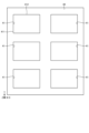
- FIG. 10 is a top view showing the housing 40 of the power semiconductor device 100 according to the first embodiment.
- the housing 40 has a plate shape and is formed with a number of openings 41 into which a portion of the heat sink integrated power module 20 is inserted.
- the housing 40 is formed with a number of openings 41 corresponding to the number of heat sink integrated power modules 20 to be mounted and the size of the heat dissipation fins 1a.
- six openings 41 are formed in order to mount six heat sink integrated power modules 20.
- the opening 41 has a rectangular shape in the in-plane direction of the housing 40.
- the shape of the opening 41 is not limited to a rectangular shape, and may be formed to match the shape of the heat sink integrated power module 20.
- the opening 41 has a size in the in-plane direction of the housing 40 that allows the entire heat dissipation fin 1a of the heat sink integrated power module 20 to be inserted, but has a size that does not allow the outer peripheral edge portion 1bp of the heat sink base 1b to be inserted.
- the opening 41 has a size and shape in the in-plane direction of the housing 40 that allows the entire heat dissipation fin 1a of the heat sink integrated power module 20 to be inserted, but does not allow the heat sink base 1b to be inserted.
- the relationship in size between the opening 41, the heat sink integrated power module 20, the heat sink base 1b, and the heat dissipation fin 1a will be described later.
- the housing 40 is made of a material having the rigidity to support the above components in order to support the weight of the heat sink integrated power module 20 and each component connected to the heat sink integrated power module 20. From the viewpoint of the product weight of the power semiconductor device 100, it is preferable that the housing 40 is as thin and lightweight as possible while still having the rigidity to support the above components.
- plated steel sheet is a preferable material for the housing 40 because it can achieve the rigidity to support the above components, as well as thinness and weight reduction. It is also possible to use materials other than plated steel sheet for the housing 40.
- the heat dissipation fins 1a of the heat sink 1 of the heat sink-integrated power module 20 are inserted into the multiple openings 41 from the outside of the holding portion 60.
- the housing 40 With the heat dissipation fins 1a stored inside the holding portion 60, the housing 40 has the outer peripheral edge portion 1bp of the heat sink base 1b placed on the adjacent region 413 adjacent to the openings 41.
- the housing 40 is supported by the ends of the two side portions 32, which are the free ends of the U-shape of the outer frame 30, and forms one side of the holding portion 60.
- the housing 40 holds the heatsink base 1b in the adjacent region 413, thereby holding the heatsink integrated power module 20. That is, the multiple heat dissipation fins 1a of the multiple heatsink integrated power modules 20 are inserted into the holding portion 60 from the opening 41, and the outer peripheral edge portion 1bp of the heatsink base 1b is supported on the adjacent region 413 adjacent to the opening 41 in the housing 40 that constitutes one surface of the holding portion 60 in the in-plane direction of the heatsink base 1b.
- the holding section 60 which is constituted by the outer frame 30 and the housing 40 having the above-mentioned configuration, has a box shape with an air inlet and an air outlet facing each other, and multiple openings 41 formed in the housing 40 that constitutes one side connecting the air inlet and the air outlet.
- the structural support portion 50 is provided inside the holding portion 60, and supports the housing 40 and the heat sink-integrated power module 20 mounted on the housing 40 by receiving a load from the housing 40 constituting one surface of the holding portion 60 toward the inside of the holding portion 60.
- the structural support portion 50 is disposed at a position corresponding to the space between the heat sink bases 1b of the heat sink-integrated power modules 20 adjacent to each other in the width direction of the holding portion 60.
- the width direction of the holding portion 60 is a direction perpendicular to the direction from the inlet of the holding portion 60 toward the outlet of the holding portion 60, and is a left-right direction.
- the direction from the inlet of the holding portion 60 toward the outlet of the holding portion 60 corresponds to the Y direction.
- the structural support portion 50 extends continuously in the direction from the inlet to the outlet in the region from the inlet of the holding portion 60 to the outlet of the holding portion 60.
- the structural support portion 50 is fixed to the outer frame 30, and the upper surface is in contact with the housing 40.
- the structural support portion 50 is rod-shaped with a rectangular cross section perpendicular to the longitudinal direction. The shape of the structural support part 50 is not limited as long as it can perform its function.
- Figures 11 to 18 are diagrams that show an example of the steps of the method for manufacturing the power semiconductor device 100 according to the first embodiment.
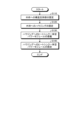
- Figure 19 is a flowchart showing the steps of the method for manufacturing the power semiconductor device 100 according to the first embodiment.
- FIG. 11 is a first top view that shows a schematic example of an exemplary procedure for the manufacturing method of the power semiconductor device 100 according to the first embodiment.
- FIG. 12 is a first cross-sectional view that shows a schematic example of an exemplary procedure for the manufacturing method of the power semiconductor device 100 according to the first embodiment.
- FIG. 12 is a cross-sectional view taken along line XII-XII in FIG. 11.
- the structural support part 50 is attached and fixed to the inner surface 31a of the bottom surface part 31 of the outer frame 30.
- the structural support part 50 is attached to the center part in the left-right direction of the inner surface 31a of the bottom surface part 31 with a cross section perpendicular to the longitudinal direction perpendicular to the inner surface 31a of the bottom surface part 31 of the outer frame 30 and with the longitudinal direction parallel to the two side surfaces 32 of the outer frame 30.
- An example of a method for fixing the structural support part 50 to the outer frame 30 is screw fastening.
- the method for fixing the structural support part 50 to the outer frame 30 is not limited to screw fastening.
- the structural support part 50 may be fixed to the inner surface 31a of the bottom surface part 31 of the outer frame 30 by welding.
- FIG. 13 is a second top view that shows an example of the procedure of the manufacturing method of the power semiconductor device 100 according to the first embodiment.
- FIG. 14 is a second cross-sectional view that shows an example of the procedure of the manufacturing method of the power semiconductor device 100 according to the first embodiment.
- FIG. 15 is a third cross-sectional view that shows an example of the procedure of the manufacturing method of the power semiconductor device 100 according to the first embodiment.
- FIG. 16 is a third top view that shows an example of the procedure of the manufacturing method of the power semiconductor device 100 according to the first embodiment.
- FIG. 17 is a fourth top view that shows an example of the procedure of the manufacturing method of the power semiconductor device 100 according to the first embodiment.
- FIG. 14 is a cross-sectional view taken along the line XIIII-XIIII in FIG. 13.
- FIG. 15 is a cross-sectional view taken along the line XV-XV in FIG. 13.
- the housing 40 is placed on the outer frame 30.
- the left-right end regions 415 of the housing 40 are placed on the side portions 32 of the outer frame 30.
- the left-right central region 414 of the housing 40 is placed on the structural support portion 50.
- the region between the short side 411 of the opening and the long side 416 of the housing in the left-right direction is defined as the end region 415.
- the region corresponding to the position between the short sides 411 of adjacent openings in the left-right direction is defined as the central region 414.
- the housing fixing screws 71 are screwed from above the end regions 415 of the housing 40 at both left and right ends, thereby fixing the housing 40 to the outer frame 30 at the end regions 415. Furthermore, as shown in FIG. 17, the housing fixing screws 71 may be screwed from above the central region 414 of the housing 40 at the center in the left and right direction, thereby fixing the housing 40 to the structural support part 50 at the central region 414.
- the outer frame 30 has a screw hole (not shown) formed in advance at the location where the housing fixing screw 71 is screwed.
- the position where the housing fixing screw 71 is screwed in the outer frame 30 is the position of the upper surface of the two side portions 32 of the outer frame 30.
- the housing 40 has a screw hole or a through hole (not shown) formed in advance at the location where the housing fixing screw 71 is screwed.
- the position where the housing fixing screw 71 is screwed in the housing 40 is a position corresponding to the screw hole of the outer frame 30 in the end region 415.
- the structural support portion 50 has a screw hole (not shown) formed in advance at the location where the housing fixing screw 71 is screwed.
- the position where the housing fixing screw 71 is screwed in the structural support portion 50 is a position corresponding to the screw hole or through hole of the central region 414 of the housing 40 on the upper surface of the structural support portion 50 fixed to the outer frame 30.
- the housing 40 is fixed to the outer frame 30 by screwing at the end regions 415, and the housing 40 is fixed to the structural support portion 50 by screwing at the central region 414, so that the housing 40 is more firmly fixed to the other components in the holding portion 60, and the vibration resistance of the holding portion 60 and the power semiconductor device 100 is improved.
- step S130 the heat sink integrated power module 20 is mounted on the housing 40. Specifically, the heat dissipation fins 1a of the heat sink integrated power module 20 are inserted from above the opening 41 of the housing 40, and the heat sink integrated power module 20 is mounted on the housing 40.
- the heat sink integrated power module 20 is placed in the adjacent region 413 adjacent to the opening 41 with the heat dissipation fins 1a housed inside the holding portion 60, with the outer peripheral edge 1bp of the heat sink base 1b being placed.
- the heat sink base 1b is supported in the adjacent region 413 of the housing 40, and the heat sink integrated power module 20 is held in the housing 40.
- the heat sink integrated power module 20 is mounted in the housing 40 such that the center position of the opening 41 of the housing 40 and the center position of the heat sink base 1b are the same in the in-plane direction of the housing 40.
- the heat sink integrated power module 20 is mounted in the housing 40 such that the depth direction of the multiple heat dissipation fins 1a in the heat sink 1 is parallel to the short side 411 of the opening, and the arrangement direction of the multiple heat dissipation fins 1a in the heat sink 1 is parallel to the long side 412 of the opening.
- step S140 the heat sink integrated power module 20 is fixed to the housing 40 by screws.
- Figure 18 is a fifth top view that shows a schematic example of a procedure for the manufacturing method of the power semiconductor device 100 according to the first embodiment.
- the power module fixing screws 72 are screwed from above the heatsink base 1b, whereby the heatsink base 1b is screwed and fixed to the housing 40 in the peripheral areas of the corners.
- the heatsink-integrated power module 20 is screwed and fixed to the housing 40 in the peripheral areas of the corners of the heatsink base 1b.
- the housing 40 has screw holes (not shown) formed in advance at the locations where the power module fixing screws 72 are screwed.
- the positions where the power module fixing screws 72 are screwed in the housing 40 are on the opening 41 side in the end region 415 and on the opening 41 side in the central region 414.
- the heat sink base 1b has screw holes (not shown) or through holes (not shown) formed in advance at the locations where the power module fixing screws 72 are screwed.
- the positions where the power module fixing screws 72 are screwed in the heat sink base 1b correspond to the screw holes in the end region 415 of the housing 40.
- FIG. 20 is a first schematic diagram illustrating an example of the size relationship between the opening 41 of the housing 40 and the heat sink base 1b of the heat sink integrated power module 20 in the power semiconductor device 100 according to the first embodiment.
- the position of the heat sink base 1b of the heat sink integrated power module 20 mounted on the housing 40 is indicated by a dashed line in a top view of the housing 40.
- the conditions shown in the following formulas (1) to (4) are satisfied in the in-plane direction of the housing 40 as shown in FIG. 20.
- the opening 41 in the following formulas (1) to (4) is the opening 41 of the housing 40.
- Length of the first short side 411a of the opening ⁇ length of the first short side 1bs1 of the heat sink base (1) Length of the second short side 411b of the opening ⁇ length of the second short side 1bs2 of the heat sink base (2) Length of the first long side 412a of the opening ⁇ length of the first long side 1bl1 of the heat sink base (3) Length of the second long side 412b of the opening ⁇ length of the second long side 1bl2 of the heat sink base (4)
- FIG. 21 is a second schematic diagram illustrating an example of the size relationship between the opening 41 of the housing 40 and the heat sink base 1b of the heat sink integrated power module 20 in the power semiconductor device 100 according to the first embodiment.
- the position of the heat sink base 1b of the heat sink integrated power module 20 mounted on the housing 40 is indicated by a dashed line in a top view of the housing 40.
- the heat sink integrated power module 20 and the housing 40 can be fixed by screwing the heat sink base 1b and the housing 40 together.
- Length of the first long side 412a of the opening ⁇ length of the first long side 1bl1 of the heat sink base (5)
- Length of the second long side 412b of the opening ⁇ length of the second long side 1bl2 of the heat sink base (6)
- the power module fixing screws 72 can be screwed in two areas between the first short side 411a of the opening and the first short side 1bs1 of the heat sink base, and two areas between the second short side 411b of the opening and the second short side 1bs2 of the heat sink base, in the peripheral areas of the four corners of the heat sink base 1b.
- FIG. 22 is a third schematic diagram illustrating an example of the size relationship between the opening 41 of the housing 40 and the heat sink base 1b of the heat sink integrated power module 20 in the power semiconductor device 100 according to the first embodiment.
- the position of the heat sink base 1b of the heat sink integrated power module 20 mounted on the housing 40 is indicated by a dashed line in the top view of the housing 40.
- the heat sink integrated power module 20 and the housing 40 can be fixed by screwing the heat sink base 1b and the housing 40 together.
- the power module fixing screws 72 can be screwed in two areas between the corners of the heat sink base 1b and the corners of the opening 41 in the peripheral areas of the three corners of the heat sink base 1b, and in one area between the second short side 411b of the opening and the second short side 1bs2 of the heat sink base.
- the vibration resistance of the power semiconductor device 100 after multiple components are assembled is best in the following order: screw fastening structure example shown in FIG. 22 ⁇ screw fastening structure example shown in FIG. 21 ⁇ screw fastening structure example shown in FIG. 20.
- the heat dissipation fins 1a of the heat sink-integrated power module 20 are inserted inside the housing 40, so in the depth direction, i.e., in the air inflow direction, the condition shown in the following formula (9) is satisfied.
- the condition shown in the following formula (10) is satisfied in the left-right direction, i.e., in the width direction of the power semiconductor device 100.
- FIG. 23 is a first cross-sectional view showing a method for manufacturing a power semiconductor device of a comparative example according to the first embodiment.
- FIG. 24 is a second cross-sectional view showing a method for manufacturing a power semiconductor device of a comparative example according to the first embodiment.
- FIGS. 23 and 24 show a cross-section at a location where the power module fixing screw 72 is screwed.
- the power semiconductor device of the comparative example has the same structure as the power semiconductor device 100, except that the retaining portion 60 does not include a structural support portion 50.
- the same components as the power semiconductor device 100 of the first embodiment are denoted by the same reference numerals as the power semiconductor device 100.
- the power module fixing screw 72 is also tightened in the direction shown by the arrow in FIG. 23 to fix the heat sink base 1b and the housing 40 using the power module fixing screw 72.
- the load of the power module fixing screw 72 is applied to the housing 40 via the heat sink base 1b.
- the retaining portion 60 does not have a structural support portion 50
- the load applied by tightening the power module fixing screw 72 may cause the housing 40 to bend as shown in FIG. 24. If the housing 40 bends, it may not be possible to fix the heat sink-integrated power module 20 to the housing 40.
- the vibration resistance of the completed product in which other components are attached to the heat sink integrated power module 20 will deteriorate, and repeated fatigue caused by vibrations applied to the power semiconductor device of the comparative example may damage the fastening parts of the screws, such as the housing fixing screw 71 and the power module fixing screw 72, and may damage the fastening parts of the screws and the components around the fastening parts of the screws.
- the structural support portion 50 is provided in the holding portion 60 in a region corresponding to the central region 414 of the housing 40. That is, in the power semiconductor device 100, the structural support portion 50 is attached and fixed to the inner surface 31a of the bottom surface portion 31 of the outer frame 30. As a result, in the power semiconductor device 100, the structural support portion 50 can bear the load when the heat sink-integrated power module 20 is fixed to the housing 40 by tightening the power module fixing screws 72 in the central region 414 of the housing 40. In addition, in a completed product in which other parts are attached to the heat sink-integrated power module 20, the structural support portion 50 can also bear the load when vibration is applied to the power semiconductor device 100. Therefore, the power semiconductor device 100 can realize a power semiconductor device with high productivity and high vibration resistance.
- FIG. 25 is a schematic diagram illustrating the flow of air inside the holding portion 60 in the power semiconductor device 100 according to the first embodiment.
- FIG. 26 is a schematic diagram illustrating the flow of air inside the holding portion 60 in a power semiconductor device of a comparative example according to the first embodiment.
- FIGS. 25 and 26 show a state seen through a part of the power semiconductor device.
- the air flow 200 blown from the ventilation system to the power semiconductor device 100 flows around the heat dissipation fins 1a of the heat sink 1 inside the holding portion 60, thereby promoting the dissipation of heat generated in the semiconductor element 5 of the power module 11 at the heat dissipation fins 1a.
- the generation of the first airflow vector 211 disturbs the airflow inside the holding portion 60, and a second airflow vector 212 that does not contribute to heat dissipation in the heat dissipation fin 1a is generated in the area corresponding to the central region 414 of the housing 40 inside the holding portion 60 and in the area corresponding to the end region 415 of the housing 40 inside the holding portion 60.
- the flow speed of the air flowing between the adjacent heat dissipation fins 1a decreases, and the heat transfer rate from the heat dissipation fins 1a between the heat dissipation fins 1a to the air around the heat dissipation fins 1a decreases, and the heat dissipation performance of the heat sink 1 decreases.
- the first airflow vector 211 and the second airflow vector 212 that do not contribute to heat dissipation in the heat dissipation fins 1a as described above are not generated. Therefore, in the power semiconductor device 100, the straightened airflow 200 flows between the adjacent heat dissipation fins 1a, so that the heat dissipation performance of the heat dissipation fins 1a can be obtained as designed.
- the above-mentioned power semiconductor device 100 uses multiple heat sink-integrated power modules 20 with high heat dissipation properties, and as compared to a power semiconductor device having a structure in which multiple power modules are fixed to one heat sink using thermally conductive grease, and a power semiconductor device having a structure in which an individualized heat sink and one power module are fixed using thermally conductive grease, a power semiconductor device with a large power capacity can be realized with good productivity. Furthermore, in the power semiconductor device 100, when replacing the heat sink-integrated power module 20, since no thermally conductive grease is used, there is no need to remove and relocate the thermally conductive grease, and the heat sink-integrated power module 20 can be replaced simply by attaching and detaching the screws, resulting in good productivity and maintainability.
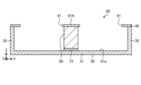
- FIG. 27 is a first cross-sectional view showing an example of a method for fixing the structural support part 50 to the outer frame 30 in the power semiconductor device 100 according to the first embodiment.
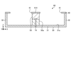
- FIG. 28 is a second cross-sectional view showing an example of a method for fixing the structural support part 50 to the outer frame 30 in the power semiconductor device 100 according to the first embodiment.
- the structural support part 50 is fixed to the inner surface 31a of the bottom surface part 31 of the outer frame 30 by a welded part 73.
- the structural support part 50 is fixed to the inner surface 31a of the bottom surface part 31 of the outer frame 30 by a structural support part fixing screw 74.
- the method of fixing the structural support part 50 to the outer frame 30 is not limited to the above example, and any method that can fix the structural support part 50 to the outer frame 30 can be applied, such as fixing the structural support part 50 to the outer frame 30 by an adhesive.
- the example shown in Figure 28 shows a cross section at the location where the structural support part fixing screw 74 is screwed.
- the structural support part 50 has a screw fixing region 50a provided in a partial region in the longitudinal direction of the structural support part 50.
- the screw fixing region 50a is an area for fixing the structural support part 50 to the inner surface 31a of the bottom part 31 of the outer frame 30 with the structural support part fixing screw 74.
- the screw fixing region 50a can be provided at any position in the longitudinal direction of the structural support part 50, provided that the structural support part 50 can be fixed to the outer frame 30 by the structural support part fixing screw 74. Furthermore, any number of screw fixing regions 50a can be provided, provided that the structural support part 50 can be fixed to the outer frame 30 by the structural support part fixing screw 74.
- the screw fixing region 50a can be provided, for example, at one location in the center of the structural support part 50 in the longitudinal direction, or can be provided, for example, at two locations on both ends of the structural support part 50 in the longitudinal direction.
- the height of the screw fixing region 50a can be any height as long as the structural support part 50 can be fixed to the outer frame 30 by the structural support part fixing screws 74.
- the height of the screw fixing region 50a is half the height of the area of the structural support part 50 other than the screw fixing region 50a.
- the height of the screw fixing region 50a may also be the same height as the area of the structural support part 50 other than the screw fixing region 50a.
- the central region 414 of the housing 40 is not provided in the area corresponding to the upper part of the screw fixing region 50a.
- FIG. 29 is a third cross-sectional view showing an example of a method for fixing the structural support part 50 to the outer frame 30 in the power semiconductor device 100 according to the first embodiment.
- FIG. 30 is a fourth cross-sectional view showing an example of a method for fixing the structural support part 50 to the outer frame 30 in the power semiconductor device 100 according to the first embodiment.
- FIG. 29 corresponds to FIG. 27, and the structural support part 50 is fixed to the inner surface 31a of the bottom part 31 in the outer frame 30 by a welding part 73.
- FIG. 30 corresponds to FIG. 28, and the structural support part 50 is fixed to the inner surface 31a of the bottom part 31 in the outer frame 30 by a structural support part fixing screw 74.
- the deformation of the housing 40 when the power module fixing screw 72 is tightened can be reduced.
- the power semiconductor device 100 can suppress the bending of the housing 40 when the power module fixing screw 72 is tightened, reducing the occurrence rate of defects when fixing the heat sink integrated power module 20 to the housing 40 and improving productivity.
- the vibration resistance of a completed product in which other parts are attached to the heat sink integrated power module 20 the deformation of the housing 40 when vibration is applied to the power semiconductor device 100 can be suppressed or the deformation of the housing 40 can be controlled. Therefore, the vibration resistance of the product is improved.
- the power semiconductor device 100 can achieve the same effect as when there is no gap 80 between the central region 414 of the housing 40 and the upper surface of the structural support portion 50.
- Figure 31 is a first cross-sectional view showing an example of a method for fixing the structural support part 50 to the housing 40 in the power semiconductor device 100 according to the first embodiment.
- Figure 32 is a second cross-sectional view showing an example of a method for fixing the structural support part 50 to the housing 40 in the power semiconductor device 100 according to the first embodiment.
- the structural support part 50 has an upper surface fixed to the central region 414 of the housing 40 by a welded part 75, and a lower surface in contact with the inner surface 31a of the bottom part 31 of the outer frame 30.
- the structural support part 50 is fixed to the central region 414 of the housing 40 by a structural support part fixing screw 76, and a lower surface in contact with the inner surface 31a of the bottom part 31 of the outer frame 30.
- the method of fixing the structural support part 50 to the housing 40 is not limited to the above example, and any method that can fix the structural support part 50 to the housing 40 can be applied, such as fixing the structural support part 50 to the housing 40 with an adhesive.
- FIG. 33 is a flowchart showing the steps of another method for manufacturing the power semiconductor device 100 according to the first embodiment. Here, a method for manufacturing the power semiconductor device 100 in the case where the structural support portion 50 is fixed to the housing 40 is described.
- step S210 the structural support part 50 is attached and fixed to the housing 40.
- the structural support part 50 is fixed to the housing 40 by the welded part 75 or the structural support part fixing screw 76 as described above.
- step S220 the housing 40 is fixed to the outer frame 30 using the housing fixing screws 71 in the same manner as in step S120.
- step S230 the heat sink integrated power module 20 is mounted in the housing 40 in the same manner as in step S130.
- step S240 the heat sink integrated power module 20 is screwed and fixed to the housing 40 in the same manner as in step S140.
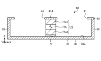
- FIG. 34 is a first cross-sectional view showing the structure of the power semiconductor device 100 when a structural support part with elastic function 77 is applied to the power semiconductor device 100 according to the first embodiment.
- FIG. 35 is a second cross-sectional view showing the structure of the power semiconductor device 100 when a structural support part with elastic function 77 is applied to the power semiconductor device 100 according to the first embodiment.
- the elastic support part 77 is a structural support part having elasticity. Therefore, by using the elastic support part 77 to fix the housing 40 and the structural support part 50, even if there is dimensional variation or assembly tolerance in the manufacture of each part constituting the holding part 60, the elasticity of the elastic support part 77 absorbs the dimensional variation and assembly tolerance in the manufacture of each part. This makes it possible for the power semiconductor device 100 to fix the housing 40 and the structural support part 50 in a state where the housing 40 and the structural support part 50 are in secure contact with each other. By using the elastic support part 77, the power semiconductor device 100 can further stably improve the vibration resistance.
- the elastic structural support part 77 is structured such that the structural support part is divided into two divided parts, a first divided structural support part 77a1 and a second divided structural support part 77a2, and a coil spring 77b is inserted between the first divided structural support part 77a1 and the second divided structural support part 77a2.
- the first divided structural support part 77a1 is disposed on the central region 414 side of the housing 40 in the height direction.
- the second divided structural support part 77a2 is disposed on the bottom surface part 31 side of the outer frame 30 in the height direction.
- the elastic function-equipped structural support part 77 has a second divided structural support part 77a2 arranged on the bottom surface part 31 side of the outer frame 30 in the height direction, which is fixed to the inner surface 31a of the bottom surface part 31 of the outer frame 30 by a welded part 73.
- the elastic function-equipped structural support part 77 has a second divided structural support part 77a2 arranged on the bottom surface part 31 side of the outer frame 30 in the height direction, which is fixed to the inner surface 31a of the bottom surface part 31 of the outer frame 30 by a structural support part fixing screw 74.
- FIG. 35 shows a cross section at the location where the structural support part fixing screw 74 is screwed.
- the second divided structural support part 77a2 has a screw fixing region 77c provided in a partial region in the longitudinal direction of the second divided structural support part 77a2.
- the longitudinal direction of the second divided structural support part 77a2 can be said to be the longitudinal direction of the elastic function-equipped structural support part 77.
- the screw fixing region 77c is a region for fixing the second divided structural support part 77a2 to the inner surface 31a of the bottom surface part 31 of the outer frame 30 with the structural support part fixing screw 74.
- the coil spring 77b and the first divided structural support part 77a1 are not positioned above the screw fixing region 77c.
- the screw fixing region 77c can be provided at any position in the longitudinal direction of the second divided structure support part 77a2, provided that the second divided structure support part 77a2 can be fixed to the outer frame 30 by the structural support part fixing screw 74. Furthermore, any number of screw fixing regions 77c can be provided, provided that the second divided structure support part 77a2 can be fixed to the outer frame 30 by the structural support part fixing screw 74.
- the screw fixing region 77c can be provided, for example, at one location in the center of the second divided structure support part 77a2 in the longitudinal direction, or can be provided, for example, at two locations on both ends of the second divided structure support part 77a2 in the longitudinal direction.
- the height of the screw fixing region 77c can be any height as long as the second divided structure support part 77a2 can be fixed to the outer frame 30 by the structure support part fixing screw 74.
- the height of the screw fixing region 77c is 1/3 the height of the area other than the screw fixing region 77c in the second divided structure support part 77a2.
- the height of the screw fixing region 77c may also be the same height as the height of the area other than the screw fixing region 77c in the second divided structure support part 77a2.
- the structure of the elastic structural support portion 77 is not limited to the above example.
- the power semiconductor device 100 can achieve the same effect as above even if it has a configuration in which a sponge with elastic properties is sandwiched between at least one of the inner surface 31a of the bottom portion 31 of the outer frame 30 and the structural support portion 50, and between the central region 414 of the housing 40 and the structural support portion 50.
- Figure 36 is a first cross-sectional view illustrating the positional relationship between the structural support part 50, the heat sink base 1b of the heat sink integrated power module, and the housing 40 in the power semiconductor device 100 according to the first embodiment.
- the structural support portion width dimension 50L which is the width dimension of the structural support portion 50, is larger than the dimension of the gap 81 between the heat sink bases 1b of adjacent heat sink-integrated power modules 20 in the left-right direction.
- the structural support portion width dimension 50L is set to a dimension that allows the power module fixing screw 72 to be fastened in the central region 414 of the housing 40.
- the heat sink bases 1b of the heat sink-integrated power modules 20 adjacent in the left-right direction are mounted on the housing 40.
- the heat sink bases 1b and the housing 40 are fixed by the power module fixing screws 72 in the end regions 415 of the housing 40.
- the power module fixing screws 72 are tightened from above the central region 414 of the housing 40, thereby fixing the heat sink bases 1b, the housing 40, and the structural support portion 50 by the power module fixing screws 72.
- the heat sink integrated power module 29 is firmly fixed to the holding portion 60, resulting in a power semiconductor device 100 with higher vibration resistance.
- the cross-sectional area of the air passage along the XZ plane inside the holding portion 60 is reduced, the flow rate of the air flowing between adjacent heat dissipation fins 1a is increased, the heat transfer rate from between the heat dissipation fins 1a to the air around the heat dissipation fins 1a is increased, and the heat dissipation performance of the heat sink 1 is optimized.
- FIG. 37 is a second cross-sectional view illustrating the relationship between the structural support part 50, the heat sink base 1b of the heat sink integrated power module, and the housing 40 in the power semiconductor device 100 according to the first embodiment.
- FIG. 38 is a third cross-sectional view illustrating the relationship between the structural support part 50, the heat sink base 1b of the heat sink integrated power module, and the housing 40 in the power semiconductor device 100 according to the first embodiment.
- the structural support width dimension 50L is larger than the dimension of the gap 81 between the heat sink bases 1b of the heat sink-integrated power modules 20 adjacent in the left-right direction.
- the structural support width dimension 50L is smaller than the dimension of the gap 81 between the heat sink bases 1b of the heat sink-integrated power modules 20 adjacent in the left-right direction.
- the dimension of the gap 81 is set to a dimension that allows the housing fixing screw 71 to be tightened in the central region 414 of the housing 40.
- the housing 40 and the structural support portion 50 are fixed by the housing fixing screw 71, which is screwed from above the central region 414 of the housing 40.
- a power semiconductor device 100 structure having high vibration resistance is obtained while ensuring the fixing strength of the holding portion 60.
- the vibration resistance of the power semiconductor device 100 is improved in the following order: structure shown in FIG. 36 > structure shown in FIG. 37 > structure shown in FIG. 38.
- the structure shown in FIG. 36 can reduce the number of screws used compared to the structures shown in FIG. 37 and FIG. 38, improving the productivity of the power semiconductor device 100 and reducing the manufacturing costs of the power semiconductor device 100.
- FIG. 39 is a first top view illustrating the shape and arrangement of the structural support part 50 in the power semiconductor device 100 according to the first embodiment.
- a part of the configuration of the power semiconductor device 100 is omitted.
- the longitudinal direction of the structural support part 50 is parallel to the depth direction of the power semiconductor device 100, that is, the traveling direction of the air flow 200 inside the holding part 60, in the in-plane direction of the bottom part 31 of the outer frame 30 and the in-plane direction of the housing 40.
- the structural support part 50 extends continuously from the end part 33 on the front side of the outer frame 30 to the end part 34 on the back side of the outer frame 30.
- the structural support part 50 extends continuously in the region from the wind inlet to the wind outlet in the holding part 60 in the direction from the inlet to the outlet. Note that the shape and arrangement of the structural support part 50 are not limited to the structure shown in FIG. 39.
- FIG. 40 is a second top view illustrating the shape and arrangement of the structural support portion 50 in the power semiconductor device 100 according to the first embodiment.
- a portion of the configuration of the power semiconductor device 100 is omitted.
- the structural support portion 50 is partially arranged in a part of the region on the upwind side of the traveling direction of the air flow 200 flowing inside the holding portion 60, including adjacent corners of each heat sink base 1b of two heat sink-integrated power modules 20 adjacent in the left-right direction, in the in-plane direction of the bottom surface portion 31 of the outer frame 30 and in the in-plane direction of the housing 40.
- the structural support portion 50 is partially arranged in a part of the region on the downwind side of the traveling direction of the air flow 200 flowing inside the holding portion 60, including adjacent corners of each heat sink base 1b of two heat sink-integrated power modules 20 adjacent in the left-right direction, in the in-plane direction of the bottom surface portion 31 of the outer frame 30 and in the in-plane direction of the housing 40. That is, the structural support parts 50 are arranged discontinuously in the direction from the inlet to the outlet in the region from the air inlet to the air outlet in the holding part 60.
- FIG. 41 is a third top view illustrating the shape and arrangement of the structural support portion 50 in the power semiconductor device 100 according to the first embodiment.
- a portion of the configuration of the power semiconductor device 100 is omitted.
- the structural support portion 50 is partially arranged in a part of the region on the upwind side of the traveling direction of the air flow 200 flowing inside the holding portion 60, including adjacent corners of the heat sink bases 1b of the two heat sink integrated power modules 20 adjacent to each other in the left-right direction in the in-plane direction of the bottom surface portion 31 of the outer frame 30 and in the in-plane direction of the housing 40.
- the structural support portion 50 is partially arranged in a part of the region on the downwind side of the traveling direction of the air flow 200 flowing inside the holding portion 60, including adjacent corners of the heat sink bases 1b of the two heat sink integrated power modules 20 adjacent to each other in the left-right direction in the in-plane direction of the bottom surface portion 31 of the outer frame 30 and in the in-plane direction of the housing 40.
- the structural support parts 50 are partially arranged in a part of the area including adjacent corners of the heat sink bases 1b of the four adjacent heat sink-integrated power modules 20 in the in-plane direction of the bottom surface part 31 of the outer frame 30 and in the in-plane direction of the housing 40. That is, the structural support parts 50 are discontinuously arranged in the area from the air inlet to the air outlet of the holding part 60 in the direction from the inlet to the outlet.
- FIG. 42 is a fourth top view illustrating the shape and arrangement of the structural support portion 50 in the power semiconductor device 100 according to the first embodiment.
- FIG. 42 some of the configuration of the power semiconductor device 100 is omitted.
- the structural support portion 50 is partially arranged in a part of an area including a central area in the depth direction of each heat sink base 1b of two heat sink-integrated power modules 20 adjacent in the left-right direction in the in-plane direction of the bottom surface portion 31 of the outer frame 30 and in the in-plane direction of the housing 40.
- the structures shown in Figures 39 to 42 provide a power semiconductor device 100 with high vibration resistance, as described above.
- the power semiconductor device 100 by arranging the structural support part 50 on the upwind side of the air flow 200 in the holding part 60, the air flow 200 blown from the ventilation system can be straightened and flowed between adjacent heat dissipation fins 1a. This allows the power semiconductor device 100 to obtain the heat dissipation performance as designed.
- the vibration resistance effect of the power semiconductor device 100 with the above structure is improved in the following order: structure shown in Figure 39 > structure shown in Figure 40 > structure shown in Figure 41 > structure shown in Figure 42.
- the structural support portion 50 is disposed on the bottom surface portion 31 of the outer frame 30 of the holding portion 60 so as to receive the load of the multiple heat sink integrated power modules 20 and the housing 40 on which the multiple heat sink integrated power modules 20 are mounted. Therefore, in the power semiconductor device 100, it is possible to suppress the bending of the housing 40 that occurs when the multiple heat sink integrated power modules 20 are fixed to the housing 40.
- the power semiconductor device 100 it is possible to suppress or prevent a decrease in the heat dissipation performance of the heat sink 1 caused by a gap that occurs between the heat sink 1 and the housing 49 when the housing 40 is bent, and the heat dissipation performance and vibration resistance of the heat generated in the power module 11 are improved.
- the structural support section 50 is disposed in a region on the bottom surface section 31 of the outer frame 30 that corresponds to the central region 414 of the housing 40. This allows the structural support section 50 to evenly bear the load of two heat sink-integrated power modules 20 adjacent to each other in the left-right direction, and further suppresses deflection of the housing 40 that occurs when multiple heat sink-integrated power modules 20 are fixed to the housing 40.
- the structural support part 50 is positioned on the upwind side inside the holding part 60, so that the structural support part 50 forms an air path to rectify the airflow 200 flowing into the holding part 60, and the rectified air can be made to flow into the heat sink 1, improving the dissipation of heat generated in the power module 11.
- the configuration of the power semiconductor device 100 makes it possible to apply multiple heat sink-integrated power modules 20 with high heat dissipation performance to high-capacity power systems in which multiple power modules are used while maintaining high heat dissipation and high vibration resistance.
- the power semiconductor device 100 has the effect of suppressing bending of the housing to which the multiple power modules and heat sinks are attached.
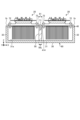
- Embodiment 2. 43 is a cross-sectional view showing a configuration of a power semiconductor device 101 according to the second embodiment.
- the power semiconductor device 101 according to the second embodiment is different from the power semiconductor device 100 according to the first embodiment in that the power semiconductor device 101 according to the second embodiment includes a structural support portion 51 instead of the structural support portion 50.
- the structural support portion 51 has a through hole 51a penetrating the structural support portion 51 in the depth direction. That is, the structural support portion 51 has a through hole 51a penetrating the structural support portion 51 in the direction from the inlet to the outlet of the holding portion 60.
- the structural support portion 51 has the through hole 51a, so that the surface area of the structural support portion 51 is increased, and therefore the heat dissipation performance of the structural support portion 51 for heat generated in the semiconductor element 5 of the power module 11 is improved.
- FIG. 44 is a cross-sectional view showing the configuration of a power semiconductor device 102 according to the second embodiment.
- the power semiconductor device 102 according to the second embodiment differs from the power semiconductor device 100 according to the first embodiment in that it has a structural support part 52 instead of the structural support part 50.
- the structural support part 52 has irregularities 52a on the surface of the structural support part 52.
- the structural support part 52 has irregularities 52a, which increases the surface area of the structural support part 52, thereby improving the heat dissipation performance of the structural support part 52 for heat generated in the semiconductor element 5 of the power module 11.
- Fig. 45 is a cross-sectional view showing the configuration of a heat sink integrated power module 21 according to the third embodiment.
- Fig. 46 is a cross-sectional view showing the configuration of a power semiconductor device 103 according to the third embodiment.
- the above-mentioned power semiconductor device 100 uses a heat sink-integrated power module 20 in which one heat sink 1 is provided for one power module 11, improving handling when assembling the power semiconductor device 100 and ease of attaching and detaching parts during maintenance.
- one heat sink 1 is individualized for one power module 11, so the number of screws required to fasten the heat sink-integrated power module 20 to the housing 40 increases compared to when multiple power modules are mounted on one heat sink, which may reduce productivity.
- a convex portion 22 is provided at the end of the heat sink base 1b in the in-plane direction of the heat sink base 1b.
- a first convex portion 22a which is a convex portion 22 is provided at the end of the heatsink base 1b in the in-plane direction of the heatsink base 1b.
- the first convex portion 22a is provided at the end of the heatsink base 1b on the side of the other power semiconductor device 103 adjacent in the left-right direction.
- the first convex portion 22a is also provided at the upper portion at the end of the heatsink base 1b.
- a second convex portion 22b which is a convex portion 22 is provided at the end of the heatsink base 1b in the in-plane direction of the heatsink base 1b.
- the second convex portion 22b is provided at the end of the heatsink base 1b on the side of the other power semiconductor device 103 adjacent in the left-right direction.
- the second convex portion 22b is also provided at the lower part of the end of the heatsink base 1b.
- the first heat sink integrated power module 21a and the second heat sink integrated power module 21b are mounted on the housing 40 with the first convex portion 22a of the first heat sink integrated power module 21a and the second convex portion 22b of the second heat sink integrated power module 21b overlapping each other. Then, the first convex portion 22a, the second convex portion 22b, and the structural support portion 50 are fixed by tightening the power module fixing screws 72 to the overlapping first convex portion 22a and second convex portion 22b, the central region 414 of the housing 40, and the structural support portion 50. That is, the first convex portion 22a, the second convex portion 22b, the central region 414 of the housing 40, and the structural support portion 50 are screwed and fixed in an overlapping state.
- the number of screws required to fasten the heat sink-integrated power module 20 to the housing 40 can be reduced, improving productivity.
- the area in the central region 414 of the housing 40 in which the first heat sink integrated power module 21a, the second heat sink integrated power module 21b, and the structural support portion 50 are fixed can be narrowed in the left-right direction. This makes it possible to increase the number of heat dissipation fins 1a provided on the heat sink base 1b. As a result, in the power semiconductor device 103, the heat dissipation performance of the heat sink 1 for dissipating heat generated in the semiconductor element 5 of the power module 11 is improved.
- the heat sink is a first modified heat sink, the second modified heat sink, the third modified heat sink, the fourth modified heat sink, the fifth modified heat sink, the fifth modified heat sink, the sixth modified heat sink, the fifth modified heat sink, the sixth modified heat sink, the seventh modified heat sink, the eighth ...
Landscapes
- Cooling Or The Like Of Semiconductors Or Solid State Devices (AREA)
- Cooling Or The Like Of Electrical Apparatus (AREA)
Priority Applications (4)
| Application Number | Priority Date | Filing Date | Title |
|---|---|---|---|
| US18/880,361 US20250167073A1 (en) | 2022-10-13 | 2022-10-13 | Power semiconductor device and method of manufacturing power semiconductor device |
| JP2023509445A JP7258269B1 (ja) | 2022-10-13 | 2022-10-13 | 電力半導体装置および電力半導体装置の製造方法 |
| CN202280097747.6A CN119604980B (zh) | 2022-10-13 | 2022-10-13 | 电力半导体装置及电力半导体装置的制造方法 |
| PCT/JP2022/038210 WO2024079846A1 (ja) | 2022-10-13 | 2022-10-13 | 電力半導体装置および電力半導体装置の製造方法 |
Applications Claiming Priority (1)
| Application Number | Priority Date | Filing Date | Title |
|---|---|---|---|
| PCT/JP2022/038210 WO2024079846A1 (ja) | 2022-10-13 | 2022-10-13 | 電力半導体装置および電力半導体装置の製造方法 |
Publications (1)
| Publication Number | Publication Date |
|---|---|
| WO2024079846A1 true WO2024079846A1 (ja) | 2024-04-18 |
Family
ID=85980405
Family Applications (1)
| Application Number | Title | Priority Date | Filing Date |
|---|---|---|---|
| PCT/JP2022/038210 Ceased WO2024079846A1 (ja) | 2022-10-13 | 2022-10-13 | 電力半導体装置および電力半導体装置の製造方法 |
Country Status (4)
| Country | Link |
|---|---|
| US (1) | US20250167073A1 (https=) |
| JP (1) | JP7258269B1 (https=) |
| CN (1) | CN119604980B (https=) |
| WO (1) | WO2024079846A1 (https=) |
Families Citing this family (2)
| Publication number | Priority date | Publication date | Assignee | Title |
|---|---|---|---|---|
| CN121400138A (zh) * | 2023-07-27 | 2026-01-23 | 三菱电机株式会社 | 电力半导体装置 |
| WO2025243727A1 (ja) * | 2024-05-22 | 2025-11-27 | 三菱電機株式会社 | 電力半導体装置、及び、電力変換装置 |
Citations (3)
| Publication number | Priority date | Publication date | Assignee | Title |
|---|---|---|---|---|
| WO2012029165A1 (ja) * | 2010-09-02 | 2012-03-08 | トヨタ自動車株式会社 | 半導体モジュール |
| JP2012199596A (ja) * | 2012-07-25 | 2012-10-18 | Mitsubishi Electric Corp | 半導体モジュール |
| JP2014220334A (ja) * | 2013-05-07 | 2014-11-20 | 株式会社安川電機 | 電力変換装置 |
Family Cites Families (20)
| Publication number | Priority date | Publication date | Assignee | Title |
|---|---|---|---|---|
| EP0835524A1 (de) * | 1996-01-04 | 1998-04-15 | Daimler-Benz Aktiengesellschaft | Kühlkörper mit zapfen |
| JP2001035981A (ja) * | 1999-07-16 | 2001-02-09 | Toshiba Corp | 半導体素子用冷却器及びこれを用いた電力変換装置 |
| US6414867B2 (en) * | 2000-02-16 | 2002-07-02 | Hitachi, Ltd. | Power inverter |
| US8125781B2 (en) * | 2004-11-11 | 2012-02-28 | Denso Corporation | Semiconductor device |
| WO2007032056A1 (ja) * | 2005-09-13 | 2007-03-22 | Mitsubishi Denki Kabushiki Kaisha | ヒートシンク |
| TWM300577U (en) * | 2006-05-25 | 2006-11-11 | Cooler Master Co Ltd | Perforation spreading jig of heat-dissipating fin |
| JP5084527B2 (ja) * | 2008-01-23 | 2012-11-28 | 三菱電機株式会社 | ヒートシンクおよび電気機器 |
| JP5314933B2 (ja) * | 2008-06-02 | 2013-10-16 | 本田技研工業株式会社 | 電力変換装置 |
| JP5089662B2 (ja) * | 2009-08-04 | 2012-12-05 | 三菱電機株式会社 | 半導体モジュール |
| EP2465138B1 (en) * | 2009-08-10 | 2016-11-23 | Fuji Electric Co., Ltd. | Semiconductor module and cooling unit |
| JP2011155207A (ja) * | 2010-01-28 | 2011-08-11 | Aisin Aw Co Ltd | インバータモジュールの製造方法及びインバータモジュール |
| CN101975376B (zh) * | 2010-10-08 | 2012-07-11 | 深圳市华星光电技术有限公司 | 背光模块的发光源散热构造 |
| JPWO2012157247A1 (ja) * | 2011-05-16 | 2014-07-31 | 富士電機株式会社 | 半導体モジュール用冷却器 |
| US20130027885A1 (en) * | 2011-07-25 | 2013-01-31 | International Business Machines Corporation | Heat spreader for multi-chip modules |
| JP5716610B2 (ja) * | 2011-08-30 | 2015-05-13 | 株式会社デンソー | 電力変換装置 |
| JP2013074721A (ja) * | 2011-09-28 | 2013-04-22 | Denso Corp | 電力変換装置 |
| JP5901343B2 (ja) * | 2012-02-24 | 2016-04-06 | 三菱電機株式会社 | 冷却器及び冷却装置 |
| JP6227970B2 (ja) * | 2013-10-16 | 2017-11-08 | 本田技研工業株式会社 | 半導体装置 |
| JP6318857B2 (ja) * | 2014-05-27 | 2018-05-09 | 富士通株式会社 | ヒートシンク及び基板ユニット |
| JP6789335B2 (ja) * | 2019-03-05 | 2020-11-25 | 三菱電機株式会社 | ヒートシンク及びこれを備えた半導体モジュール |
-
2022
- 2022-10-13 CN CN202280097747.6A patent/CN119604980B/zh active Active
- 2022-10-13 WO PCT/JP2022/038210 patent/WO2024079846A1/ja not_active Ceased
- 2022-10-13 US US18/880,361 patent/US20250167073A1/en active Pending
- 2022-10-13 JP JP2023509445A patent/JP7258269B1/ja active Active
Patent Citations (3)
| Publication number | Priority date | Publication date | Assignee | Title |
|---|---|---|---|---|
| WO2012029165A1 (ja) * | 2010-09-02 | 2012-03-08 | トヨタ自動車株式会社 | 半導体モジュール |
| JP2012199596A (ja) * | 2012-07-25 | 2012-10-18 | Mitsubishi Electric Corp | 半導体モジュール |
| JP2014220334A (ja) * | 2013-05-07 | 2014-11-20 | 株式会社安川電機 | 電力変換装置 |
Also Published As
| Publication number | Publication date |
|---|---|
| CN119604980B (zh) | 2026-01-16 |
| CN119604980A (zh) | 2025-03-11 |
| JP7258269B1 (ja) | 2023-04-14 |
| US20250167073A1 (en) | 2025-05-22 |
| JPWO2024079846A1 (https=) | 2024-04-18 |
Similar Documents
| Publication | Publication Date | Title |
|---|---|---|
| JP6743916B2 (ja) | 半導体装置及び半導体装置の製造方法 | |
| CN101443904B (zh) | 功率模块用基体 | |
| JP5432085B2 (ja) | 電力半導体装置 | |
| JP5014016B2 (ja) | 半導体装置 | |
| JP7258269B1 (ja) | 電力半導体装置および電力半導体装置の製造方法 | |
| CN102473694A (zh) | 半导体模块和散热构件 | |
| JP2010161203A (ja) | 放熱装置、パワーモジュール、パワーモジュールの製造方法 | |
| JPWO2008142760A1 (ja) | 電力用半導体モジュール | |
| JP2013030649A (ja) | 半導体モジュール及びその製造方法 | |
| JP7479580B1 (ja) | 電力半導体装置 | |
| US20180337153A1 (en) | Semiconductor module, base plate of semiconductor module, and method of manufacturing semiconductor device | |
| JP4046623B2 (ja) | パワー半導体モジュールおよびその固定方法 | |
| JP2006287080A (ja) | メモリモジュール | |
| JP2018198508A (ja) | 電力半導体装置、及び電力変換装置 | |
| JP2016086134A (ja) | ヒートシンク、ヒートシンク一体型パワーモジュールおよびそれらの製造方法 | |
| JP2006140390A (ja) | パワー半導体装置 | |
| JP4723661B2 (ja) | 受熱面平行フィン型扁平状放熱構造体 | |
| WO2023067894A1 (ja) | 冷却装置及び冷却装置の製造方法 | |
| CN100459108C (zh) | 半导体器件 | |
| JP2007165426A (ja) | 半導体装置 | |
| WO2014045711A1 (ja) | 半導体モジュール | |
| JP2017162922A (ja) | 冷却チューブ | |
| JP7452184B2 (ja) | 電力変換装置 | |
| JP4556732B2 (ja) | 半導体装置及びその製造方法 | |
| JP2006210611A (ja) | 放熱フィンを備えたヒートシンク及びその製造方法。 |
Legal Events
| Date | Code | Title | Description |
|---|---|---|---|
| ENP | Entry into the national phase |
Ref document number: 2023509445 Country of ref document: JP Kind code of ref document: A |
|
| 121 | Ep: the epo has been informed by wipo that ep was designated in this application |
Ref document number: 22962065 Country of ref document: EP Kind code of ref document: A1 |
|
| WWE | Wipo information: entry into national phase |
Ref document number: 18880361 Country of ref document: US Ref document number: 202280097747.6 Country of ref document: CN |
|
| WWP | Wipo information: published in national office |
Ref document number: 202280097747.6 Country of ref document: CN |
|
| NENP | Non-entry into the national phase |
Ref country code: DE |
|
| WWP | Wipo information: published in national office |
Ref document number: 18880361 Country of ref document: US |
|
| 122 | Ep: pct application non-entry in european phase |
Ref document number: 22962065 Country of ref document: EP Kind code of ref document: A1 |