WO2024079846A1 - Power semiconductor device and method for manufacturing power semiconductor device - Google Patents
Power semiconductor device and method for manufacturing power semiconductor device Download PDFInfo
- Publication number
- WO2024079846A1 WO2024079846A1 PCT/JP2022/038210 JP2022038210W WO2024079846A1 WO 2024079846 A1 WO2024079846 A1 WO 2024079846A1 JP 2022038210 W JP2022038210 W JP 2022038210W WO 2024079846 A1 WO2024079846 A1 WO 2024079846A1
- Authority
- WO
- WIPO (PCT)
- Prior art keywords
- heat sink
- semiconductor device
- housing
- structural support
- power semiconductor
- Prior art date
Links
- 239000004065 semiconductor Substances 0.000 title claims abstract description 257
- 238000000034 method Methods 0.000 title claims description 60
- 238000004519 manufacturing process Methods 0.000 title claims description 39
- 230000017525 heat dissipation Effects 0.000 claims abstract description 92
- 230000002093 peripheral effect Effects 0.000 claims abstract description 16
- 230000000630 rising effect Effects 0.000 claims description 4
- 230000000149 penetrating effect Effects 0.000 claims description 3
- 239000000463 material Substances 0.000 description 18
- 239000011347 resin Substances 0.000 description 12
- 229920005989 resin Polymers 0.000 description 12
- 230000000052 comparative effect Effects 0.000 description 11
- 238000010586 diagram Methods 0.000 description 11
- 238000007789 sealing Methods 0.000 description 10
- 230000000694 effects Effects 0.000 description 9
- 229910052782 aluminium Inorganic materials 0.000 description 7
- XAGFODPZIPBFFR-UHFFFAOYSA-N aluminium Chemical compound [Al] XAGFODPZIPBFFR-UHFFFAOYSA-N 0.000 description 7
- 239000004020 conductor Substances 0.000 description 7
- 229910052751 metal Inorganic materials 0.000 description 7
- 239000002184 metal Substances 0.000 description 7
- 239000007769 metal material Substances 0.000 description 7
- 239000004519 grease Substances 0.000 description 6
- 229910000679 solder Inorganic materials 0.000 description 6
- 238000005452 bending Methods 0.000 description 5
- 238000007664 blowing Methods 0.000 description 5
- 230000007423 decrease Effects 0.000 description 5
- 229910000831 Steel Inorganic materials 0.000 description 4
- 238000004512 die casting Methods 0.000 description 4
- 238000001125 extrusion Methods 0.000 description 4
- 238000012545 processing Methods 0.000 description 4
- 239000010959 steel Substances 0.000 description 4
- 229910000838 Al alloy Inorganic materials 0.000 description 3
- 239000000853 adhesive Substances 0.000 description 3
- 230000001070 adhesive effect Effects 0.000 description 3
- 230000007797 corrosion Effects 0.000 description 3
- 238000005260 corrosion Methods 0.000 description 3
- 238000002788 crimping Methods 0.000 description 3
- 238000005520 cutting process Methods 0.000 description 3
- 238000005242 forging Methods 0.000 description 3
- 238000003672 processing method Methods 0.000 description 3
- 238000012546 transfer Methods 0.000 description 3
- 238000009423 ventilation Methods 0.000 description 3
- 238000003466 welding Methods 0.000 description 3
- XUIMIQQOPSSXEZ-UHFFFAOYSA-N Silicon Chemical compound [Si] XUIMIQQOPSSXEZ-UHFFFAOYSA-N 0.000 description 2
- 238000005336 cracking Methods 0.000 description 2
- 238000003825 pressing Methods 0.000 description 2
- 229910052710 silicon Inorganic materials 0.000 description 2
- 239000010703 silicon Substances 0.000 description 2
- 238000001721 transfer moulding Methods 0.000 description 2
- 239000013585 weight reducing agent Substances 0.000 description 2
- NAWXUBYGYWOOIX-SFHVURJKSA-N (2s)-2-[[4-[2-(2,4-diaminoquinazolin-6-yl)ethyl]benzoyl]amino]-4-methylidenepentanedioic acid Chemical compound C1=CC2=NC(N)=NC(N)=C2C=C1CCC1=CC=C(C(=O)N[C@@H](CC(=C)C(O)=O)C(O)=O)C=C1 NAWXUBYGYWOOIX-SFHVURJKSA-N 0.000 description 1
- RYGMFSIKBFXOCR-UHFFFAOYSA-N Copper Chemical compound [Cu] RYGMFSIKBFXOCR-UHFFFAOYSA-N 0.000 description 1
- 239000004593 Epoxy Substances 0.000 description 1
- 229910002601 GaN Inorganic materials 0.000 description 1
- JMASRVWKEDWRBT-UHFFFAOYSA-N Gallium nitride Chemical compound [Ga]#N JMASRVWKEDWRBT-UHFFFAOYSA-N 0.000 description 1
- 238000001816 cooling Methods 0.000 description 1
- 229910052802 copper Inorganic materials 0.000 description 1
- 239000010949 copper Substances 0.000 description 1
- 230000007547 defect Effects 0.000 description 1
- 239000010432 diamond Substances 0.000 description 1
- 229910003460 diamond Inorganic materials 0.000 description 1
- 238000005516 engineering process Methods 0.000 description 1
- 230000014509 gene expression Effects 0.000 description 1
- 230000012447 hatching Effects 0.000 description 1
- 238000003780 insertion Methods 0.000 description 1
- 230000037431 insertion Effects 0.000 description 1
- 238000009413 insulation Methods 0.000 description 1
- 238000012423 maintenance Methods 0.000 description 1
- 238000000465 moulding Methods 0.000 description 1
- 230000001737 promoting effect Effects 0.000 description 1
- HBMJWWWQQXIZIP-UHFFFAOYSA-N silicon carbide Chemical compound [Si+]#[C-] HBMJWWWQQXIZIP-UHFFFAOYSA-N 0.000 description 1
- 239000000758 substrate Substances 0.000 description 1
- 229920001187 thermosetting polymer Polymers 0.000 description 1
Images


Classifications
-
- H—ELECTRICITY
- H01—ELECTRIC ELEMENTS
- H01L—SEMICONDUCTOR DEVICES NOT COVERED BY CLASS H10
- H01L23/00—Details of semiconductor or other solid state devices
- H01L23/34—Arrangements for cooling, heating, ventilating or temperature compensation ; Temperature sensing arrangements
- H01L23/40—Mountings or securing means for detachable cooling or heating arrangements ; fixed by friction, plugs or springs
Landscapes
- Cooling Or The Like Of Semiconductors Or Solid State Devices (AREA)
- Physics & Mathematics (AREA)
- Condensed Matter Physics & Semiconductors (AREA)
- General Physics & Mathematics (AREA)
- Engineering & Computer Science (AREA)
- Computer Hardware Design (AREA)
- Microelectronics & Electronic Packaging (AREA)
- Power Engineering (AREA)
- Cooling Or The Like Of Electrical Apparatus (AREA)
Abstract
A power semiconductor device (100) comprises a heatsink integrated power module (20) formed by integrating a power module and a heatsink with each other, a holding portion which has a box shape and includes a plurality of opening portions (41) formed in one surface connecting an inflow opening and an outflow opening to each other, and a structure support portion (50) which is provided inside the holding portion and receives a load in a direction from the one surface toward the inside of the holding portion to support the one surface. Each of a plurality of the heatsink integrated power modules (20) has a plurality of heat dissipation fins inserted from the opening portion (41) into the inside of the holding portion and an outer peripheral edge portion (1bp) of a heatsink base (1b) is supported on an adjacent region (413) adjacent to the opening portion (41) on the one surface in an in-plane direction of the heatsink base (1b). The structure support portion (50) is disposed at a position corresponding to a gap between the heatsink bases (1b) of the heatsink integrated power modules (20) adjacent to each other in a width direction of the holding portion.
Description
本開示は、ヒートシンクとパワーモジュールとが搭載された電力半導体装置およびその製造方法に関する。
This disclosure relates to a power semiconductor device equipped with a heat sink and a power module, and a method for manufacturing the same.
特許文献1には、発熱素子が配置された放熱プレートを備える複数のモジュール型冷却装置がハウジングの開口部に挿入されるとともにハウジングに保持された放熱装置が記載されている。
Patent document 1 describes a heat dissipation device in which multiple modular cooling devices, each equipped with a heat dissipation plate on which a heat generating element is arranged, are inserted into an opening in the housing and held by the housing.
しかしながら、上記特許文献1に記載の放熱装置の構造を適用して、複数のパワーモジュールおよび複数のヒートシンクを1つのハウジングで固定する場合には、パワーモジュールとヒートシンクとの自重によりハウジングが撓む可能性がある。ハウジングが撓んだ場合には、ヒートシンクとハウジングとの間に隙間が発生してヒートシンクにおける放熱フィン間の風量が低下し、ヒートシンクの放熱性が低下する可能性がある。さらに、ハウジングが撓んだ場合には、ヒートシンクをハウジングに適切に固定できない可能性もある。ヒートシンクをハウジングに適切に固定できない場合には、製品の十分な耐振動性が得られない。
However, when the heat dissipation device structure described in Patent Document 1 is applied to fix multiple power modules and multiple heat sinks in one housing, the weight of the power modules and heat sinks may cause the housing to bend. If the housing bends, a gap may occur between the heat sink and the housing, reducing the amount of air between the heat dissipation fins in the heat sink and reducing the heat dissipation performance of the heat sink. Furthermore, if the housing bends, it may not be possible to properly fix the heat sink to the housing. If the heat sink cannot be properly fixed to the housing, the product will not have sufficient vibration resistance.
本開示は、上記に鑑みてなされたものであって、複数のパワーモジュールおよびヒートシンクが取り付けられる保持部の撓みを抑制することができる電力半導体装置を得ることを目的とする。
The present disclosure has been made in consideration of the above, and aims to obtain a power semiconductor device that can suppress bending of a holding portion to which multiple power modules and a heat sink are attached.
上述した課題を解決し、目的を達成するために、本開示にかかる電力半導体装置は、パワーモジュールと、複数の放熱フィンがヒートシンクベースに設けられてパワーモジュールで発生した熱を放熱するヒートシンクとが一体とされたヒートシンク一体型パワーモジュールと、風の流入口と、風の流出口とが対向して設けられ、流入口と流出口とを繋ぐ一面に複数の開口部が形成された箱形状を有する保持部と、保持部の内部に設けられ、一面から保持部の内部に向かう方向の荷重を受けて一面を支持する構造支持部と、を備える。複数のヒートシンク一体型パワーモジュールは、複数の放熱フィンが開口部から保持部の内部に挿入され、ヒートシンクベースの面内方向において、ヒートシンクベースの外周縁部が、一面において開口部に隣接する隣接領域上に支持される。構造支持部は、流入口から流出口に向かう方向と直交する方向である保持部の幅方向において隣り合うヒートシンク一体型パワーモジュールのヒートシンクベース同士の間に対応する位置に配置されている。
In order to solve the above-mentioned problems and achieve the object, the power semiconductor device according to the present disclosure includes a heatsink-integrated power module in which a power module and a heatsink that dissipates heat generated by the power module and has multiple heat dissipation fins provided on a heatsink base are integrated, a box-shaped holding section having an air inlet and an air outlet provided opposite each other and multiple openings formed on one side connecting the inlet and the outlet, and a structural support section provided inside the holding section and supporting one side by receiving a load from the one side toward the inside of the holding section. The multiple heatsink-integrated power modules have multiple heat dissipation fins inserted into the holding section from the openings, and the outer peripheral edge of the heatsink base is supported on an adjacent region adjacent to the opening on one side in the in-plane direction of the heatsink base. The structural support section is disposed at a position corresponding to between the heatsink bases of adjacent heatsink-integrated power modules in the width direction of the holding section, which is a direction perpendicular to the direction from the inlet to the outlet.
本開示にかかる電力半導体装置によれば、複数のパワーモジュールおよびヒートシンクが取り付けられる保持部の撓みを抑制することができる、という効果を奏する。
The power semiconductor device disclosed herein has the advantage of being able to suppress bending of the holding portion to which multiple power modules and heat sinks are attached.
以下に、実施の形態にかかる電力半導体装置および電力半導体装置の製造方法を図面に基づいて詳細に説明する。
The power semiconductor device and the method for manufacturing the power semiconductor device according to the embodiment will be described in detail below with reference to the drawings.
実施の形態1.
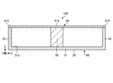
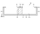
図1は、実施の形態1にかかる電力半導体装置100の構成を示す平面図である。図2は、実施の形態1にかかる電力半導体装置100の構成を示す第1の断面図であり、図1におけるII-II線に沿った断面図である。図3は、実施の形態1にかかる電力半導体装置100の構成を示す第2の断面図であり、図1におけるIII-III線に沿った断面図である。なお、断面図については、見やすくするために一部のハッチングを省略している。Embodiment 1.
Fig. 1 is a plan view showing a configuration of apower semiconductor device 100 according to a first embodiment. Fig. 2 is a first cross-sectional view showing the configuration of the power semiconductor device 100 according to the first embodiment, which is a cross-sectional view taken along line II-II in Fig. 1. Fig. 3 is a second cross-sectional view showing the configuration of the power semiconductor device 100 according to the first embodiment, which is a cross-sectional view taken along line III-III in Fig. 1. Note that some hatching has been omitted from the cross-sectional view to make it easier to see.
図1は、実施の形態1にかかる電力半導体装置100の構成を示す平面図である。図2は、実施の形態1にかかる電力半導体装置100の構成を示す第1の断面図であり、図1におけるII-II線に沿った断面図である。図3は、実施の形態1にかかる電力半導体装置100の構成を示す第2の断面図であり、図1におけるIII-III線に沿った断面図である。なお、断面図については、見やすくするために一部のハッチングを省略している。
Fig. 1 is a plan view showing a configuration of a
実施の形態1においては、図1から図3における左右方向を、電力半導体装置100および電力半導体装置100の構成部の左右方向とする。左右方向は、図1から図3におけるX方向に対応し、電力半導体装置100および電力半導体装置100の構成部の幅方向に対応する。また、図2および図3における紙面の奥行方向、および図1における上下方向を、電力半導体装置100および電力半導体装置100の構成部の奥行方向とする。奥行方向は、図1から図3におけるY方向に対応し、電力半導体装置100および電力半導体装置100の構成部の奥行方向に対応する。また、奥行方向は、不図示の送風システムから電力半導体装置100に送風される空気流200の進行方向、すなわち送風方向あるいは電力半導体装置100における風流入方向と換言できる。また、奥行方向は、保持部60の内部における空気流200の進行方向と換言できる。また、図2および図3における上下方向および図1における紙面の奥行方向を、電力半導体装置100および電力半導体装置100の構成部の上下方向とする。上下方向は、図1から図3におけるZ方向に対応し、電力半導体装置100および電力半導体装置100の構成部の高さ方向に対応する。
In the first embodiment, the left-right direction in FIG. 1 to FIG. 3 is the left-right direction of the power semiconductor device 100 and the components of the power semiconductor device 100. The left-right direction corresponds to the X direction in FIG. 1 to FIG. 3 and corresponds to the width direction of the power semiconductor device 100 and the components of the power semiconductor device 100. The depth direction of the paper in FIG. 2 and FIG. 3 and the up-down direction in FIG. 1 are the depth direction of the power semiconductor device 100 and the components of the power semiconductor device 100. The depth direction corresponds to the Y direction in FIG. 1 to FIG. 3 and corresponds to the depth direction of the power semiconductor device 100 and the components of the power semiconductor device 100. The depth direction can be rephrased as the traveling direction of the air flow 200 blown from the blowing system (not shown) to the power semiconductor device 100, that is, the blowing direction or the wind inflow direction in the power semiconductor device 100. The depth direction can be rephrased as the traveling direction of the air flow 200 inside the holding portion 60. The up-down direction in FIG. 2 and FIG. 3 and the depth direction of the paper in FIG. 1 are the up-down direction of the power semiconductor device 100 and the components of the power semiconductor device 100. The up-down direction corresponds to the Z direction in Figures 1 to 3, and corresponds to the height direction of the power semiconductor device 100 and the components of the power semiconductor device 100.
また、図2および図3の紙面の奥行方向における手前側、および図1の下側を、電力半導体装置100およびヒートシンク一体型パワーモジュール20の正面側とする。図2および図3の紙面の奥行方向における奥側、および図1の上側を、電力半導体装置100およびヒートシンク一体型パワーモジュール20の背面側とする。なお、「左右」、「上下」、「正面」および「背面」の表現は、便宜上の記載であり、実際の「左右」、「上下」、「正面」および「背面」を意味するものではなく、これらの方向は逆とされてよい。
Furthermore, the near side in the depth direction of the paper of Figures 2 and 3, and the lower side of Figure 1, are the front sides of the power semiconductor device 100 and the heat sink integrated power module 20. The far side in the depth direction of the paper of Figures 2 and 3, and the upper side of Figure 1, are the rear sides of the power semiconductor device 100 and the heat sink integrated power module 20. Note that the expressions "left and right", "up and down", "front" and "rear" are used for convenience and do not mean the actual "left and right", "up and down", "front" and "rear", and these directions may be reversed.
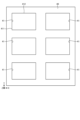
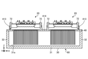
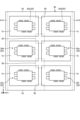
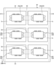
電力半導体装置100は、複数のヒートシンク一体型パワーモジュール20が保持部60に搭載されている。電力半導体装置100は、複数のヒートシンク一体型パワーモジュール20と、構造支持部50と、保持部60と、を備える。図1においては、実施の形態1にかかる複数のヒートシンク一体型パワーモジュール20が搭載された電力半導体装置の一例として、2列×3行に配列された6個のヒートシンク一体型パワーモジュール20が搭載された電力半導体装置100について示している。
The power semiconductor device 100 has multiple heat sink integrated power modules 20 mounted on a holding portion 60. The power semiconductor device 100 includes multiple heat sink integrated power modules 20, a structural support portion 50, and a holding portion 60. FIG. 1 shows a power semiconductor device 100 mounted with six heat sink integrated power modules 20 arranged in two columns and three rows, as an example of a power semiconductor device mounted with multiple heat sink integrated power modules 20 according to the first embodiment.
保持部60は、電力半導体装置100において複数のヒートシンク一体型パワーモジュール20の一部を収納して保持する。すなわち、複数のヒートシンク一体型パワーモジュール20は、一部分が保持部60に収納された状態で保持部60に保持されている。保持部60は、ハウジング40と外枠30とにより構成されている。
The holding portion 60 houses and holds a portion of the multiple heat sink integrated power modules 20 in the power semiconductor device 100. That is, the multiple heat sink integrated power modules 20 are held in the holding portion 60 with a portion of each module housed in the holding portion 60. The holding portion 60 is composed of a housing 40 and an outer frame 30.
図1に示す電力半導体装置100においては、ヒートシンク一体型パワーモジュール20である、ヒートシンク一体型パワーモジュール20a、ヒートシンク一体型パワーモジュール20b、ヒートシンク一体型パワーモジュール20c、ヒートシンク一体型パワーモジュール20d、ヒートシンク一体型パワーモジュール20e、およびヒートシンク一体型パワーモジュール20fが保持部60に取り付けられている。なお、電力半導体装置100におけるヒートシンク一体型パワーモジュール20の取付個数は6個に限定されない。例えば、左右方向において2つ以上のヒートシンク一体型パワーモジュール20が保持部60に取り付けられてもよい。このような形態においても、後述する電力半導体装置100の効果が得られる。
In the power semiconductor device 100 shown in FIG. 1, the heatsink-integrated power modules 20, namely, heatsink-integrated power module 20a, heatsink-integrated power module 20b, heatsink-integrated power module 20c, heatsink-integrated power module 20d, heatsink-integrated power module 20e, and heatsink-integrated power module 20f, are attached to a holding portion 60. Note that the number of heatsink-integrated power modules 20 attached to the power semiconductor device 100 is not limited to six. For example, two or more heatsink-integrated power modules 20 may be attached to the holding portion 60 in the left-right direction. Even in this configuration, the effects of the power semiconductor device 100 described below can be obtained.
保持部60の内部には、送風システムから送風される空気流200が、正面側から背面側に向かって流れる。なお、空気流200が流れる方向は、背面側から正面側に向かう方向であってもよい。
Inside the holding unit 60, the air flow 200 blown from the ventilation system flows from the front side to the rear side. Note that the direction in which the air flow 200 flows may also be from the rear side to the front side.
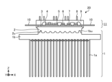
ヒートシンク一体型パワーモジュール20は、電力半導体装置100に搭載される電力半導体モジュールであり、樹脂モールドタイプのパワーモジュールである。図4は、実施の形態1にかかるヒートシンク一体型パワーモジュール20の断面図である。実施の形態1にかかるヒートシンク一体型パワーモジュール20は、ヒートシンク1と、フィンベース2と、絶縁シート3と、配線ワイヤ4と、半導体素子5と、はんだ6と、金属導体7と、制御端子8と、封止樹脂9と、主端子10と、を備える。
The heat sink integrated power module 20 is a power semiconductor module mounted on the power semiconductor device 100, and is a resin molded type power module. FIG. 4 is a cross-sectional view of the heat sink integrated power module 20 according to the first embodiment. The heat sink integrated power module 20 according to the first embodiment includes a heat sink 1, a fin base 2, an insulating sheet 3, wiring wires 4, a semiconductor element 5, solder 6, a metal conductor 7, a control terminal 8, a sealing resin 9, and a main terminal 10.
また、ヒートシンク1は、複数の放熱フィン1aと、ヒートシンクベース1bと、を有する。また、絶縁シート3、配線ワイヤ4、半導体素子5、はんだ6、金属導体7、制御端子8、封止樹脂9および主端子10により、実施の形態1にかかるパワーモジュール11が構成されている。したがって、実施の形態1にかかるヒートシンク一体型パワーモジュール20は、ヒートシンク1と、パワーモジュール11とがフィンベース2を介して接合されて構成されている。すなわち、ヒートシンク一体型パワーモジュール20は、パワーモジュール11と、複数の放熱フィン1aがヒートシンクベース1bに設けられてパワーモジュール11で発生した熱を放熱するヒートシンク1とが一体とされている。
The heat sink 1 also has a plurality of heat dissipation fins 1a and a heat sink base 1b. The power module 11 according to the first embodiment is composed of the insulating sheet 3, wiring wires 4, semiconductor element 5, solder 6, metal conductor 7, control terminal 8, sealing resin 9 and main terminal 10. Therefore, the heat sink integrated power module 20 according to the first embodiment is composed of the heat sink 1 and the power module 11 joined via the fin base 2. That is, the heat sink integrated power module 20 is composed of the power module 11 and the heat sink 1, which has a plurality of heat dissipation fins 1a provided on the heat sink base 1b and dissipates heat generated by the power module 11, which are integrated together.
ヒートシンク一体型パワーモジュール20は、パワーモジュール11の下面側に、ヒートシンク1が接続されて、パワーモジュール11の半導体素子5において発生した熱の放熱の向上が図られている。すなわち、ヒートシンク一体型パワーモジュール20は、パワーモジュール11の半導体素子5での発熱をヒートシンク1から放熱することにより、パワーモジュール11において発生した熱の放熱の向上が図られている。そして、ヒートシンク一体型パワーモジュール20は、パワーモジュール11とヒートシンク1との間に熱伝導性グリスを使用しないグリスレスパワーモジュールである。このため、ヒートシンク一体型パワーモジュール20は、パワーモジュール11とヒートシンク1との間に熱伝導性グリスを使用する場合と比べて、パワーモジュール11において発生した熱の放熱特性がより高められており、より高い放熱性能を有する。
The heat sink integrated power module 20 has a heat sink 1 connected to the underside of the power module 11, improving the dissipation of heat generated in the semiconductor element 5 of the power module 11. That is, the heat sink integrated power module 20 improves the dissipation of heat generated in the power module 11 by dissipating heat generated in the semiconductor element 5 of the power module 11 from the heat sink 1. The heat sink integrated power module 20 is a greaseless power module that does not use thermally conductive grease between the power module 11 and the heat sink 1. Therefore, the heat sink integrated power module 20 has improved heat dissipation characteristics for heat generated in the power module 11 compared to when thermally conductive grease is used between the power module 11 and the heat sink 1, and has higher heat dissipation performance.
ヒートシンク1は、放熱フィン1aとヒートシンクベース1bとが「かしめ加工」により一体化された、かしめ加工ヒートシンクである。
The heat sink 1 is a crimped heat sink in which the heat dissipation fins 1a and the heat sink base 1b are integrated by crimping.
放熱フィン1aは、矩形形状を有する薄板状の放熱部品である。放熱フィン1aは、パワーモジュール11の半導体素子5での発熱を放熱することができるように、熱伝導性が相対的に高い金属材料によって構成されている。一例では、放熱フィン1aは、アルミニウムおよびアルミニウム合金といった腐食し難い金属材料により構成される。放熱フィン1aに上述したアルミニウム等の金属材料の圧延材が用いられることにより、放熱フィン1aの加工性と、半導体素子5での発熱の放熱性と、を両立させることができる。
The heat dissipation fin 1a is a thin plate-like heat dissipation component having a rectangular shape. The heat dissipation fin 1a is made of a metal material with relatively high thermal conductivity so that it can dissipate heat generated in the semiconductor element 5 of the power module 11. In one example, the heat dissipation fin 1a is made of a metal material that is resistant to corrosion, such as aluminum or an aluminum alloy. By using a rolled material of a metal material such as aluminum described above for the heat dissipation fin 1a, it is possible to achieve both the ease of processing the heat dissipation fin 1a and the ability to dissipate heat generated in the semiconductor element 5.
複数の放熱フィン1aの各々は、ヒートシンクベース1bにおける一面側に形成された不図示のフィン挿入溝に挿入され、かしめられることによって、ヒートシンクベース1bに固定されている。放熱フィン1aは、ヒートシンクベース1bをフィンベース2と挟み込むように配置される。
Each of the multiple heat dissipation fins 1a is inserted into a fin insertion groove (not shown) formed on one side of the heat sink base 1b and is fixed to the heat sink base 1b by crimping. The heat dissipation fins 1a are arranged so that the heat sink base 1b is sandwiched between the fin base 2.
ヒートシンクベース1bは、当該ヒートシンクベース1bの面内方向において矩形形状を有する平板状の部品であり、複数の放熱フィン1aが固定されてヒートシンク1のベースとなる部品である。ヒートシンクベース1bは、パワーモジュール11の半導体素子5での発熱を放熱フィン1aに効率良く伝熱できるように、熱伝導性が相対的に高い金属材料によって構成されている。一例では、ヒートシンクベース1bは、アルミニウムおよびアルミニウム合金といった腐食し難い金属材料によって構成される。ヒートシンクベース1bは、切削加工、ダイキャスト加工、鍛造加工、押出加工などの加工方法によって作製される。
The heat sink base 1b is a flat part having a rectangular shape in the in-plane direction of the heat sink base 1b, and is a part to which a plurality of heat dissipation fins 1a are fixed, forming the base of the heat sink 1. The heat sink base 1b is made of a metal material with relatively high thermal conductivity so that heat generated in the semiconductor element 5 of the power module 11 can be efficiently transferred to the heat dissipation fins 1a. In one example, the heat sink base 1b is made of a metal material that is resistant to corrosion, such as aluminum and aluminum alloys. The heat sink base 1b is manufactured by a processing method such as cutting, die casting, forging, and extrusion.
フィンベース2は、ヒートシンクベース1bよりも小さい矩形形状を有する平板状の部品であり、パワーモジュール11とヒートシンク1とを接続する接続部品である。フィンベース2は、パワーモジュール11の半導体素子5での発熱をパワーモジュール11からヒートシンク1に効率良く伝熱できるように、熱伝導性が相対的に高い金属材料によって構成されている。一例では、フィンベース2は、アルミニウムおよびアルミニウム合金といった腐食し難い金属材料によって構成される。フィンベース2は、切削加工、ダイキャスト加工、鍛造加工、押出加工などの加工方法によって作製される。
The fin base 2 is a flat rectangular plate-like part smaller than the heat sink base 1b, and is a connecting part that connects the power module 11 and the heat sink 1. The fin base 2 is made of a metal material with relatively high thermal conductivity so that heat generated in the semiconductor element 5 of the power module 11 can be efficiently transferred from the power module 11 to the heat sink 1. In one example, the fin base 2 is made of a metal material that is resistant to corrosion, such as aluminum or an aluminum alloy. The fin base 2 is manufactured by a processing method such as cutting, die casting, forging, or extrusion.
なお、放熱フィン1a、ヒートシンクベース1bおよびフィンベース2の各々の材料は、ともに上述したアルミニウム系材料に限定されるものではなく、他の材料であってもよい。すなわち、放熱フィン1aとヒートシンクベース1bとフィンベース2との材料の組み合わせは、上記とは異なる材料の組み合わせであってもよい。例えば、放熱能力の観点では、放熱フィン1aをアルミニウム系材料よりも熱伝導率が大きい銅系の板部品とすることで、放熱フィン1aがアルミニウム系材料からなる板部品である場合よりも、さらに放熱フィン1aの放熱能力が向上する。
The materials of the heat dissipation fins 1a, heat sink base 1b, and fin base 2 are not limited to the aluminum-based materials described above, and may be other materials. In other words, the combination of materials of the heat dissipation fins 1a, heat sink base 1b, and fin base 2 may be a combination of materials different from those described above. For example, from the perspective of heat dissipation capacity, by making the heat dissipation fins 1a out of a copper-based plate component, which has a higher thermal conductivity than an aluminum-based material, the heat dissipation capacity of the heat dissipation fins 1a is improved even more than when the heat dissipation fins 1a are plate components made of an aluminum-based material.
放熱フィン1aとヒートシンクベース1bとがかしめ加工により一体化されたかしめ加工ヒートシンクをヒートシンク1に採用する場合には、ダイキャスト加工および押出加工でヒートシンクを作製する場合のアスペクト比の加工制約がないため、放熱フィン1aを自由に設計することができ、ヒートシンク1の放熱能力を向上させることができる。ただし、ヒートシンク1は、かしめ加工ヒートシンクに限定されず、他の加工方法によって作製されたヒートシンクが用いられてもよい。
When a crimped heat sink in which the heat dissipation fins 1a and the heat sink base 1b are integrated by crimping is used for the heat sink 1, there are no processing restrictions on the aspect ratio that exist when producing a heat sink by die casting or extrusion, so the heat dissipation fins 1a can be designed freely and the heat dissipation capacity of the heat sink 1 can be improved. However, the heat sink 1 is not limited to a crimped heat sink, and heat sinks produced by other processing methods may also be used.
図5は、実施の形態1にかかる第1の変形例のヒートシンク12が取り付けられた第1の変形例のヒートシンク一体型パワーモジュールの断面図である。図5においては、図4と同じ構成については、同じ符号を付している。第1の変形例のヒートシンク12は、押出加工によって放熱フィン1aとヒートシンクベース1bとが一体に作製されている。
FIG. 5 is a cross-sectional view of a heat sink-integrated power module of a first modified example to which a heat sink 12 of a first modified example according to embodiment 1 is attached. In FIG. 5, the same components as in FIG. 4 are given the same reference numerals. In the heat sink 12 of the first modified example, the heat dissipation fins 1a and the heat sink base 1b are integrally manufactured by extrusion processing.
図6は、実施の形態1にかかる第2の変形例のヒートシンク13が取り付けられた第2の変形例のヒートシンク一体型パワーモジュールの断面図である。図6においては、図4と同じ構成については、同じ符号を付している。第2の変形例のヒートシンク13は、ダイキャスト加工によって放熱フィン1aとヒートシンクベース1bとが一体に作製されている。
FIG. 6 is a cross-sectional view of a heat sink-integrated power module of a second modified example to which a heat sink 13 of a second modified example according to the first embodiment is attached. In FIG. 6, the same components as in FIG. 4 are given the same reference numerals. In the heat sink 13 of the second modified example, the heat dissipation fins 1a and the heat sink base 1b are integrally produced by die casting.
また、ヒートシンク一体型パワーモジュール20においては、切削加工あるいは鍛造加工で作製されたヒートシンクが用いられてもよい。
In addition, in the heat sink integrated power module 20, a heat sink made by cutting or forging may be used.
図7は、実施の形態1にかかる第3の変形例のヒートシンク一体型パワーモジュールの断面図である。第3の変形例のヒートシンク一体型パワーモジュールは、パワーモジュール11とヒートシンク1とが、はんだといった接合材15あるいは接着剤16によって接続しされている。
FIG. 7 is a cross-sectional view of a heat sink-integrated power module of a third modified example according to the first embodiment. In the heat sink-integrated power module of the third modified example, the power module 11 and the heat sink 1 are connected by a bonding material 15 such as solder or an adhesive 16.
図5から図7に示す構造においても、上述したように高い放熱性能を実現できるというグリスレスパワーモジュールの効果が得られる。
Even with the structures shown in Figures 5 to 7, the effect of a greaseless power module that can achieve high heat dissipation performance as described above can be obtained.
絶縁シート3は、封止樹脂9に封止された構成部とヒートシンクベース1bとを絶縁すると共に、半導体素子5が発生させた熱をヒートシンクベース1bに放熱する。絶縁シート3は、封止樹脂9と同等以上の放熱性を有する。
The insulating sheet 3 insulates the components sealed in the sealing resin 9 from the heat sink base 1b, and dissipates heat generated by the semiconductor element 5 to the heat sink base 1b. The insulating sheet 3 has heat dissipation properties equal to or greater than those of the sealing resin 9.
配線ワイヤ4は、半導体素子5同士を電気的に接続し、また、半導体素子5と主端子10とを電気的に接続する。
The wiring wires 4 electrically connect the semiconductor elements 5 to each other and also electrically connect the semiconductor elements 5 to the main terminals 10.
半導体素子5は、電力制御用の半導体素子である。半導体素子5の一例は、整流ダイオード、パワートランジスタ、サイリスタ、IGBT(Insulated Gate Bipolar Transistor)である。半導体素子5は、珪素(Si)によって形成される素子、または珪素に比べてバンドギャップが大きいワイドバンドギャップ半導体によって形成される素子が例示される。ワイドバンドギャップ半導体の一例は、炭化珪素(SiC)、窒化ガリウム系材料またはダイヤモンドである。ワイドバンドギャップ半導体を用いた半導体素子5は、許容電流密度が高く、電力損失が低いため、ヒートシンク一体型パワーモジュール20および電力半導体装置100を小型化することができる。
The semiconductor element 5 is a semiconductor element for power control. Examples of the semiconductor element 5 are a rectifier diode, a power transistor, a thyristor, and an IGBT (Insulated Gate Bipolar Transistor). The semiconductor element 5 is exemplified by an element formed of silicon (Si), or an element formed of a wide band gap semiconductor having a larger band gap than silicon. Examples of wide band gap semiconductors are silicon carbide (SiC), gallium nitride-based materials, and diamond. The semiconductor element 5 using a wide band gap semiconductor has a high allowable current density and low power loss, and therefore the heat sink-integrated power module 20 and the power semiconductor device 100 can be made smaller.
はんだ6は、半導体素子5と金属導体7とを接合する接合材である。なお、半導体素子5と金属導体7とを接合する接合材は、はんだ6に限定されない。
The solder 6 is a bonding material that bonds the semiconductor element 5 and the metal conductor 7. Note that the bonding material that bonds the semiconductor element 5 and the metal conductor 7 is not limited to the solder 6.
金属導体7は、半導体素子5が搭載される基板であり、半導体素子5が発生させた熱を絶縁シート3に放熱する。
The metal conductor 7 is a substrate on which the semiconductor element 5 is mounted, and dissipates heat generated by the semiconductor element 5 to the insulating sheet 3.
制御端子8および主端子10は、半導体素子5に接続され、半導体素子5に電力を供給し、または半導体素子5と外部の装置との間で信号の伝送を行う。
The control terminal 8 and the main terminal 10 are connected to the semiconductor element 5 to supply power to the semiconductor element 5 or transmit signals between the semiconductor element 5 and an external device.
封止樹脂9は、パワーモジュール11の筐体を構成する。封止樹脂9は、エポキシなどの熱硬化性樹脂により形成され、内部に配置された部材間の絶縁性を確保する。封止樹脂9は、例えばトランスファー成型によって形成されたトランスファーモールドである。ただし、封止樹脂9の成型方法は、トランスファー成型に限定されない。
The sealing resin 9 constitutes the housing of the power module 11. The sealing resin 9 is made of a thermosetting resin such as epoxy, and ensures insulation between the components arranged inside. The sealing resin 9 is a transfer mold formed by transfer molding, for example. However, the molding method of the sealing resin 9 is not limited to transfer molding.
つぎに、上記のように構成されたヒートシンク一体型パワーモジュール20の製造方法について説明する。
Next, a method for manufacturing the heat sink-integrated power module 20 configured as described above will be described.
まず、半導体素子5が、はんだ6を用いて金属導体7にダイボンドされる。つぎに、半導体素子5と他の半導体素子5とが、配線ワイヤ4によりワイヤボンドされ、電気的に接続される。また、一部の半導体素子5と、制御端子8または主端子10とが、配線ワイヤ4によりワイヤボンドされ、電気的に接続される。つぎに、絶縁シート3が、フィンベース2の一面上に仮付けされる。
First, the semiconductor element 5 is die-bonded to the metal conductor 7 using solder 6. Next, the semiconductor element 5 is wire-bonded to other semiconductor elements 5 by wiring wires 4, and electrically connected. In addition, some of the semiconductor elements 5 are wire-bonded to the control terminals 8 or the main terminals 10 by wiring wires 4, and electrically connected. Next, the insulating sheet 3 is temporarily attached onto one surface of the fin base 2.
その後、絶縁シート3が一面上に仮付けされたフィンベース2と、上述したように半導体素子5のダイボンドおよび配線ワイヤ4のワイヤボンドが完了した金属導体7と、制御端子8および主端子10とが封止樹脂9を用いて一体化されることにより、ヒートシンク一体型パワーモジュール20とフィンベース2とが組み立てられた組立体が作製される。
Then, the fin base 2 with the insulating sheet 3 temporarily attached on one side, the metal conductor 7 on which the die bonding of the semiconductor element 5 and the wire bonding of the wiring wire 4 have been completed as described above, the control terminal 8 and the main terminal 10 are integrated using sealing resin 9 to produce an assembly in which the heat sink-integrated power module 20 and the fin base 2 are assembled.
さらに、フィンベース2における他面側に設けられたフィンベース凹凸部2uと、ヒートシンクベース1bの一面に設けられたヒートシンクベース凹凸部1buとが、プレス加工によって嵌合固定されることにより、組立体とヒートシンクベース1bとが一体化される。これにより、図1に示すヒートシンク一体型パワーモジュール20が形成される。
Furthermore, the fin base uneven portion 2u provided on the other side of the fin base 2 and the heat sink base uneven portion 1bu provided on one side of the heat sink base 1b are fitted and fixed by press processing, thereby integrating the assembly with the heat sink base 1b. This forms the heat sink integrated power module 20 shown in FIG. 1.
上述したヒートシンク一体型パワーモジュール20の製造方法においては、プレス加工によりフィンベース2とヒートシンクベース1bとが一体化されるため、プレス加工時の半導体素子5へのダメージ、半導体素子5の割れ、半導体素子5の特性変化、封止樹脂9の割れ、絶縁シート3の耐圧低下、その他、ヒートシンク一体型パワーモジュール20の各部材間の剥離などの不具合の発生が懸念される。このため、組立体とヒートシンクベース1bとを一体化する際のプレス荷重は、できる限り低荷重であることが好ましい。
In the manufacturing method of the heat sink integrated power module 20 described above, the fin base 2 and the heat sink base 1b are integrated by pressing, so there is concern that problems such as damage to the semiconductor element 5 during pressing, cracking of the semiconductor element 5, changes in the characteristics of the semiconductor element 5, cracking of the sealing resin 9, a decrease in the pressure resistance of the insulating sheet 3, and peeling between the various components of the heat sink integrated power module 20 may occur. For this reason, it is preferable that the press load when integrating the assembly and the heat sink base 1b is as low as possible.
図8は、実施の形態1にかかる電力半導体装置100の外枠30を示す上面図である。図9は、実施の形態1にかかる電力半導体装置100の外枠30を示す断面図であり、図8におけるIX-IX線に沿った断面図である。
FIG. 8 is a top view showing the outer frame 30 of the power semiconductor device 100 according to the first embodiment. FIG. 9 is a cross-sectional view showing the outer frame 30 of the power semiconductor device 100 according to the first embodiment, taken along line IX-IX in FIG. 8.
外枠30は、ヒートシンク一体型パワーモジュール20が取り付けられたハウジング40を支持し、また送風システムから送風される空気流200の風路を形成する。外枠30は、当該外枠30の底面部31における左右方向の両端部から2つの側面部32が垂直上方に立ち上がり、上側、正面側および背面側が解放された直方体形状の箱形状を有する。すなわち、外枠30は、図2、図3、図8および図9に示すように、左右方向に沿った断面においてU形状の断面形状を有し、ハウジング40が取り付けられる上面側、正面側および背面側の面以外の面が閉じた構造となっている。なお、外枠30は、上面側、正面側および背面側の面以外の面も必ずしも閉じた形状である必要はなく、必要に応じて開口部が形成されてもよい。
The outer frame 30 supports the housing 40 to which the heat sink-integrated power module 20 is attached, and forms an air passage for the air flow 200 blown from the air blowing system. The outer frame 30 has two side sections 32 rising vertically upward from both left and right ends of the bottom surface 31 of the outer frame 30, and has a rectangular box shape with the top, front and back sides open. That is, as shown in Figures 2, 3, 8 and 9, the outer frame 30 has a U-shaped cross section in the left and right direction, and has a structure in which all sides except the top, front and back sides to which the housing 40 is attached are closed. Note that the outer frame 30 does not necessarily have to have a closed shape on all sides other than the top, front and back sides, and openings may be formed as necessary.
また、「U形状」とは、角が無い形状だけでなく、図2、図3、図8および図9に示すように、角がある形状も含むものである。すなわち、「U形状」は、曲がっている部分が曲線によって連続的に構成されている形状と、曲がっている部分が屈曲部により構成されている形状とを含む。
Furthermore, "U-shape" includes not only shapes without corners, but also shapes with corners, as shown in Figures 2, 3, 8, and 9. In other words, "U-shape" includes shapes in which the curved portion is made up of a continuous curve, and shapes in which the curved portion is made up of a bend.
外枠30では、底面部31および2つの側面部32により囲まれた内部空間が、送風システムから送風される風の風路を構成している。外枠30は、解放された正面側が、送風システムから送風される風の流入口とされている。また、外枠30は、解放された背面側が、流入口から外枠30の内部に流入して外枠30の内部を流れた風の流出口とされている。外枠30における風の流入口は、保持部60における風の流入口と換言できる。外枠30における風の流出口は、保持部60における風の流出口と換言できる。
In the outer frame 30, the internal space surrounded by the bottom portion 31 and the two side portions 32 forms an air passage for the air blown from the air blowing system. The open front side of the outer frame 30 serves as an inlet for the air blown from the air blowing system. The open back side of the outer frame 30 serves as an outlet for the air that flows from the inlet into the outer frame 30 and through the interior of the outer frame 30. The air inlet in the outer frame 30 can be said as the air inlet in the holding portion 60. The air outlet in the outer frame 30 can be said as the air outlet in the holding portion 60.
外枠30は、ハウジング40、ヒートシンク一体型パワーモジュール20、およびヒートシンク一体型パワーモジュール20に接続される各部品の自重を支えるため、上記の構成部を支持できる剛性を有する材料によって構成される。また、外枠30は、電力半導体装置100の製品重量の観点から、上記の構成部を支持できる剛性を有する範囲で、できる限り薄くされて軽量化されることが好ましい。例えば、メッキ鋼板は、上記の構成部を支持できる剛性、薄肉化および軽量化をともに実現可能であり、外枠30に用いられる材料として好ましい材料である。なお、外枠30には、メッキ鋼板以外の材料を用いることも可能である。
The outer frame 30 is made of a material having the rigidity to support the above components in order to support the weight of the housing 40, the heat sink integrated power module 20, and each component connected to the heat sink integrated power module 20. From the viewpoint of the product weight of the power semiconductor device 100, it is preferable that the outer frame 30 is as thin and lightweight as possible while still having the rigidity to support the above components. For example, plated steel sheet is a preferable material for the outer frame 30 because it can achieve the rigidity to support the above components, as well as thinness and weight reduction. It is also possible to use materials other than plated steel sheet for the outer frame 30.
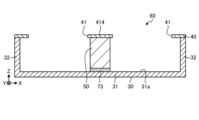
ハウジング40は、ヒートシンク一体型パワーモジュール20が取り付けられて搭載される、ヒートシンク一体型パワーモジュール20の取付板である。ハウジング40は、図2および図3に示すように、外枠30の2つの側面部32上に載置される。ハウジング40の面内方向と、外枠30の底面部31の面内方向と、ヒートシンク一体型パワーモジュール20のヒートシンクベース1bの面内方向とは平行とされている。
The housing 40 is a mounting plate for the heat sink-integrated power module 20 on which the heat sink-integrated power module 20 is attached and mounted. As shown in Figures 2 and 3, the housing 40 is placed on the two side surfaces 32 of the outer frame 30. The in-plane direction of the housing 40, the in-plane direction of the bottom surface 31 of the outer frame 30, and the in-plane direction of the heat sink base 1b of the heat sink-integrated power module 20 are parallel to each other.
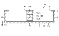
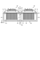
図10は、実施の形態1にかかる電力半導体装置100のハウジング40を示す上面図である。図10に示すように、ハウジング40は、板形状を有し、ヒートシンク一体型パワーモジュール20の一部分が挿入される複数の開口部41が形成されている。ハウジング40には、搭載されるヒートシンク一体型パワーモジュール20の数、放熱フィン1aのサイズに対応した複数の開口部41が形成されている。図10に示すハウジング40では、6つのヒートシンク一体型パワーモジュール20を搭載するために、6個の開口部41が形成されている。
FIG. 10 is a top view showing the housing 40 of the power semiconductor device 100 according to the first embodiment. As shown in FIG. 10, the housing 40 has a plate shape and is formed with a number of openings 41 into which a portion of the heat sink integrated power module 20 is inserted. The housing 40 is formed with a number of openings 41 corresponding to the number of heat sink integrated power modules 20 to be mounted and the size of the heat dissipation fins 1a. In the housing 40 shown in FIG. 10, six openings 41 are formed in order to mount six heat sink integrated power modules 20.
開口部41は、ハウジング40の面内方向において、長方形状を有する。なお、開口部41の形状は長方形状に限定されず、ヒートシンク一体型パワーモジュール20の形状に合わせて形成されればよい。開口部41は、ハウジング40の面内方向において、ヒートシンク一体型パワーモジュール20の放熱フィン1aの全体が挿入可能な大きさを有し、且つヒートシンクベース1bの外周縁部1bpが挿通できない大きさを有する。すなわち、開口部41は、ハウジング40の面内方向において、ヒートシンク一体型パワーモジュール20の放熱フィン1aの全体が挿入可能であるが、ヒートシンクベース1bが挿通できない寸法および形状を有する。開口部41、ヒートシンク一体型パワーモジュール20、ヒートシンクベース1bおよび放熱フィン1aの大きさの関係については、後述する。
The opening 41 has a rectangular shape in the in-plane direction of the housing 40. The shape of the opening 41 is not limited to a rectangular shape, and may be formed to match the shape of the heat sink integrated power module 20. The opening 41 has a size in the in-plane direction of the housing 40 that allows the entire heat dissipation fin 1a of the heat sink integrated power module 20 to be inserted, but has a size that does not allow the outer peripheral edge portion 1bp of the heat sink base 1b to be inserted. In other words, the opening 41 has a size and shape in the in-plane direction of the housing 40 that allows the entire heat dissipation fin 1a of the heat sink integrated power module 20 to be inserted, but does not allow the heat sink base 1b to be inserted. The relationship in size between the opening 41, the heat sink integrated power module 20, the heat sink base 1b, and the heat dissipation fin 1a will be described later.
ハウジング40は、ヒートシンク一体型パワーモジュール20およびヒートシンク一体型パワーモジュール20に接続される各部品の自重を支えるため、上記の構成部を支持できる剛性を有する材料によって構成される。また、ハウジング40は、電力半導体装置100の製品重量の観点から、上記の構成部を支持できる剛性を有する範囲で、できる限り薄くされて軽量化されることが好ましい。例えば、メッキ鋼板は、上記の構成部を支持できる剛性、薄肉化および軽量化をともに実現可能であり、ハウジング40に用いられる材料として好ましい材料である。なお、ハウジング40には、メッキ鋼板以外の材料を用いることも可能である。
The housing 40 is made of a material having the rigidity to support the above components in order to support the weight of the heat sink integrated power module 20 and each component connected to the heat sink integrated power module 20. From the viewpoint of the product weight of the power semiconductor device 100, it is preferable that the housing 40 is as thin and lightweight as possible while still having the rigidity to support the above components. For example, plated steel sheet is a preferable material for the housing 40 because it can achieve the rigidity to support the above components, as well as thinness and weight reduction. It is also possible to use materials other than plated steel sheet for the housing 40.
複数の開口部41には、図2に示すように、ヒートシンク一体型パワーモジュール20のヒートシンク1の放熱フィン1aが保持部60の外部側から挿入される。ハウジング40は、放熱フィン1aが保持部60の内部に収納された状態で、ヒートシンクベース1bの外周縁部1bpが、開口部41に隣接する隣接領域413に載置されている。そして、ハウジング40は、外枠30のU形状における自由端である2つの側面部32の端部に支持されて保持部60の一面を構成する。
As shown in FIG. 2, the heat dissipation fins 1a of the heat sink 1 of the heat sink-integrated power module 20 are inserted into the multiple openings 41 from the outside of the holding portion 60. With the heat dissipation fins 1a stored inside the holding portion 60, the housing 40 has the outer peripheral edge portion 1bp of the heat sink base 1b placed on the adjacent region 413 adjacent to the openings 41. The housing 40 is supported by the ends of the two side portions 32, which are the free ends of the U-shape of the outer frame 30, and forms one side of the holding portion 60.
これにより、ハウジング40は、隣接領域413においてヒートシンクベース1bを保持することにより、ヒートシンク一体型パワーモジュール20を保持している。すなわち、複数のヒートシンク一体型パワーモジュール20は、複数の放熱フィン1aが開口部41から保持部60の内部に挿入され、ヒートシンクベース1bの面内方向において、ヒートシンクベース1bの外周縁部1bpが、保持部60の一面を構成するハウジング40において開口部41に隣接する隣接領域413上に支持されている。
As a result, the housing 40 holds the heatsink base 1b in the adjacent region 413, thereby holding the heatsink integrated power module 20. That is, the multiple heat dissipation fins 1a of the multiple heatsink integrated power modules 20 are inserted into the holding portion 60 from the opening 41, and the outer peripheral edge portion 1bp of the heatsink base 1b is supported on the adjacent region 413 adjacent to the opening 41 in the housing 40 that constitutes one surface of the holding portion 60 in the in-plane direction of the heatsink base 1b.
したがって、上述した構成を有する外枠30とハウジング40とにより構成される保持部60は、風の流入口と、風の流出口とが対向して設けられ、流入口と前記流出口とを繋ぐ一面を構成するハウジング40に複数の開口部41が形成された箱形状を有する。
Therefore, the holding section 60, which is constituted by the outer frame 30 and the housing 40 having the above-mentioned configuration, has a box shape with an air inlet and an air outlet facing each other, and multiple openings 41 formed in the housing 40 that constitutes one side connecting the air inlet and the air outlet.
構造支持部50は、保持部60の内部に設けられ、保持部60の一面を構成するハウジング40から保持部60の内部に向かう方向の荷重を受けて、ハウジング40およびハウジング40に搭載されたヒートシンク一体型パワーモジュール20を支持する。構造支持部50は、保持部60の幅方向において隣り合うヒートシンク一体型パワーモジュール20のヒートシンクベース1b同士の間に対応する位置に配置されている。保持部60の幅方向は、保持部60の流入口から保持部60の流出口に向かう方向と直交する方向であり、左右方向である。保持部60の流入口から保持部60の流出口に向かう方向は、Y方向に対応する。構造支持部50は、保持部60の流入口から保持部60の流出口までの領域において、流入口から流出口に向かう方向において連続して延在している。構造支持部50は、外枠30に固定され、上面がハウジング40と接している。構造支持部50は、長手方向に垂直な断面が長方形状を有する棒状とされている。なお、構造支持部50の形状は、構造支持部50の機能を発揮できれば限定されない。
The structural support portion 50 is provided inside the holding portion 60, and supports the housing 40 and the heat sink-integrated power module 20 mounted on the housing 40 by receiving a load from the housing 40 constituting one surface of the holding portion 60 toward the inside of the holding portion 60. The structural support portion 50 is disposed at a position corresponding to the space between the heat sink bases 1b of the heat sink-integrated power modules 20 adjacent to each other in the width direction of the holding portion 60. The width direction of the holding portion 60 is a direction perpendicular to the direction from the inlet of the holding portion 60 toward the outlet of the holding portion 60, and is a left-right direction. The direction from the inlet of the holding portion 60 toward the outlet of the holding portion 60 corresponds to the Y direction. The structural support portion 50 extends continuously in the direction from the inlet to the outlet in the region from the inlet of the holding portion 60 to the outlet of the holding portion 60. The structural support portion 50 is fixed to the outer frame 30, and the upper surface is in contact with the housing 40. The structural support portion 50 is rod-shaped with a rectangular cross section perpendicular to the longitudinal direction. The shape of the structural support part 50 is not limited as long as it can perform its function.
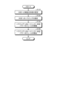
つぎに、上記のように構成された電力半導体装置100の製造方法について説明する。図11から図18は、実施の形態1にかかる電力半導体装置100の製造方法の手順の一例を模式的に示す図である。図19は、実施の形態1にかかる電力半導体装置100の製造方法の手順を示すフローチャートである。
Next, a method for manufacturing the power semiconductor device 100 configured as described above will be described. Figures 11 to 18 are diagrams that show an example of the steps of the method for manufacturing the power semiconductor device 100 according to the first embodiment. Figure 19 is a flowchart showing the steps of the method for manufacturing the power semiconductor device 100 according to the first embodiment.
まず、ステップS110において、構造支持部50が、外枠30に取り付けられて固定される。図11は、実施の形態1にかかる電力半導体装置100の製造方法の手順の一例を模式的に示す第1の上面図である。図12は、実施の形態1にかかる電力半導体装置100の製造方法の手順の一例を模式的に示す第1の断面図である。図12は、図11におけるXII-XII線に沿った断面図である。
First, in step S110, the structural support portion 50 is attached and fixed to the outer frame 30. FIG. 11 is a first top view that shows a schematic example of an exemplary procedure for the manufacturing method of the power semiconductor device 100 according to the first embodiment. FIG. 12 is a first cross-sectional view that shows a schematic example of an exemplary procedure for the manufacturing method of the power semiconductor device 100 according to the first embodiment. FIG. 12 is a cross-sectional view taken along line XII-XII in FIG. 11.
具体的に、図11および図12に示すように、構造支持部50が、外枠30における底面部31の内面31aに取り付けられて固定される。構造支持部50は、長手方向に垂直な断面が外枠30の底面部31の内面31aと垂直とされ、長手方向が外枠30の2つの側面部32に平行とされた状態で、底面部31の内面31aにおける左右方向の中央部に、取り付けられる。外枠30に対する構造支持部50の固定方法は、ネジ締めが例示される。なお、外枠30に対する構造支持部50の固定方法は、ネジ締めに限定されない。例えば、構造支持部50は、溶接により外枠30における底面部31の内面31aに固定されてもよい。
Specifically, as shown in Figures 11 and 12, the structural support part 50 is attached and fixed to the inner surface 31a of the bottom surface part 31 of the outer frame 30. The structural support part 50 is attached to the center part in the left-right direction of the inner surface 31a of the bottom surface part 31 with a cross section perpendicular to the longitudinal direction perpendicular to the inner surface 31a of the bottom surface part 31 of the outer frame 30 and with the longitudinal direction parallel to the two side surfaces 32 of the outer frame 30. An example of a method for fixing the structural support part 50 to the outer frame 30 is screw fastening. Note that the method for fixing the structural support part 50 to the outer frame 30 is not limited to screw fastening. For example, the structural support part 50 may be fixed to the inner surface 31a of the bottom surface part 31 of the outer frame 30 by welding.
つぎに、ステップS120において、ハウジング40が、ハウジング固定用ネジ71を用いて外枠30にネジ止めされて固定される。図13は、実施の形態1にかかる電力半導体装置100の製造方法の手順の一例を模式的に示す第2の上面図である。図14は、実施の形態1にかかる電力半導体装置100の製造方法の手順の一例を模式的に示す第2の断面図である。図15は、実施の形態1にかかる電力半導体装置100の製造方法の手順の一例を模式的に示す第3の断面図である。図16は、実施の形態1にかかる電力半導体装置100の製造方法の手順の一例を模式的に示す第3の上面図である。図17は、実施の形態1にかかる電力半導体装置100の製造方法の手順の一例を模式的に示す第4の上面図である。図14は、図13におけるXIIII-XIIII線に沿った断面図である。図15は、図13におけるXV-XV線に沿った断面図である。
Next, in step S120, the housing 40 is fixed to the outer frame 30 by screwing it with the housing fixing screws 71. FIG. 13 is a second top view that shows an example of the procedure of the manufacturing method of the power semiconductor device 100 according to the first embodiment. FIG. 14 is a second cross-sectional view that shows an example of the procedure of the manufacturing method of the power semiconductor device 100 according to the first embodiment. FIG. 15 is a third cross-sectional view that shows an example of the procedure of the manufacturing method of the power semiconductor device 100 according to the first embodiment. FIG. 16 is a third top view that shows an example of the procedure of the manufacturing method of the power semiconductor device 100 according to the first embodiment. FIG. 17 is a fourth top view that shows an example of the procedure of the manufacturing method of the power semiconductor device 100 according to the first embodiment. FIG. 14 is a cross-sectional view taken along the line XIIII-XIIII in FIG. 13. FIG. 15 is a cross-sectional view taken along the line XV-XV in FIG. 13.
具体的に、図13から図15に示すように、ハウジング40が、外枠30の上に載置される。このとき、ハウジング40の左右方向の端部領域415が、外枠30の側面部32の上に載置される。また、ハウジング40の左右方向の中央領域414が、構造支持部50の上に載置される。ハウジング40において、左右方向における、開口部の短辺411とハウジングの長辺416との間の領域を、端部領域415とする。また、ハウジング40においは、左右方向における、隣接する開口部の短辺411間の位置に対応する領域を、中央領域414とする。
Specifically, as shown in Figures 13 to 15, the housing 40 is placed on the outer frame 30. At this time, the left-right end regions 415 of the housing 40 are placed on the side portions 32 of the outer frame 30. In addition, the left-right central region 414 of the housing 40 is placed on the structural support portion 50. In the housing 40, the region between the short side 411 of the opening and the long side 416 of the housing in the left-right direction is defined as the end region 415. In addition, in the housing 40, the region corresponding to the position between the short sides 411 of adjacent openings in the left-right direction is defined as the central region 414.
そして、図16に示すように、左右方向の両端部においてハウジング40の端部領域415の上方からハウジング固定用ネジ71がネジ締めされることにより、ハウジング40が端部領域415において外枠30にネジ止めされて固定される。さらに、図17に示すように、左右方向の中央部においてハウジング40の中央領域414の上方からハウジング固定用ネジ71がネジ締めされることにより、ハウジング40が中央領域414において構造支持部50にネジ止めされて固定されてもよい。
16, the housing fixing screws 71 are screwed from above the end regions 415 of the housing 40 at both left and right ends, thereby fixing the housing 40 to the outer frame 30 at the end regions 415. Furthermore, as shown in FIG. 17, the housing fixing screws 71 may be screwed from above the central region 414 of the housing 40 at the center in the left and right direction, thereby fixing the housing 40 to the structural support part 50 at the central region 414.
外枠30には、ハウジング固定用ネジ71がねじ込まれる箇所に、予め不図示のネジ孔が形成されている。外枠30においてハウジング固定用ネジ71がねじ込まれる位置は、外枠30の2つの側面部32の上面の位置である。また、ハウジング40には、ハウジング固定用ネジ71がねじ込まれる箇所に、予め不図示のネジ孔あるいは不図示の貫通孔が形成されている。ハウジング40においてハウジング固定用ネジ71がねじ込まれる位置は、端部領域415における外枠30のネジ孔に対応する位置である。また、構造支持部50には、ハウジング固定用ネジ71がねじ込まれる箇所に、予め不図示のネジ孔が形成されている。構造支持部50においてハウジング固定用ネジ71がねじ込まれる位置は、外枠30に固定された構造支持部50の上面における、ハウジング40の中央領域414のネジ孔あるいは貫通孔に対応する位置である。
The outer frame 30 has a screw hole (not shown) formed in advance at the location where the housing fixing screw 71 is screwed. The position where the housing fixing screw 71 is screwed in the outer frame 30 is the position of the upper surface of the two side portions 32 of the outer frame 30. In addition, the housing 40 has a screw hole or a through hole (not shown) formed in advance at the location where the housing fixing screw 71 is screwed. The position where the housing fixing screw 71 is screwed in the housing 40 is a position corresponding to the screw hole of the outer frame 30 in the end region 415. In addition, the structural support portion 50 has a screw hole (not shown) formed in advance at the location where the housing fixing screw 71 is screwed. The position where the housing fixing screw 71 is screwed in the structural support portion 50 is a position corresponding to the screw hole or through hole of the central region 414 of the housing 40 on the upper surface of the structural support portion 50 fixed to the outer frame 30.
ハウジング40が端部領域415において外枠30にネジ止めされて固定され、且つハウジング40が中央領域414において構造支持部50にネジ止めされて固定されることにより、ハウジング40が保持部60における他の構成部に対してより強固に固定され、保持部60および電力半導体装置100の耐振動性がより良好となる。
The housing 40 is fixed to the outer frame 30 by screwing at the end regions 415, and the housing 40 is fixed to the structural support portion 50 by screwing at the central region 414, so that the housing 40 is more firmly fixed to the other components in the holding portion 60, and the vibration resistance of the holding portion 60 and the power semiconductor device 100 is improved.
つぎに、ステップS130において、ヒートシンク一体型パワーモジュール20が、ハウジング40に搭載される。具体的に、ヒートシンク一体型パワーモジュール20の放熱フィン1aがハウジング40の開口部41の上方から挿入され、ヒートシンク一体型パワーモジュール20がハウジング40に搭載される。
Next, in step S130, the heat sink integrated power module 20 is mounted on the housing 40. Specifically, the heat dissipation fins 1a of the heat sink integrated power module 20 are inserted from above the opening 41 of the housing 40, and the heat sink integrated power module 20 is mounted on the housing 40.
ここで、図2に示すように、ヒートシンク一体型パワーモジュール20は、放熱フィン1aが保持部60の内部に収納された状態で、ヒートシンクベース1bの外周縁部1bpが開口部41に隣接する隣接領域413に載置される。これにより、ハウジング40の隣接領域413においてヒートシンクベース1bが支持されることにより、ヒートシンク一体型パワーモジュール20がハウジング40に保持される。また、ヒートシンク一体型パワーモジュール20は、ハウジング40の面内方向において、ハウジング40の開口部41の中心の位置と、ヒートシンクベース1bの中心の位置とが同じ位置とされて、ハウジング40に搭載される。また、ヒートシンク一体型パワーモジュール20は、ヒートシンク1における複数の放熱フィン1aの奥行方向が開口部の短辺411と平行とされ、ヒートシンク1において複数の放熱フィン1aが配列されている方向である放熱フィン1aの配列方向が開口部の長辺412と平行とされて、ハウジング40に搭載される。
Here, as shown in FIG. 2, the heat sink integrated power module 20 is placed in the adjacent region 413 adjacent to the opening 41 with the heat dissipation fins 1a housed inside the holding portion 60, with the outer peripheral edge 1bp of the heat sink base 1b being placed. As a result, the heat sink base 1b is supported in the adjacent region 413 of the housing 40, and the heat sink integrated power module 20 is held in the housing 40. The heat sink integrated power module 20 is mounted in the housing 40 such that the center position of the opening 41 of the housing 40 and the center position of the heat sink base 1b are the same in the in-plane direction of the housing 40. The heat sink integrated power module 20 is mounted in the housing 40 such that the depth direction of the multiple heat dissipation fins 1a in the heat sink 1 is parallel to the short side 411 of the opening, and the arrangement direction of the multiple heat dissipation fins 1a in the heat sink 1 is parallel to the long side 412 of the opening.
つぎに、ステップS140において、ヒートシンク一体型パワーモジュール20が、ハウジング40にネジ止めされて固定される。図18は、実施の形態1にかかる電力半導体装置100の製造方法の手順の一例を模式的に示す第5の上面図である。
Next, in step S140, the heat sink integrated power module 20 is fixed to the housing 40 by screws. Figure 18 is a fifth top view that shows a schematic example of a procedure for the manufacturing method of the power semiconductor device 100 according to the first embodiment.
具体的に、図18に示すように、ヒートシンク一体型パワーモジュール20のヒートシンクベース1bの面内方向における、ヒートシンクベース1bの4つの角部の周辺領域において、当該ヒートシンクベース1bの上方からパワーモジュール固定用ネジ72がネジ締めされることにより、ヒートシンクベース1bが角部の周辺領域においてハウジング40にネジ止めされて固定される。これにより、ヒートシンク一体型パワーモジュール20が、ヒートシンクベース1bの角部の周辺領域においてハウジング40にネジ止めされて固定される。
Specifically, as shown in FIG. 18, in the in-plane direction of the heatsink base 1b of the heatsink-integrated power module 20, in the peripheral areas of the four corners of the heatsink base 1b, the power module fixing screws 72 are screwed from above the heatsink base 1b, whereby the heatsink base 1b is screwed and fixed to the housing 40 in the peripheral areas of the corners. As a result, the heatsink-integrated power module 20 is screwed and fixed to the housing 40 in the peripheral areas of the corners of the heatsink base 1b.
ハウジング40には、パワーモジュール固定用ネジ72がねじ込まれる箇所に、予め不図示のネジ孔が形成されている。ハウジング40においてパワーモジュール固定用ネジ72がねじ込まれる位置は、端部領域415における開口部41側の位置および中央領域414における開口部41側の位置である。ヒートシンクベース1bには、パワーモジュール固定用ネジ72がねじ込まれる箇所に、予め不図示のネジ孔あるいは不図示の貫通孔が形成されている。ヒートシンクベース1bにおいてパワーモジュール固定用ネジ72がねじ込まれる位置は、ハウジング40の端部領域415のネジ孔に対応する位置である。これにより、図18に示すように、実施の形態1にかかるヒートシンク一体型パワーモジュール20が作製される。
The housing 40 has screw holes (not shown) formed in advance at the locations where the power module fixing screws 72 are screwed. The positions where the power module fixing screws 72 are screwed in the housing 40 are on the opening 41 side in the end region 415 and on the opening 41 side in the central region 414. The heat sink base 1b has screw holes (not shown) or through holes (not shown) formed in advance at the locations where the power module fixing screws 72 are screwed. The positions where the power module fixing screws 72 are screwed in the heat sink base 1b correspond to the screw holes in the end region 415 of the housing 40. As a result, the heat sink integrated power module 20 according to the first embodiment is produced, as shown in FIG. 18.
つぎに、ハウジング40に形成された開口部41と、ヒートシンク一体型パワーモジュール20のヒートシンクベース1bとのサイズの関係について説明する。図20は、実施の形態1にかかる電力半導体装置100におけるハウジング40の開口部41とヒートシンク一体型パワーモジュール20のヒートシンクベース1bとのサイズの関係の例を説明する第1の模式図である。図20においては、ハウジング40の上面図において、ハウジング40に搭載されるヒートシンク一体型パワーモジュール20のヒートシンクベース1bの位置を破線で示している。
Next, the size relationship between the opening 41 formed in the housing 40 and the heat sink base 1b of the heat sink integrated power module 20 will be described. FIG. 20 is a first schematic diagram illustrating an example of the size relationship between the opening 41 of the housing 40 and the heat sink base 1b of the heat sink integrated power module 20 in the power semiconductor device 100 according to the first embodiment. In FIG. 20, the position of the heat sink base 1b of the heat sink integrated power module 20 mounted on the housing 40 is indicated by a dashed line in a top view of the housing 40.
電力半導体装置100においては、ヒートシンクベース1bとハウジング40とをネジ止めすることによりヒートシンク一体型パワーモジュール20とハウジング40とを固定可能とするために、図20に示すように、ハウジング40の面内方向において、以下の式(1)から式(4)に示される条件が満たされている。以下の式(1)から式(4)における開口部41は、ハウジング40の開口部41である。
In the power semiconductor device 100, in order to be able to fix the heat sink integrated power module 20 and the housing 40 by screwing the heat sink base 1b and the housing 40 together, the conditions shown in the following formulas (1) to (4) are satisfied in the in-plane direction of the housing 40 as shown in FIG. 20. The opening 41 in the following formulas (1) to (4) is the opening 41 of the housing 40.
開口部の第1短辺411aの長さ<ヒートシンクベースの第1短辺1bs1の長さ
・・・(1)
開口部の第2短辺411bの長さ<ヒートシンクベースの第2短辺1bs2の長さ
・・・(2)
開口部の第1長辺412aの長さ<ヒートシンクベースの第1長辺1bl1の長さ
・・・(3)
開口部の第2長辺412bの長さ<ヒートシンクベースの第2長辺1bl2の長さ
・・・(4) Length of the firstshort side 411a of the opening < length of the first short side 1bs1 of the heat sink base (1)
Length of the secondshort side 411b of the opening < length of the second short side 1bs2 of the heat sink base (2)
Length of the firstlong side 412a of the opening < length of the first long side 1bl1 of the heat sink base (3)
Length of the secondlong side 412b of the opening < length of the second long side 1bl2 of the heat sink base (4)
・・・(1)
開口部の第2短辺411bの長さ<ヒートシンクベースの第2短辺1bs2の長さ
・・・(2)
開口部の第1長辺412aの長さ<ヒートシンクベースの第1長辺1bl1の長さ
・・・(3)
開口部の第2長辺412bの長さ<ヒートシンクベースの第2長辺1bl2の長さ
・・・(4) Length of the first
Length of the second
Length of the first
Length of the second
上述した式(1)から式(4)に示される条件が満たされることにより、図20に示すように、ヒートシンクベース1bの面内方向における、ヒートシンクベース1bの角部と開口部41の角部との間の4か所の領域において、パワーモジュール固定用ネジ72によってヒートシンクベース1bをハウジング40にネジ止めすることが可能となる。
By satisfying the conditions shown in the above-mentioned formulas (1) to (4), it becomes possible to screw the heat sink base 1b to the housing 40 with the power module fixing screws 72 in four areas between the corners of the heat sink base 1b and the corners of the opening 41 in the in-plane direction of the heat sink base 1b, as shown in FIG. 20.
図21は、実施の形態1にかかる電力半導体装置100におけるハウジング40の開口部41とヒートシンク一体型パワーモジュール20のヒートシンクベース1bとのサイズの関係の例を説明する第2の模式図である。図21においては、ハウジング40の上面図において、ハウジング40に搭載されるヒートシンク一体型パワーモジュール20のヒートシンクベース1bの位置を破線で示している。電力半導体装置100においては、ハウジング40の面内方向において、以下の式(5)および式(6)に示される条件が満たされる場合も、ヒートシンクベース1bとハウジング40とをネジ止めすることによりヒートシンク一体型パワーモジュール20とハウジング40とが固定可能である。
FIG. 21 is a second schematic diagram illustrating an example of the size relationship between the opening 41 of the housing 40 and the heat sink base 1b of the heat sink integrated power module 20 in the power semiconductor device 100 according to the first embodiment. In FIG. 21, the position of the heat sink base 1b of the heat sink integrated power module 20 mounted on the housing 40 is indicated by a dashed line in a top view of the housing 40. In the power semiconductor device 100, even if the conditions shown in the following formulas (5) and (6) are satisfied in the in-plane direction of the housing 40, the heat sink integrated power module 20 and the housing 40 can be fixed by screwing the heat sink base 1b and the housing 40 together.
開口部の第1長辺412aの長さ<ヒートシンクベースの第1長辺1bl1の長さ・・・(5)
開口部の第2長辺412bの長さ<ヒートシンクベースの第2長辺1bl2の長さ・・・(6) Length of the firstlong side 412a of the opening < length of the first long side 1bl1 of the heat sink base (5)
Length of the secondlong side 412b of the opening < length of the second long side 1bl2 of the heat sink base (6)
開口部の第2長辺412bの長さ<ヒートシンクベースの第2長辺1bl2の長さ・・・(6) Length of the first
Length of the second
上述した式(5)および式(6)に示される条件が満たされることにより、ヒートシンクベース1bの面内方向における、ヒートシンクベース1bの4つの角部の周辺領域において、パワーモジュール固定用ネジ72によってヒートシンクベース1bをハウジング40にネジ止めすることが可能となる。この場合は、図21に示すように、ヒートシンクベース1bの4つの角部の周辺領域における、開口部の第1短辺411aとヒートシンクベースの第1短辺1bs1との間の2か所の領域と、開口部の第2短辺411bとヒートシンクベースの第2短辺1bs2との間の2か所の領域とにおいて、パワーモジュール固定用ネジ72をネジ止めすることができる。
When the conditions shown in the above-mentioned formulas (5) and (6) are satisfied, it becomes possible to screw the heat sink base 1b to the housing 40 with the power module fixing screws 72 in the peripheral areas of the four corners of the heat sink base 1b in the in-plane direction of the heat sink base 1b. In this case, as shown in FIG. 21, the power module fixing screws 72 can be screwed in two areas between the first short side 411a of the opening and the first short side 1bs1 of the heat sink base, and two areas between the second short side 411b of the opening and the second short side 1bs2 of the heat sink base, in the peripheral areas of the four corners of the heat sink base 1b.
図22は、実施の形態1にかかる電力半導体装置100におけるハウジング40の開口部41とヒートシンク一体型パワーモジュール20のヒートシンクベース1bとのサイズの関係の例を説明する第3の模式図である。図22においては、ハウジング40の上面図において、ハウジング40に搭載されるヒートシンク一体型パワーモジュール20のヒートシンクベース1bの位置を破線で示している。電力半導体装置100においては、ハウジング40の面内方向において、以下の式(7)および式(8)に示される条件が満たされる場合も、ヒートシンクベース1bとハウジング40とをネジ止めすることによりヒートシンク一体型パワーモジュール20とハウジング40とが固定可能である。
FIG. 22 is a third schematic diagram illustrating an example of the size relationship between the opening 41 of the housing 40 and the heat sink base 1b of the heat sink integrated power module 20 in the power semiconductor device 100 according to the first embodiment. In FIG. 22, the position of the heat sink base 1b of the heat sink integrated power module 20 mounted on the housing 40 is indicated by a dashed line in the top view of the housing 40. In the power semiconductor device 100, even if the conditions shown in the following formulas (7) and (8) are satisfied in the in-plane direction of the housing 40, the heat sink integrated power module 20 and the housing 40 can be fixed by screwing the heat sink base 1b and the housing 40 together.
開口部の第1短辺411aの長さ<ヒートシンクベースの第1短辺1bs1の長さ・・・(7)
開口部の第1長辺412aの長さ<ヒートシンクベースの第1長辺1bl1の長さ・・・(8) Length of the firstshort side 411a of the opening < length of the first short side 1bs1 of the heat sink base (7)
Length of the firstlong side 412a of the opening < length of the first long side 1bl1 of the heat sink base (8)
開口部の第1長辺412aの長さ<ヒートシンクベースの第1長辺1bl1の長さ・・・(8) Length of the first
Length of the first
上述した式(7)および式(8)に示される条件が満たされることにより、ヒートシンクベース1bの面内方向における、ヒートシンクベース1bの4つの角部の周辺領域において、パワーモジュール固定用ネジ72によってヒートシンクベース1bをハウジング40にネジ止めすることが可能となる。この場合は、図22に示すように、ヒートシンクベース1bの3つの角部の周辺領域における、ヒートシンクベース1bの角部と開口部41の角部との間の2か所の領域と、開口部の第2短辺411bとヒートシンクベースの第2短辺1bs2との間の1か所の領域とにおいて、パワーモジュール固定用ネジ72をネジ止めすることができる。
When the conditions shown in the above-mentioned formulas (7) and (8) are satisfied, it becomes possible to screw the heat sink base 1b to the housing 40 with the power module fixing screws 72 in the peripheral areas of the four corners of the heat sink base 1b in the in-plane direction of the heat sink base 1b. In this case, as shown in FIG. 22, the power module fixing screws 72 can be screwed in two areas between the corners of the heat sink base 1b and the corners of the opening 41 in the peripheral areas of the three corners of the heat sink base 1b, and in one area between the second short side 411b of the opening and the second short side 1bs2 of the heat sink base.
電力半導体装置100においては、ヒートシンク一体型パワーモジュール20のヒートシンクベース1bおよびハウジング40に製造上の反りが発生する可能性があること、ヒートシンク一体型パワーモジュール20において接続されている複数の部品の荷重をハウジング40で受けることを考慮すると、複数の部品が組付けられた後の電力半導体装置100の耐振動性という観点では、電力半導体装置100の耐振動性は、図22に示すネジ止め構造例<図21に示すネジ止め構造例<図20に示すネジ止め構造例、の順で良好となる。
In the power semiconductor device 100, considering that manufacturing warping may occur in the heat sink base 1b and the housing 40 of the heat sink integrated power module 20, and that the housing 40 bears the weight of the multiple components connected in the heat sink integrated power module 20, the vibration resistance of the power semiconductor device 100 after multiple components are assembled is best in the following order: screw fastening structure example shown in FIG. 22 < screw fastening structure example shown in FIG. 21 < screw fastening structure example shown in FIG. 20.
ヒートシンク一体型パワーモジュール20の放熱フィン1aは、ハウジング40の内部に挿入されるため、奥行方向、すなわち風流入方向においては、以下の式(9)に示される条件が満たされている。
The heat dissipation fins 1a of the heat sink-integrated power module 20 are inserted inside the housing 40, so in the depth direction, i.e., in the air inflow direction, the condition shown in the following formula (9) is satisfied.
放熱フィン1aの奥行方向の長さ<開口部の短辺411の長さ・・・(9)
The length of the heat dissipation fin 1a in the depth direction < the length of the short side 411 of the opening... (9)
また、ヒートシンク一体型パワーモジュール20の放熱フィン1aは、ハウジング40の内部に挿入されるため、左右方向、すなわち電力半導体装置100の幅方向においては、以下の式(10)に示される条件が満たされている。
In addition, since the heat dissipation fins 1a of the heat sink-integrated power module 20 are inserted inside the housing 40, the condition shown in the following formula (10) is satisfied in the left-right direction, i.e., in the width direction of the power semiconductor device 100.
左端部の放熱フィン1aから右端部の放熱フィン1aまでの距離<開口部の長辺412の長さ・・・(10)
Distance from the left end heat dissipation fin 1a to the right end heat dissipation fin 1a < length of the long side 412 of the opening... (10)
つぎに、上述した電力半導体装置100の構造面での効果について説明する。図23は、実施の形態1にかかる比較例の電力半導体装置の製造方法を示す第1の断面図である。図24は、実施の形態1にかかる比較例の電力半導体装置の製造方法を示す第2の断面図である。図23および図24では、パワーモジュール固定用ネジ72がネジ締めされる箇所における断面を示している。比較例の電力半導体装置は、保持部60に構造支持部50を備えないこと以外は、電力半導体装置100と同じ構造を有する。図23では、実施の形態1にかかる電力半導体装置100と同じ構成については、電力半導体装置100と同じ符号を付している。
Next, the structural effects of the power semiconductor device 100 described above will be explained. FIG. 23 is a first cross-sectional view showing a method for manufacturing a power semiconductor device of a comparative example according to the first embodiment. FIG. 24 is a second cross-sectional view showing a method for manufacturing a power semiconductor device of a comparative example according to the first embodiment. FIGS. 23 and 24 show a cross-section at a location where the power module fixing screw 72 is screwed. The power semiconductor device of the comparative example has the same structure as the power semiconductor device 100, except that the retaining portion 60 does not include a structural support portion 50. In FIG. 23, the same components as the power semiconductor device 100 of the first embodiment are denoted by the same reference numerals as the power semiconductor device 100.
比較例の電力半導体装置においても、図23に矢印に示す方向にパワーモジュール固定用ネジ72のネジ締めを行って、ヒートシンクベース1bとハウジング40とがパワーモジュール固定用ネジ72を用いて固定される。この場合、ハウジング40の中央領域414においてパワーモジュール固定用ネジ72のネジ締めを行うと、パワーモジュール固定用ネジ72のネジ締結の荷重がヒートシンクベース1bを介してハウジング40に加わる。このため、保持部60に構造支持部50が設けられていない場合には、パワーモジュール固定用ネジ72のネジ締めにより加わる荷重によって、図24に示すようにハウジング40が撓んでしまう場合がある。ハウジング40が撓んだ場合、ヒートシンク一体型パワーモジュール20をハウジング40に固定できない可能性がある。
In the power semiconductor device of the comparative example, the power module fixing screw 72 is also tightened in the direction shown by the arrow in FIG. 23 to fix the heat sink base 1b and the housing 40 using the power module fixing screw 72. In this case, when the power module fixing screw 72 is tightened in the central region 414 of the housing 40, the load of the power module fixing screw 72 is applied to the housing 40 via the heat sink base 1b. For this reason, if the retaining portion 60 does not have a structural support portion 50, the load applied by tightening the power module fixing screw 72 may cause the housing 40 to bend as shown in FIG. 24. If the housing 40 bends, it may not be possible to fix the heat sink-integrated power module 20 to the housing 40.
また、ハウジング40が撓んだ状態でヒートシンク一体型パワーモジュール20をハウジング40に固定できた場合でも、ヒートシンク一体型パワーモジュール20に他の部品が取り付けられて完成された製品においては耐振動性が悪化し、比較例の電力半導体装置に加わる振動に起因した繰り返し疲労によって、ハウジング固定用ネジ71およびパワーモジュール固定用ネジ72といったネジの締結部が破損し、ネジの締結部およびネジの締結部の周辺の構成部が破損する可能性がある。
Even if the heat sink integrated power module 20 can be fixed to the housing 40 in a bent state, the vibration resistance of the completed product in which other components are attached to the heat sink integrated power module 20 will deteriorate, and repeated fatigue caused by vibrations applied to the power semiconductor device of the comparative example may damage the fastening parts of the screws, such as the housing fixing screw 71 and the power module fixing screw 72, and may damage the fastening parts of the screws and the components around the fastening parts of the screws.
上記の問題点を解決するためには、ハウジング40の剛性を上げる必要、具体的にはハウジング40の厚みを厚くする必要がある。ハウジング40の厚みを厚くした場合には、電力半導体装置の重量が増加し、電力半導体装置の軽量化の妨げとなる。
To solve the above problems, it is necessary to increase the rigidity of the housing 40, specifically, to increase the thickness of the housing 40. If the thickness of the housing 40 is increased, the weight of the power semiconductor device will increase, which will hinder efforts to reduce the weight of the power semiconductor device.
一方、実施の形態1にかかる電力半導体装置100では、保持部60においてハウジング40の中央領域414に対応する領域に構造支持部50が設けられている。すなわち、電力半導体装置100では、外枠30における底面部31の内面31aに構造支持部50が取り付けられて固定されている。これにより、電力半導体装置100では、ハウジング40の中央領域414におけるパワーモジュール固定用ネジ72のネジ締めによりヒートシンク一体型パワーモジュール20をハウジング40に固定する際の荷重を、構造支持部50が受けることができる。そして、ヒートシンク一体型パワーモジュール20に他の部品が取り付けられて完成された製品においては、電力半導体装置100に振動が加わる際の荷重も構造支持部50が受けることが可能である。したがって、電力半導体装置100は、生産性が高く、高い耐振動性を有する電力半導体装置を実現することが可能である。
On the other hand, in the power semiconductor device 100 according to the first embodiment, the structural support portion 50 is provided in the holding portion 60 in a region corresponding to the central region 414 of the housing 40. That is, in the power semiconductor device 100, the structural support portion 50 is attached and fixed to the inner surface 31a of the bottom surface portion 31 of the outer frame 30. As a result, in the power semiconductor device 100, the structural support portion 50 can bear the load when the heat sink-integrated power module 20 is fixed to the housing 40 by tightening the power module fixing screws 72 in the central region 414 of the housing 40. In addition, in a completed product in which other parts are attached to the heat sink-integrated power module 20, the structural support portion 50 can also bear the load when vibration is applied to the power semiconductor device 100. Therefore, the power semiconductor device 100 can realize a power semiconductor device with high productivity and high vibration resistance.
つぎに、上述した電力半導体装置100の放熱性能面での効果について説明する。図25は、実施の形態1にかかる電力半導体装置100における保持部60の内部における風の流れを説明する模式図である。図26は、実施の形態1にかかる比較例の電力半導体装置における保持部60の内部における風の流れを説明する模式図である。図25および図26においては、電力半導体装置の一部を透過して見た状態を示している。比較例の電力半導体装置では、電力半導体装置100と同様に、送風システムから電力半導体装置100に送風される空気流200が保持部60の内部においてヒートシンク1の放熱フィン1aの周囲を流れることにより、パワーモジュール11の半導体素子5において発生した熱の放熱フィン1aにおける放熱が促進される。
Next, the effect of the above-mentioned power semiconductor device 100 in terms of heat dissipation performance will be described. FIG. 25 is a schematic diagram illustrating the flow of air inside the holding portion 60 in the power semiconductor device 100 according to the first embodiment. FIG. 26 is a schematic diagram illustrating the flow of air inside the holding portion 60 in a power semiconductor device of a comparative example according to the first embodiment. FIGS. 25 and 26 show a state seen through a part of the power semiconductor device. In the power semiconductor device of the comparative example, as in the power semiconductor device 100, the air flow 200 blown from the ventilation system to the power semiconductor device 100 flows around the heat dissipation fins 1a of the heat sink 1 inside the holding portion 60, thereby promoting the dissipation of heat generated in the semiconductor element 5 of the power module 11 at the heat dissipation fins 1a.
しかしながら、比較例の電力半導体装置では、ハウジング40の中央領域414に対応する領域に構造支持部50が設けられていないため、図26に示すように、放熱フィン1aにおける放熱に寄与しない相対的に風量が多い第1気流ベクトル211が、ハウジング40の中央領域414に対応する領域に発生する。そして、第1気流ベクトル211が発生することにより、保持部60の内部の気流が乱れ、放熱フィン1aにおける放熱に寄与しない第2気流ベクトル212が、保持部60の内部におけるハウジング40の中央領域414に対応する領域および保持部60の内部におけるハウジング40の端部領域415に対応する領域に発生する。この場合、隣り合う放熱フィン1a間を流れる空気流の流速が低下し、放熱フィン1a間における放熱フィン1a間から放熱フィン1aの周囲の空気への熱伝達率が低下し、ヒートシンク1の放熱性能が低下してしまう。
However, in the power semiconductor device of the comparative example, since the structural support portion 50 is not provided in the area corresponding to the central region 414 of the housing 40, as shown in FIG. 26, a first airflow vector 211 with a relatively large air volume that does not contribute to heat dissipation in the heat dissipation fin 1a is generated in the area corresponding to the central region 414 of the housing 40. Then, the generation of the first airflow vector 211 disturbs the airflow inside the holding portion 60, and a second airflow vector 212 that does not contribute to heat dissipation in the heat dissipation fin 1a is generated in the area corresponding to the central region 414 of the housing 40 inside the holding portion 60 and in the area corresponding to the end region 415 of the housing 40 inside the holding portion 60. In this case, the flow speed of the air flowing between the adjacent heat dissipation fins 1a decreases, and the heat transfer rate from the heat dissipation fins 1a between the heat dissipation fins 1a to the air around the heat dissipation fins 1a decreases, and the heat dissipation performance of the heat sink 1 decreases.
一方、ハウジング40の中央領域414に対応する領域に構造支持部50が設けられている電力半導体装置100では、図25に示すように、上記のような放熱フィン1aにおける放熱に寄与しない第1気流ベクトル211および第2気流ベクトル212が発生しない。このため、電力半導体装置100では、整流された空気流200が隣り合う放熱フィン1a間に流入するため、設計通りの放熱フィン1aの放熱性能を得ることができる。
On the other hand, in the power semiconductor device 100 in which the structural support portion 50 is provided in an area corresponding to the central region 414 of the housing 40, as shown in FIG. 25, the first airflow vector 211 and the second airflow vector 212 that do not contribute to heat dissipation in the heat dissipation fins 1a as described above are not generated. Therefore, in the power semiconductor device 100, the straightened airflow 200 flows between the adjacent heat dissipation fins 1a, so that the heat dissipation performance of the heat dissipation fins 1a can be obtained as designed.
上述した電力半導体装置100では、高い放熱性を有する複数のヒートシンク一体型パワーモジュール20を使用することで、複数のパワーモジュールが熱伝導グリスを用いて1つのヒートシンクに固定された構造を有する電力半導体装置、および個片化されたヒートシンクと1つのパワーモジュールとが熱伝導グリスを用いて固定された構造を有する電力半導体装置と比較して、電力容量が大きい電力半導体装置を、生産性良く実現できる。また、電力半導体装置100では、ヒートシンク一体型パワーモジュール20を交換する場合、熱伝導グリスが使用されていないため、熱伝導グリスの除去及び再配置といった処理が不要となり、ネジを着脱するだけでヒートシンク一体型パワーモジュール20を交換することでき、生産性およびメンテナンス性が良い。
The above-mentioned power semiconductor device 100 uses multiple heat sink-integrated power modules 20 with high heat dissipation properties, and as compared to a power semiconductor device having a structure in which multiple power modules are fixed to one heat sink using thermally conductive grease, and a power semiconductor device having a structure in which an individualized heat sink and one power module are fixed using thermally conductive grease, a power semiconductor device with a large power capacity can be realized with good productivity. Furthermore, in the power semiconductor device 100, when replacing the heat sink-integrated power module 20, since no thermally conductive grease is used, there is no need to remove and relocate the thermally conductive grease, and the heat sink-integrated power module 20 can be replaced simply by attaching and detaching the screws, resulting in good productivity and maintainability.
つぎに、外枠30に対する構造支持部50の固定方法について説明する。図27は、実施の形態1にかかる電力半導体装置100における外枠30への構造支持部50の固定方法の例を示す第1の断面図である。図28は、実施の形態1にかかる電力半導体装置100における外枠30への構造支持部50の固定方法の例を示す第2の断面図である。
Next, a method for fixing the structural support part 50 to the outer frame 30 will be described. FIG. 27 is a first cross-sectional view showing an example of a method for fixing the structural support part 50 to the outer frame 30 in the power semiconductor device 100 according to the first embodiment. FIG. 28 is a second cross-sectional view showing an example of a method for fixing the structural support part 50 to the outer frame 30 in the power semiconductor device 100 according to the first embodiment.
図27に示す例では、構造支持部50は、溶接部73により外枠30における底面部31の内面31aに固定されている。図28に示す例では、構造支持部50は、構造支持部固定用ネジ74により外枠30における底面部31の内面31aに固定されている。なお、外枠30への構造支持部50の固定方法は上記の例に限定されず、接着剤による外枠30への構造支持部50の固定といった、構造支持部50を外枠30に固定できる方法であれば任意の方法を適用可能である。
In the example shown in FIG. 27, the structural support part 50 is fixed to the inner surface 31a of the bottom surface part 31 of the outer frame 30 by a welded part 73. In the example shown in FIG. 28, the structural support part 50 is fixed to the inner surface 31a of the bottom surface part 31 of the outer frame 30 by a structural support part fixing screw 74. Note that the method of fixing the structural support part 50 to the outer frame 30 is not limited to the above example, and any method that can fix the structural support part 50 to the outer frame 30 can be applied, such as fixing the structural support part 50 to the outer frame 30 by an adhesive.
図28に示す例では、構造支持部固定用ネジ74がネジ締めされる箇所における断面を示している。図28に示す例では、構造支持部50には、ネジ固定領域50aが、当該構造支持部50の長手方向における一部の領域に設けられている。ネジ固定領域50aは、構造支持部50を構造支持部固定用ネジ74により外枠30における底面部31の内面31aに固定するための領域である。
The example shown in Figure 28 shows a cross section at the location where the structural support part fixing screw 74 is screwed. In the example shown in Figure 28, the structural support part 50 has a screw fixing region 50a provided in a partial region in the longitudinal direction of the structural support part 50. The screw fixing region 50a is an area for fixing the structural support part 50 to the inner surface 31a of the bottom part 31 of the outer frame 30 with the structural support part fixing screw 74.
ネジ固定領域50aは、構造支持部固定用ネジ74により構造支持部50を外枠30に固定できる位置であれば、構造支持部50の長手方向における任意の位置に設けることができる。また、ネジ固定領域50aは、構造支持部固定用ネジ74により構造支持部50を外枠30に固定できれば、任意の数量で設けることができる。ネジ固定領域50aは、例えば構造支持部50の長手方向における中央部の1か所に設けられてもよく、また例えば構造支持部50の長手方向における両端側の2か所に設けられてもよい。
The screw fixing region 50a can be provided at any position in the longitudinal direction of the structural support part 50, provided that the structural support part 50 can be fixed to the outer frame 30 by the structural support part fixing screw 74. Furthermore, any number of screw fixing regions 50a can be provided, provided that the structural support part 50 can be fixed to the outer frame 30 by the structural support part fixing screw 74. The screw fixing region 50a can be provided, for example, at one location in the center of the structural support part 50 in the longitudinal direction, or can be provided, for example, at two locations on both ends of the structural support part 50 in the longitudinal direction.
ネジ固定領域50aの高さは、構造支持部固定用ネジ74により構造支持部50を外枠30に固定できれば、任意の高さとすることができる。図28に示す例では、ネジ固定領域50aの高さは、構造支持部50におけるネジ固定領域50a以外の領域の高さの1/2の高さとされている。また、ネジ固定領域50aの高さは、構造支持部50におけるネジ固定領域50a以外の領域の高さと同じ高さとされてもよい。この場合、ネジ固定領域50aの上部に対応する領域には、ハウジング40の中央領域414が設けられない。
The height of the screw fixing region 50a can be any height as long as the structural support part 50 can be fixed to the outer frame 30 by the structural support part fixing screws 74. In the example shown in FIG. 28, the height of the screw fixing region 50a is half the height of the area of the structural support part 50 other than the screw fixing region 50a. The height of the screw fixing region 50a may also be the same height as the area of the structural support part 50 other than the screw fixing region 50a. In this case, the central region 414 of the housing 40 is not provided in the area corresponding to the upper part of the screw fixing region 50a.
図29は、実施の形態1にかかる電力半導体装置100における外枠30への構造支持部50の固定方法の例を示す第3の断面図である。図30は、実施の形態1にかかる電力半導体装置100における外枠30への構造支持部50の固定方法の例を示す第4の断面図である。図29は、図27に対応する図であり、構造支持部50は、溶接部73により外枠30における底面部31の内面31aに固定されている。図30は、図28に対応する図であり、構造支持部50は、構造支持部固定用ネジ74により外枠30における底面部31の内面31aに固定されている。
FIG. 29 is a third cross-sectional view showing an example of a method for fixing the structural support part 50 to the outer frame 30 in the power semiconductor device 100 according to the first embodiment. FIG. 30 is a fourth cross-sectional view showing an example of a method for fixing the structural support part 50 to the outer frame 30 in the power semiconductor device 100 according to the first embodiment. FIG. 29 corresponds to FIG. 27, and the structural support part 50 is fixed to the inner surface 31a of the bottom part 31 in the outer frame 30 by a welding part 73. FIG. 30 corresponds to FIG. 28, and the structural support part 50 is fixed to the inner surface 31a of the bottom part 31 in the outer frame 30 by a structural support part fixing screw 74.
保持部60を構成する各部品の製造における寸法のバラつきおよび組立公差を考慮すると、図29および図30に示すように、ハウジング40の中央領域414と構造支持部50の上面とが接触せずに、ハウジング40の中央領域414と構造支持部50の上面との間に隙間80が発生する可能性がある。この場合、パワーモジュール固定用ネジ72を用いてヒートシンク一体型パワーモジュール20とハウジング40とを固定する際に、パワーモジュール固定用ネジ72のネジ締めによりハウジング40が変形することで、ハウジング40の中央領域414と構造支持部50の上面とが接触する。そして、ハウジング40の中央領域414と構造支持部50の上面とが接触することにより、ヒートシンク一体型パワーモジュール20をハウジング40に固定する際の荷重を、構造支持部50が受けることができる。
Considering the dimensional variations and assembly tolerances in the manufacture of the components that make up the holding section 60, as shown in Figures 29 and 30, there is a possibility that the central region 414 of the housing 40 and the upper surface of the structural support section 50 will not come into contact with each other, resulting in a gap 80 occurring between the central region 414 of the housing 40 and the upper surface of the structural support section 50. In this case, when the heat sink-integrated power module 20 and the housing 40 are fixed using the power module fixing screws 72, the housing 40 is deformed by tightening the power module fixing screws 72, causing the central region 414 of the housing 40 to come into contact with the upper surface of the structural support section 50. Then, the central region 414 of the housing 40 comes into contact with the upper surface of the structural support section 50, allowing the structural support section 50 to bear the load applied when the heat sink-integrated power module 20 is fixed to the housing 40.
このため、図29に示すように、ハウジング40の中央領域414と構造支持部50の上面との間に隙間80が発生する場合であっても、保持部60に構造支持部50を設けることで、パワーモジュール固定用ネジ72のネジ締め時のハウジング40の変形を小さくできる。これにより、電力半導体装置100は、パワーモジュール固定用ネジ72のネジ締め時のハウジング40の撓みを抑制することができ、ヒートシンク一体型パワーモジュール20をハウジング40に固定する際の不良の発生率を低減でき、生産性が向上する。さらに、ヒートシンク一体型パワーモジュール20に他の部品が取り付けられて完成された製品における耐振動性についても、電力半導体装置100に振動が加わる際のハウジング40の変形を抑制し、またはハウジング40の変形を制御できる。したがって、製品の耐振動性が向上する。
Therefore, even if a gap 80 occurs between the central region 414 of the housing 40 and the upper surface of the structural support portion 50 as shown in FIG. 29, by providing the structural support portion 50 on the holding portion 60, the deformation of the housing 40 when the power module fixing screw 72 is tightened can be reduced. As a result, the power semiconductor device 100 can suppress the bending of the housing 40 when the power module fixing screw 72 is tightened, reducing the occurrence rate of defects when fixing the heat sink integrated power module 20 to the housing 40 and improving productivity. Furthermore, regarding the vibration resistance of a completed product in which other parts are attached to the heat sink integrated power module 20, the deformation of the housing 40 when vibration is applied to the power semiconductor device 100 can be suppressed or the deformation of the housing 40 can be controlled. Therefore, the vibration resistance of the product is improved.
上記のように、電力半導体装置100は、ハウジング40と構造支持部50とが接触しない状態、すなわちハウジング40の中央領域414と構造支持部50の上面との間に隙間80がある場合でも、ハウジング40の中央領域414と構造支持部50の上面との間に隙間80が無い場合と同様の効果を得ることができる。
As described above, even when the housing 40 and the structural support portion 50 are not in contact with each other, i.e., when there is a gap 80 between the central region 414 of the housing 40 and the upper surface of the structural support portion 50, the power semiconductor device 100 can achieve the same effect as when there is no gap 80 between the central region 414 of the housing 40 and the upper surface of the structural support portion 50.
上記においては、構造支持部50が外枠30に固定され、外枠30にハウジング40が固定された電力半導体装置100の構造について説明したが、構造支持部50がハウジング40に固定される場合においても、上記と同様の効果を得ることができる。図31は、実施の形態1にかかる電力半導体装置100におけるハウジング40への構造支持部50の固定方法の例を示す第1の断面図である。図32は、実施の形態1にかかる電力半導体装置100におけるハウジング40への構造支持部50の固定方法の例を示す第2の断面図である。
The above describes the structure of the power semiconductor device 100 in which the structural support part 50 is fixed to the outer frame 30, and the housing 40 is fixed to the outer frame 30, but the same effect as above can be obtained even when the structural support part 50 is fixed to the housing 40. Figure 31 is a first cross-sectional view showing an example of a method for fixing the structural support part 50 to the housing 40 in the power semiconductor device 100 according to the first embodiment. Figure 32 is a second cross-sectional view showing an example of a method for fixing the structural support part 50 to the housing 40 in the power semiconductor device 100 according to the first embodiment.
図31に示す例では、構造支持部50は、上面が溶接部75によりハウジング40の中央領域414に固定され、下面が外枠30の底面部31の内面31aと接している。図32に示す例では、構造支持部50は、構造支持部固定用ネジ76によりハウジング40の中央領域414に固定され、下面が外枠30の底面部31の内面31aと接している。なお、ハウジング40への構造支持部50の固定方法は、上記の例に限定されず、接着剤によるハウジング40への構造支持部50の固定といった、構造支持部50をハウジング40に固定できる方法であれば任意の方法を適用可能である。
In the example shown in FIG. 31, the structural support part 50 has an upper surface fixed to the central region 414 of the housing 40 by a welded part 75, and a lower surface in contact with the inner surface 31a of the bottom part 31 of the outer frame 30. In the example shown in FIG. 32, the structural support part 50 is fixed to the central region 414 of the housing 40 by a structural support part fixing screw 76, and a lower surface in contact with the inner surface 31a of the bottom part 31 of the outer frame 30. Note that the method of fixing the structural support part 50 to the housing 40 is not limited to the above example, and any method that can fix the structural support part 50 to the housing 40 can be applied, such as fixing the structural support part 50 to the housing 40 with an adhesive.
図33は、実施の形態1にかかる電力半導体装置100の他の製造方法の手順を示すフローチャートである。ここでは、構造支持部50がハウジング40に固定される場合における電力半導体装置100の製造方法について説明する。
FIG. 33 is a flowchart showing the steps of another method for manufacturing the power semiconductor device 100 according to the first embodiment. Here, a method for manufacturing the power semiconductor device 100 in the case where the structural support portion 50 is fixed to the housing 40 is described.
まず、ステップS210において、構造支持部50が、ハウジング40に取り付けられて固定される。構造支持部50は、上述したように溶接部75あるいは構造支持部固定用ネジ76によりハウジング40に固定される。
First, in step S210, the structural support part 50 is attached and fixed to the housing 40. The structural support part 50 is fixed to the housing 40 by the welded part 75 or the structural support part fixing screw 76 as described above.
つぎに、ステップS220において、ステップS120の場合と同様にして、ハウジング40が、ハウジング固定用ネジ71を用いて外枠30にネジ止めされて固定される。
Next, in step S220, the housing 40 is fixed to the outer frame 30 using the housing fixing screws 71 in the same manner as in step S120.
つぎに、ステップS230において、ステップS130の場合と同様にして、ヒートシンク一体型パワーモジュール20が、ハウジング40に搭載される。
Next, in step S230, the heat sink integrated power module 20 is mounted in the housing 40 in the same manner as in step S130.
つぎに、ステップS240において、ステップS140の場合と同様にして、ヒートシンク一体型パワーモジュール20が、ハウジング40にネジ止めされて固定される。
Next, in step S240, the heat sink integrated power module 20 is screwed and fixed to the housing 40 in the same manner as in step S140.
図34は、実施の形態1にかかる電力半導体装置100に弾性機能付き構造支持部77が適用された場合の電力半導体装置100の構造を示す第1の断面図である。図35は、実施の形態1にかかる電力半導体装置100に弾性機能付き構造支持部77が適用された場合の電力半導体装置100の構造を示す第2の断面図である。ハウジング40と構造支持部50とが確実に接した状態でハウジング40と構造支持部50とを固定するために、図34および図35に示すように、弾性機能付き構造支持部77を使用することも可能である。
FIG. 34 is a first cross-sectional view showing the structure of the power semiconductor device 100 when a structural support part with elastic function 77 is applied to the power semiconductor device 100 according to the first embodiment. FIG. 35 is a second cross-sectional view showing the structure of the power semiconductor device 100 when a structural support part with elastic function 77 is applied to the power semiconductor device 100 according to the first embodiment. In order to fix the housing 40 and the structural support part 50 in a state where the housing 40 and the structural support part 50 are in secure contact with each other, it is also possible to use a structural support part with elastic function 77 as shown in FIGS. 34 and 35.
弾性機能付き構造支持部77は、弾性を有する構造支持部である。このため、ハウジング40と構造支持部50とを固定するために弾性機能付き構造支持部77を使用することで、保持部60を構成する各部品の製造における寸法のバラつきまたは組立公差が生じている場合であっても、弾性機能付き構造支持部77の弾性によって、各部品の製造における寸法のバラつきおよび組立公差が吸収される。これにより、電力半導体装置100は、ハウジング40と構造支持部50とが確実に接した状態でハウジング40と構造支持部50とを固定することが可能となる。電力半導体装置100は、弾性機能付き構造支持部77が使用されることで、耐振動性をさらに安定して向上させることが可能である。
The elastic support part 77 is a structural support part having elasticity. Therefore, by using the elastic support part 77 to fix the housing 40 and the structural support part 50, even if there is dimensional variation or assembly tolerance in the manufacture of each part constituting the holding part 60, the elasticity of the elastic support part 77 absorbs the dimensional variation and assembly tolerance in the manufacture of each part. This makes it possible for the power semiconductor device 100 to fix the housing 40 and the structural support part 50 in a state where the housing 40 and the structural support part 50 are in secure contact with each other. By using the elastic support part 77, the power semiconductor device 100 can further stably improve the vibration resistance.
図34および図35に示す例では、弾性機能付き構造支持部77は、構造支持部が2つの分割部である第1分割構造支持部77a1と第2分割構造支持部77a2とに分割され、第1分割構造支持部77a1と第2分割構造支持部77a2との間にコイルスプリング77bが挿入された構造を有する。第1分割構造支持部77a1は、高さ方向においてハウジング40の中央領域414側に配置されている。第2分割構造支持部77a2は、高さ方向において外枠30の底面部31側に配置されている。
In the example shown in Figures 34 and 35, the elastic structural support part 77 is structured such that the structural support part is divided into two divided parts, a first divided structural support part 77a1 and a second divided structural support part 77a2, and a coil spring 77b is inserted between the first divided structural support part 77a1 and the second divided structural support part 77a2. The first divided structural support part 77a1 is disposed on the central region 414 side of the housing 40 in the height direction. The second divided structural support part 77a2 is disposed on the bottom surface part 31 side of the outer frame 30 in the height direction.
また、図34に示す例では、弾性機能付き構造支持部77は、高さ方向において外枠30の底面部31側に配置された第2分割構造支持部77a2が、溶接部73により外枠30における底面部31の内面31aに固定されている。一方、図35に示す例では、弾性機能付き構造支持部77は、高さ方向において外枠30の底面部31側に配置された第2分割構造支持部77a2が、構造支持部固定用ネジ74により外枠30における底面部31の内面31aに固定されている。
In the example shown in FIG. 34, the elastic function-equipped structural support part 77 has a second divided structural support part 77a2 arranged on the bottom surface part 31 side of the outer frame 30 in the height direction, which is fixed to the inner surface 31a of the bottom surface part 31 of the outer frame 30 by a welded part 73. On the other hand, in the example shown in FIG. 35, the elastic function-equipped structural support part 77 has a second divided structural support part 77a2 arranged on the bottom surface part 31 side of the outer frame 30 in the height direction, which is fixed to the inner surface 31a of the bottom surface part 31 of the outer frame 30 by a structural support part fixing screw 74.
図35に示す例では、構造支持部固定用ネジ74がネジ締めされる箇所における断面を示している。図35に示す例では、第2分割構造支持部77a2には、ネジ固定領域77cが、第2分割構造支持部77a2の長手方向における一部の領域に設けられている。第2分割構造支持部77a2の長手方向は、弾性機能付き構造支持部77の長手方向と換言できる。ネジ固定領域77cは、第2分割構造支持部77a2を構造支持部固定用ネジ74により外枠30における底面部31の内面31aに固定するための領域である。高さ方向において、ネジ固定領域77cの上方には、コイルスプリング77bおよび第1分割構造支持部77a1は配置されない。
The example shown in FIG. 35 shows a cross section at the location where the structural support part fixing screw 74 is screwed. In the example shown in FIG. 35, the second divided structural support part 77a2 has a screw fixing region 77c provided in a partial region in the longitudinal direction of the second divided structural support part 77a2. The longitudinal direction of the second divided structural support part 77a2 can be said to be the longitudinal direction of the elastic function-equipped structural support part 77. The screw fixing region 77c is a region for fixing the second divided structural support part 77a2 to the inner surface 31a of the bottom surface part 31 of the outer frame 30 with the structural support part fixing screw 74. In the height direction, the coil spring 77b and the first divided structural support part 77a1 are not positioned above the screw fixing region 77c.
ネジ固定領域77cは、構造支持部固定用ネジ74により第2分割構造支持部77a2を外枠30に固定できる位置であれば、第2分割構造支持部77a2の長手方向における任意の位置に設けることができる。また、ネジ固定領域77cは、構造支持部固定用ネジ74により第2分割構造支持部77a2を外枠30に固定できれば、任意の数量で設けることができる。ネジ固定領域77cは、例えば第2分割構造支持部77a2の長手方向における中央部の1か所に設けられてもよく、また例えば第2分割構造支持部77a2の長手方向における両端側の2か所に設けられてもよい。
The screw fixing region 77c can be provided at any position in the longitudinal direction of the second divided structure support part 77a2, provided that the second divided structure support part 77a2 can be fixed to the outer frame 30 by the structural support part fixing screw 74. Furthermore, any number of screw fixing regions 77c can be provided, provided that the second divided structure support part 77a2 can be fixed to the outer frame 30 by the structural support part fixing screw 74. The screw fixing region 77c can be provided, for example, at one location in the center of the second divided structure support part 77a2 in the longitudinal direction, or can be provided, for example, at two locations on both ends of the second divided structure support part 77a2 in the longitudinal direction.
ネジ固定領域77cの高さは、構造支持部固定用ネジ74により第2分割構造支持部77a2を外枠30に固定できれば、任意の高さとすることができる。図35に示す例では、ネジ固定領域77cの高さは、第2分割構造支持部77a2におけるネジ固定領域77c以外の領域の高さの1/3の高さとされている。また、ネジ固定領域77cの高さは、第2分割構造支持部77a2におけるネジ固定領域77c以外の領域の高さと同じ高さとされてもよい。
The height of the screw fixing region 77c can be any height as long as the second divided structure support part 77a2 can be fixed to the outer frame 30 by the structure support part fixing screw 74. In the example shown in FIG. 35, the height of the screw fixing region 77c is 1/3 the height of the area other than the screw fixing region 77c in the second divided structure support part 77a2. The height of the screw fixing region 77c may also be the same height as the height of the area other than the screw fixing region 77c in the second divided structure support part 77a2.
なお、弾性機能付き構造支持部77の構造は、上記の例に限定されない。例えば、電力半導体装置100は、外枠30の底面部31の内面31aと構造支持部50との間、およびハウジング40の中央領域414と構造支持部50との間の少なくとも一方に、弾性機能を有するスポンジが挟み込まれた構成を備える場合でも、上記と同様の効果を得ることができる。
The structure of the elastic structural support portion 77 is not limited to the above example. For example, the power semiconductor device 100 can achieve the same effect as above even if it has a configuration in which a sponge with elastic properties is sandwiched between at least one of the inner surface 31a of the bottom portion 31 of the outer frame 30 and the structural support portion 50, and between the central region 414 of the housing 40 and the structural support portion 50.
つぎに、構造支持部50と、ヒートシンク一体型パワーモジュール20のヒートシンクベース1bと、ハウジング40との位置関係について説明する。図36は、実施の形態1にかかる電力半導体装置100における、構造支持部50と、ヒートシンク一体型パワーモジュールのヒートシンクベース1bと、ハウジング40との位置関係を説明する第1の断面図である。
Next, the positional relationship between the structural support part 50, the heat sink base 1b of the heat sink integrated power module 20, and the housing 40 will be described. Figure 36 is a first cross-sectional view illustrating the positional relationship between the structural support part 50, the heat sink base 1b of the heat sink integrated power module, and the housing 40 in the power semiconductor device 100 according to the first embodiment.
電力半導体装置100におけるネジ締め部に着目すると、図36に示すように、構造支持部50の幅の寸法である構造支持部幅寸法50Lが、左右方向において隣接するヒートシンク一体型パワーモジュール20のヒートシンクベース1b間の隙間81の寸法よりも大きくされることが好ましい。構造支持部幅寸法50Lは、ハウジング40の中央領域414においてパワーモジュール固定用ネジ72のネジ締めが可能な寸法とされる。
Focusing on the screw-fastening portion of the power semiconductor device 100, as shown in FIG. 36, it is preferable that the structural support portion width dimension 50L, which is the width dimension of the structural support portion 50, is larger than the dimension of the gap 81 between the heat sink bases 1b of adjacent heat sink-integrated power modules 20 in the left-right direction. The structural support portion width dimension 50L is set to a dimension that allows the power module fixing screw 72 to be fastened in the central region 414 of the housing 40.
そして、左右方向において隣接するヒートシンク一体型パワーモジュール20のヒートシンクベース1bが、ハウジング40に搭載される。この状態で、ヒートシンクベース1bとハウジング40とが、ハウジング40の端部領域415においてパワーモジュール固定用ネジ72により固定される。また、ハウジング40の中央領域414の上方からパワーモジュール固定用ネジ72がネジ締めされることにより、ヒートシンクベース1bとハウジング40と構造支持部50とが、パワーモジュール固定用ネジ72により固定される。
Then, the heat sink bases 1b of the heat sink-integrated power modules 20 adjacent in the left-right direction are mounted on the housing 40. In this state, the heat sink bases 1b and the housing 40 are fixed by the power module fixing screws 72 in the end regions 415 of the housing 40. In addition, the power module fixing screws 72 are tightened from above the central region 414 of the housing 40, thereby fixing the heat sink bases 1b, the housing 40, and the structural support portion 50 by the power module fixing screws 72.
これにより、ヒートシンク一体型パワーモジュール29が、保持部60に強固に固定され、耐振動性がより高い電力半導体装置100の構造が得られる。すなわち、上記の構造とされることにより、保持部60の内部におけるXZ平面に沿った風路断面積が小さくなり、隣り合う放熱フィン1a間を流れる空気流の流速が大きくなり、放熱フィン1a間から放熱フィン1aの周囲の空気への熱伝達率が大きくなり、ヒートシンク1の放熱性能が最も良好となる。
As a result, the heat sink integrated power module 29 is firmly fixed to the holding portion 60, resulting in a power semiconductor device 100 with higher vibration resistance. In other words, with the above structure, the cross-sectional area of the air passage along the XZ plane inside the holding portion 60 is reduced, the flow rate of the air flowing between adjacent heat dissipation fins 1a is increased, the heat transfer rate from between the heat dissipation fins 1a to the air around the heat dissipation fins 1a is increased, and the heat dissipation performance of the heat sink 1 is optimized.
図37は、実施の形態1にかかる電力半導体装置100における、構造支持部50と、ヒートシンク一体型パワーモジュールのヒートシンクベース1bと、ハウジング40との関係を説明する第2の断面図である。図38は、実施の形態1にかかる電力半導体装置100における、構造支持部50と、ヒートシンク一体型パワーモジュールのヒートシンクベース1bと、ハウジング40との関係を説明する第3の断面図である。
FIG. 37 is a second cross-sectional view illustrating the relationship between the structural support part 50, the heat sink base 1b of the heat sink integrated power module, and the housing 40 in the power semiconductor device 100 according to the first embodiment. FIG. 38 is a third cross-sectional view illustrating the relationship between the structural support part 50, the heat sink base 1b of the heat sink integrated power module, and the housing 40 in the power semiconductor device 100 according to the first embodiment.
図37に示す構造では、構造支持部幅寸法50Lが、左右方向において隣接するヒートシンク一体型パワーモジュール20のヒートシンクベース1b間の隙間81の寸法よりも大きくされている。図38に示す構造では、構造支持部幅寸法50Lが、左右方向において隣接するヒートシンク一体型パワーモジュール20のヒートシンクベース1b間の隙間81の寸法よりも小さくされている。隙間81の寸法は、ハウジング40の中央領域414においてハウジング固定用ネジ71のネジ締めが可能な寸法とされる。
In the structure shown in FIG. 37, the structural support width dimension 50L is larger than the dimension of the gap 81 between the heat sink bases 1b of the heat sink-integrated power modules 20 adjacent in the left-right direction. In the structure shown in FIG. 38, the structural support width dimension 50L is smaller than the dimension of the gap 81 between the heat sink bases 1b of the heat sink-integrated power modules 20 adjacent in the left-right direction. The dimension of the gap 81 is set to a dimension that allows the housing fixing screw 71 to be tightened in the central region 414 of the housing 40.
図37に示す構造および図38に示す構造では、ともにハウジング40の中央領域414の上方からハウジング固定用ネジ71がネジ締めされることにより、ハウジング40と構造支持部50とが、ハウジング固定用ネジ71により固定されている。図37に示す構造および図38に示す構造では、保持部60の固定強度を確保しつつ、耐振動性が高い電力半導体装置100の構造が得られる。なお、電力半導体装置100の耐振動性は、図36に示す構造>図37に示す構造>図38に示す構造の順に良好となる。
In both the structure shown in FIG. 37 and the structure shown in FIG. 38, the housing 40 and the structural support portion 50 are fixed by the housing fixing screw 71, which is screwed from above the central region 414 of the housing 40. In the structure shown in FIG. 37 and the structure shown in FIG. 38, a power semiconductor device 100 structure having high vibration resistance is obtained while ensuring the fixing strength of the holding portion 60. The vibration resistance of the power semiconductor device 100 is improved in the following order: structure shown in FIG. 36 > structure shown in FIG. 37 > structure shown in FIG. 38.
また、図36に示す構造では、図37に示す構造および図38に示す構造と比べて、使用するネジの本数の削減が可能であり、電力半導体装置100の生産性が向上し、また電力半導体装置100の製造工ストを低減できる。
In addition, the structure shown in FIG. 36 can reduce the number of screws used compared to the structures shown in FIG. 37 and FIG. 38, improving the productivity of the power semiconductor device 100 and reducing the manufacturing costs of the power semiconductor device 100.
つぎに、構造支持部50の形状および配置について説明する。図39は、実施の形態1にかかる電力半導体装置100における構造支持部50の形状および配置を説明する第1の上面図である。図39においては、電力半導体装置100の一部の構成を省略している。図39に示す構造では、構造支持部50は、外枠30の底面部31の面内方向およびハウジング40の面内方向において、当該構造支持部50の長手方向が、電力半導体装置100の奥行方向、すなわち、保持部60の内部における空気流200の進行方向と平行とされている。また、構造支持部50は、外枠30の正面側の端部33から外枠30の背面側の端部34まで、連続して延在している。すなわち、構造支持部50は、保持部60における風の流入口から風の流出口までの領域において、流入口から流出口に向かう方向において連続して延在している。なお、構造支持部50の形状および配置は、図39に示す構造に限定されない。
Next, the shape and arrangement of the structural support part 50 will be described. FIG. 39 is a first top view illustrating the shape and arrangement of the structural support part 50 in the power semiconductor device 100 according to the first embodiment. In FIG. 39, a part of the configuration of the power semiconductor device 100 is omitted. In the structure shown in FIG. 39, the longitudinal direction of the structural support part 50 is parallel to the depth direction of the power semiconductor device 100, that is, the traveling direction of the air flow 200 inside the holding part 60, in the in-plane direction of the bottom part 31 of the outer frame 30 and the in-plane direction of the housing 40. In addition, the structural support part 50 extends continuously from the end part 33 on the front side of the outer frame 30 to the end part 34 on the back side of the outer frame 30. In other words, the structural support part 50 extends continuously in the region from the wind inlet to the wind outlet in the holding part 60 in the direction from the inlet to the outlet. Note that the shape and arrangement of the structural support part 50 are not limited to the structure shown in FIG. 39.
図40は、実施の形態1にかかる電力半導体装置100における構造支持部50の形状および配置を説明する第2の上面図である。図40においては、電力半導体装置100の一部の構成を省略している。図40に示す構造では、構造支持部50は、外枠30の底面部31の面内方向およびハウジング40の面内方向において、左右方向において隣接する2つのヒートシンク一体型パワーモジュール20の各ヒートシンクベース1bの隣接する角部を含む、保持部60の内部を流れる空気流200の進行方向の風上側の一部の領域に部分的に配置されている。また、構造支持部50は、外枠30の底面部31の面内方向およびハウジング40の面内方向において、左右方向において隣接する2つのヒートシンク一体型パワーモジュール20の各ヒートシンクベース1bの隣接する角部を含む、保持部60の内部を流れる空気流200の進行方向の風下側の一部の領域に部分的に配置されている。すなわち、構造支持部50は、保持部60における風の流入口から風の流出口までの領域において、流入口から流出口に向かう方向において不連続に配置されている。
40 is a second top view illustrating the shape and arrangement of the structural support portion 50 in the power semiconductor device 100 according to the first embodiment. In FIG. 40, a portion of the configuration of the power semiconductor device 100 is omitted. In the structure shown in FIG. 40, the structural support portion 50 is partially arranged in a part of the region on the upwind side of the traveling direction of the air flow 200 flowing inside the holding portion 60, including adjacent corners of each heat sink base 1b of two heat sink-integrated power modules 20 adjacent in the left-right direction, in the in-plane direction of the bottom surface portion 31 of the outer frame 30 and in the in-plane direction of the housing 40. Also, the structural support portion 50 is partially arranged in a part of the region on the downwind side of the traveling direction of the air flow 200 flowing inside the holding portion 60, including adjacent corners of each heat sink base 1b of two heat sink-integrated power modules 20 adjacent in the left-right direction, in the in-plane direction of the bottom surface portion 31 of the outer frame 30 and in the in-plane direction of the housing 40. That is, the structural support parts 50 are arranged discontinuously in the direction from the inlet to the outlet in the region from the air inlet to the air outlet in the holding part 60.
図41は、実施の形態1にかかる電力半導体装置100における構造支持部50の形状および配置を説明する第3の上面図である。図41においては、電力半導体装置100の一部の構成を省略している。図41に示す構造では、構造支持部50は、外枠30の底面部31の面内方向およびハウジング40の面内方向において、左右方向において隣接する風上側の2つのヒートシンク一体型パワーモジュール20の各ヒートシンクベース1bの隣接する角部を含む、保持部60の内部を流れる空気流200の進行方向の風上側の一部の領域に部分的に配置されている。また、構造支持部50は、外枠30の底面部31の面内方向およびハウジング40の面内方向において、左右方向において隣接する風下側の2つのヒートシンク一体型パワーモジュール20の各ヒートシンクベース1bの隣接する角部を含む、保持部60の内部を流れる空気流200の進行方向の風下側の一部の領域に部分的に配置されている。また、構造支持部50は、外枠30の底面部31の面内方向およびハウジング40の面内方向において、隣接する4つのヒートシンク一体型パワーモジュール20の各ヒートシンクベース1bの隣接する角部を含む一部の領域に部分的に配置されている。すなわち、構造支持部50は、保持部60における風の流入口から風の流出口までの領域において、流入口から流出口に向かう方向において不連続に配置されている。
41 is a third top view illustrating the shape and arrangement of the structural support portion 50 in the power semiconductor device 100 according to the first embodiment. In FIG. 41, a portion of the configuration of the power semiconductor device 100 is omitted. In the structure shown in FIG. 41, the structural support portion 50 is partially arranged in a part of the region on the upwind side of the traveling direction of the air flow 200 flowing inside the holding portion 60, including adjacent corners of the heat sink bases 1b of the two heat sink integrated power modules 20 adjacent to each other in the left-right direction in the in-plane direction of the bottom surface portion 31 of the outer frame 30 and in the in-plane direction of the housing 40. Also, the structural support portion 50 is partially arranged in a part of the region on the downwind side of the traveling direction of the air flow 200 flowing inside the holding portion 60, including adjacent corners of the heat sink bases 1b of the two heat sink integrated power modules 20 adjacent to each other in the left-right direction in the in-plane direction of the bottom surface portion 31 of the outer frame 30 and in the in-plane direction of the housing 40. In addition, the structural support parts 50 are partially arranged in a part of the area including adjacent corners of the heat sink bases 1b of the four adjacent heat sink-integrated power modules 20 in the in-plane direction of the bottom surface part 31 of the outer frame 30 and in the in-plane direction of the housing 40. That is, the structural support parts 50 are discontinuously arranged in the area from the air inlet to the air outlet of the holding part 60 in the direction from the inlet to the outlet.
図42は、実施の形態1にかかる電力半導体装置100における構造支持部50の形状および配置を説明する第4の上面図である。図42においては、電力半導体装置100の一部の構成を省略している。図42に示す構造では、構造支持部50は、外枠30の底面部31の面内方向およびハウジング40の面内方向において、左右方向において隣接する2つのヒートシンク一体型パワーモジュール20の各ヒートシンクベース1bにおける奥行方向の中央領域を含む一部の領域に部分的に配置されている。
FIG. 42 is a fourth top view illustrating the shape and arrangement of the structural support portion 50 in the power semiconductor device 100 according to the first embodiment. In FIG. 42, some of the configuration of the power semiconductor device 100 is omitted. In the structure shown in FIG. 42, the structural support portion 50 is partially arranged in a part of an area including a central area in the depth direction of each heat sink base 1b of two heat sink-integrated power modules 20 adjacent in the left-right direction in the in-plane direction of the bottom surface portion 31 of the outer frame 30 and in the in-plane direction of the housing 40.
図39から図42に示す構造により、上述したように耐振動性が高い電力半導体装置100が得られる。また、電力半導体装置100において、保持部60における空気流200の風上側に構造支持部50を配置することで、送風システムから送風される空気流200を整流した状態で、隣接する放熱フィン1a間に流入させることができる。これにより、電力半導体装置100は、設計通りの放熱性能を得ることができる。なお、上記の構造による電力半導体装置100の耐振動性の効果は、図39に示す構造>図40に示す構造>図41に示す構造>図42に示す構造の順に良好となる。
The structures shown in Figures 39 to 42 provide a power semiconductor device 100 with high vibration resistance, as described above. In addition, in the power semiconductor device 100, by arranging the structural support part 50 on the upwind side of the air flow 200 in the holding part 60, the air flow 200 blown from the ventilation system can be straightened and flowed between adjacent heat dissipation fins 1a. This allows the power semiconductor device 100 to obtain the heat dissipation performance as designed. The vibration resistance effect of the power semiconductor device 100 with the above structure is improved in the following order: structure shown in Figure 39 > structure shown in Figure 40 > structure shown in Figure 41 > structure shown in Figure 42.
上述したように、実施の形態1にかかる電力半導体装置100では、構造支持部50が、複数のヒートシンク一体型パワーモジュール20と、複数のヒートシンク一体型パワーモジュール20が搭載されるハウジング40との荷重を受けるように、保持部60の外枠30の底面部31に配置されている。このため、電力半導体装置100では、複数のヒートシンク一体型パワーモジュール20をハウジング40に固定する際に発生するハウジング40の撓みを抑制することができる。これにより、電力半導体装置100では、ハウジング40が撓んだ場合にヒートシンク1とハウジング49との間に発生する隙間に起因したヒートシンク1放熱性の低下を抑制または防止することができ、パワーモジュール11において発生した熱の放熱性および耐振動性が向上する。
As described above, in the power semiconductor device 100 according to the first embodiment, the structural support portion 50 is disposed on the bottom surface portion 31 of the outer frame 30 of the holding portion 60 so as to receive the load of the multiple heat sink integrated power modules 20 and the housing 40 on which the multiple heat sink integrated power modules 20 are mounted. Therefore, in the power semiconductor device 100, it is possible to suppress the bending of the housing 40 that occurs when the multiple heat sink integrated power modules 20 are fixed to the housing 40. As a result, in the power semiconductor device 100, it is possible to suppress or prevent a decrease in the heat dissipation performance of the heat sink 1 caused by a gap that occurs between the heat sink 1 and the housing 49 when the housing 40 is bent, and the heat dissipation performance and vibration resistance of the heat generated in the power module 11 are improved.
また、構造支持部50は、外枠30の底面部31において、ハウジング40の中央領域414に対応する領域に配置されている。これにより、構造支持部50は、左右方向において隣り合う2つのヒートシンク一体型パワーモジュール20の荷重を均等に受けることができ、複数のヒートシンク一体型パワーモジュール20をハウジング40に固定する際に発生するハウジング40の撓みを、より抑制することができる。
The structural support section 50 is disposed in a region on the bottom surface section 31 of the outer frame 30 that corresponds to the central region 414 of the housing 40. This allows the structural support section 50 to evenly bear the load of two heat sink-integrated power modules 20 adjacent to each other in the left-right direction, and further suppresses deflection of the housing 40 that occurs when multiple heat sink-integrated power modules 20 are fixed to the housing 40.
また、電力半導体装置100では、構造支持部50が保持部60の内部における風上側に配置されることで、保持部60内部に流入する空気流200を整流するように構造支持部50が風路を形成し、整流された風をヒートシンク1に流入させることができるため、パワーモジュール11において発生した熱の放熱性が向上する。
In addition, in the power semiconductor device 100, the structural support part 50 is positioned on the upwind side inside the holding part 60, so that the structural support part 50 forms an air path to rectify the airflow 200 flowing into the holding part 60, and the rectified air can be made to flow into the heat sink 1, improving the dissipation of heat generated in the power module 11.
そして、電力半導体装置100の構成によれば、高い放熱性能を有する複数のヒートシンク一体型パワーモジュール20を、高い放熱性および高い耐振動性を有した状態で、複数のパワーモジュールが使用される高容量帯の電力システムに適用可能となる。
Furthermore, the configuration of the power semiconductor device 100 makes it possible to apply multiple heat sink-integrated power modules 20 with high heat dissipation performance to high-capacity power systems in which multiple power modules are used while maintaining high heat dissipation and high vibration resistance.
したがって、実施の形態1にかかる電力半導体装置100によれば、複数のパワーモジュールおよびヒートシンクが取り付けられるハウジングの撓みを抑制することができる、という効果を奏する。
Therefore, the power semiconductor device 100 according to the first embodiment has the effect of suppressing bending of the housing to which the multiple power modules and heat sinks are attached.
実施の形態2.
図43は、実施の形態2にかかる電力半導体装置101の構成を示す断面図である。実施の形態2にかかる電力半導体装置101は、構造支持部50の代わりに構造支持部51を備える点が実施の形態1にかかる電力半導体装置100と異なる。構造支持部51は、当該構造支持部51を奥行方向に貫通する貫通孔51aを有する。すなわち、構造支持部51は、保持部60の流入口から流出口に向かう方向において構造支持部51を貫通する貫通孔51aを有する。電力半導体装置101では、構造支持部51が貫通孔51aを有することで当該構造支持部51の表面積が広くなるため、パワーモジュール11の半導体素子5での発熱の当該構造支持部51での放熱性能が向上する。Embodiment 2.
43 is a cross-sectional view showing a configuration of apower semiconductor device 101 according to the second embodiment. The power semiconductor device 101 according to the second embodiment is different from the power semiconductor device 100 according to the first embodiment in that the power semiconductor device 101 according to the second embodiment includes a structural support portion 51 instead of the structural support portion 50. The structural support portion 51 has a through hole 51a penetrating the structural support portion 51 in the depth direction. That is, the structural support portion 51 has a through hole 51a penetrating the structural support portion 51 in the direction from the inlet to the outlet of the holding portion 60. In the power semiconductor device 101, the structural support portion 51 has the through hole 51a, so that the surface area of the structural support portion 51 is increased, and therefore the heat dissipation performance of the structural support portion 51 for heat generated in the semiconductor element 5 of the power module 11 is improved.
図43は、実施の形態2にかかる電力半導体装置101の構成を示す断面図である。実施の形態2にかかる電力半導体装置101は、構造支持部50の代わりに構造支持部51を備える点が実施の形態1にかかる電力半導体装置100と異なる。構造支持部51は、当該構造支持部51を奥行方向に貫通する貫通孔51aを有する。すなわち、構造支持部51は、保持部60の流入口から流出口に向かう方向において構造支持部51を貫通する貫通孔51aを有する。電力半導体装置101では、構造支持部51が貫通孔51aを有することで当該構造支持部51の表面積が広くなるため、パワーモジュール11の半導体素子5での発熱の当該構造支持部51での放熱性能が向上する。
43 is a cross-sectional view showing a configuration of a
図44は、実施の形態2にかかる電力半導体装置102の構成を示す断面図である。実施の形態2にかかる電力半導体装置102は、構造支持部50の代わりに構造支持部52を備える点が実施の形態1にかかる電力半導体装置100と異なる。構造支持部52は、構造支持部51の構造に加えて、当該構造支持部52の表面に凹凸52aを有する。電力半導体装置102では、構造支持部52が凹凸52aを有することで当該構造支持部52の表面積が広くなるため、パワーモジュール11の半導体素子5での発熱の当該構造支持部52での放熱性能が向上する。
FIG. 44 is a cross-sectional view showing the configuration of a power semiconductor device 102 according to the second embodiment. The power semiconductor device 102 according to the second embodiment differs from the power semiconductor device 100 according to the first embodiment in that it has a structural support part 52 instead of the structural support part 50. In addition to the structure of the structural support part 51, the structural support part 52 has irregularities 52a on the surface of the structural support part 52. In the power semiconductor device 102, the structural support part 52 has irregularities 52a, which increases the surface area of the structural support part 52, thereby improving the heat dissipation performance of the structural support part 52 for heat generated in the semiconductor element 5 of the power module 11.
実施の形態3.
図45は、実施の形態3にかかるヒートシンク一体型パワーモジュール21の構成を示す断面図である。図46は、実施の形態3にかかる電力半導体装置103の構成を示す断面図である。Embodiment 3.
Fig. 45 is a cross-sectional view showing the configuration of a heat sink integrated power module 21 according to the third embodiment. Fig. 46 is a cross-sectional view showing the configuration of apower semiconductor device 103 according to the third embodiment.
図45は、実施の形態3にかかるヒートシンク一体型パワーモジュール21の構成を示す断面図である。図46は、実施の形態3にかかる電力半導体装置103の構成を示す断面図である。
Fig. 45 is a cross-sectional view showing the configuration of a heat sink integrated power module 21 according to the third embodiment. Fig. 46 is a cross-sectional view showing the configuration of a
上述した電力半導体装置100では、1つのパワーモジュール11に対して1つのヒートシンク1が設けられたヒートシンク一体型パワーモジュール20を用いているため、電力半導体装置100を組み立てる際のハンドリング性、メンテナンス時の部品の着脱性が向上する。一方で、電力半導体装置100では、1つのパワーモジュール11に対して1つのヒートシンク1が個片化されているため、1つのヒートシンクに対して複数のパワーモジュールを搭載する場合と比べて、ヒートシンク一体型パワーモジュール20とハウジング40とを固定するためのネジの本数が増加し、生産性が低下する可能性がある。
The above-mentioned power semiconductor device 100 uses a heat sink-integrated power module 20 in which one heat sink 1 is provided for one power module 11, improving handling when assembling the power semiconductor device 100 and ease of attaching and detaching parts during maintenance. On the other hand, in the power semiconductor device 100, one heat sink 1 is individualized for one power module 11, so the number of screws required to fasten the heat sink-integrated power module 20 to the housing 40 increases compared to when multiple power modules are mounted on one heat sink, which may reduce productivity.
そこで、図45に示すように、実施の形態3にかかるヒートシンク一体型パワーモジュール21では、ヒートシンクベース1bの面内方向におけるヒートシンクベース1bの端部に、凸形状部22が設けられている。
As shown in FIG. 45, in the heat sink integrated power module 21 according to the third embodiment, a convex portion 22 is provided at the end of the heat sink base 1b in the in-plane direction of the heat sink base 1b.
図45に示すように、ヒートシンク一体型パワーモジュール21である第1ヒートシンク一体型パワーモジュール21aでは、ヒートシンクベース1bの面内方向におけるヒートシンクベース1bの端部に、凸形状部22である第1凸形状部22aが設けられている。第1凸形状部22aは、ヒートシンクベース1bにおいて、左右方向において隣り合う他の電力半導体装置103側の端部に設けられている。また、第1凸形状部22aは、ヒートシンクベース1bの端部における上部に設けられている。
As shown in FIG. 45, in the first heatsink integrated power module 21a, which is a heatsink integrated power module 21, a first convex portion 22a, which is a convex portion 22, is provided at the end of the heatsink base 1b in the in-plane direction of the heatsink base 1b. The first convex portion 22a is provided at the end of the heatsink base 1b on the side of the other power semiconductor device 103 adjacent in the left-right direction. The first convex portion 22a is also provided at the upper portion at the end of the heatsink base 1b.
図45に示すように、ヒートシンク一体型パワーモジュール21である第2ヒートシンク一体型パワーモジュール21bでは、ヒートシンクベース1bの面内方向におけるヒートシンクベース1bの端部に、凸形状部22である第2凸形状部22bが設けられている。第2凸形状部22bは、ヒートシンクベース1bにおいて、左右方向において隣り合う他の電力半導体装置103側の端部に設けられている。また、第2凸形状部22bは、ヒートシンクベース1bの端部における下部に設けられている。
As shown in FIG. 45, in the second heatsink integrated power module 21b, which is a heatsink integrated power module 21, a second convex portion 22b, which is a convex portion 22, is provided at the end of the heatsink base 1b in the in-plane direction of the heatsink base 1b. The second convex portion 22b is provided at the end of the heatsink base 1b on the side of the other power semiconductor device 103 adjacent in the left-right direction. The second convex portion 22b is also provided at the lower part of the end of the heatsink base 1b.
図46に示すように、第1ヒートシンク一体型パワーモジュール21aと第2ヒートシンク一体型パワーモジュール21bとは、第1ヒートシンク一体型パワーモジュール21aの第1凸形状部22aと、第2ヒートシンク一体型パワーモジュール21bの第2凸形状部22bとが重ね合わられてハウジング40に搭載される。そして、重ね合わされた第1凸形状部22aと第2凸形状部22bと、ハウジング40の中央領域414と、構造支持部50とに対してパワーモジュール固定用ネジ72がネジ締めされることにより、第1凸形状部22aと第2凸形状部22bと構造支持部50とが固定される。すなわち、第1凸形状部22aと、第2凸形状部22bと、ハウジング40の中央領域414と、構造支持部50とは、重ね合わされた状態でネジ固定されている。
As shown in FIG. 46, the first heat sink integrated power module 21a and the second heat sink integrated power module 21b are mounted on the housing 40 with the first convex portion 22a of the first heat sink integrated power module 21a and the second convex portion 22b of the second heat sink integrated power module 21b overlapping each other. Then, the first convex portion 22a, the second convex portion 22b, and the structural support portion 50 are fixed by tightening the power module fixing screws 72 to the overlapping first convex portion 22a and second convex portion 22b, the central region 414 of the housing 40, and the structural support portion 50. That is, the first convex portion 22a, the second convex portion 22b, the central region 414 of the housing 40, and the structural support portion 50 are screwed and fixed in an overlapping state.
電力半導体装置103では、このような構造を採用することにより、ヒートシンク一体型パワーモジュール20とハウジング40とを固定するためのネジの本数を削減することができ、生産性が向上する。
By adopting such a structure in the power semiconductor device 103, the number of screws required to fasten the heat sink-integrated power module 20 to the housing 40 can be reduced, improving productivity.
さらに、第1凸形状部22aと第2凸形状部22bと構造支持部50とを1本のパワーモジュール固定用ネジ72により固定することで、ハウジング40の中央領域414において第1ヒートシンク一体型パワーモジュール21aと第2ヒートシンク一体型パワーモジュール21bと構造支持部50とを固定する領域を左右方向において狭くすることができる。このため、ヒートシンクベース1bに設ける放熱フィン1aの枚数を増加させることができる。これにより、電力半導体装置103では、パワーモジュール11の半導体素子5での発熱のヒートシンク1による放熱性能が向上する。
Furthermore, by fixing the first convex portion 22a, the second convex portion 22b, and the structural support portion 50 with one power module fixing screw 72, the area in the central region 414 of the housing 40 in which the first heat sink integrated power module 21a, the second heat sink integrated power module 21b, and the structural support portion 50 are fixed can be narrowed in the left-right direction. This makes it possible to increase the number of heat dissipation fins 1a provided on the heat sink base 1b. As a result, in the power semiconductor device 103, the heat dissipation performance of the heat sink 1 for dissipating heat generated in the semiconductor element 5 of the power module 11 is improved.
以上の実施の形態に示した構成は、一例を示すものであり、別の公知の技術と組み合わせることも可能であるし、実施の形態同士を組み合わせることも可能であるし、要旨を逸脱しない範囲で、構成の一部を省略、変更することも可能である。
The configurations shown in the above embodiments are merely examples, and may be combined with other known technologies, or the embodiments may be combined with each other. In addition, parts of the configurations may be omitted or modified without departing from the spirit of the invention.
1 ヒートシンク、1a 放熱フィン、1b ヒートシンクベース、1bu ヒートシンクベース凹凸部、1bp 外周縁部、1bs1 ヒートシンクベースの第1短辺、1bs2 ヒートシンクベースの第2短辺、1bl1 ヒートシンクベースの第1長辺、1bl2 ヒートシンクベースの第2長辺、2 フィンベース、2u フィンベース凹凸部、3 絶縁シート、4 配線ワイヤ、5 半導体素子、6 はんだ、7 金属導体、8 制御端子、9 封止樹脂、10 主端子、11 パワーモジュール、12 第1の変形例のヒートシンク、13 第2の変形例のヒートシンク、15 接合材、16 接着剤、20,21 ヒートシンク一体型パワーモジュール、22a 第1凸形状部、22b 第2凸形状部、30 外枠、31 底面部、31a 内面、32 側面部、33 正面側の端部、34 背面側の端部、40 ハウジング、41 開口部、50,51,52 構造支持部、50a,77c ネジ固定領域、50L 構造支持部幅寸法、51a 貫通孔、52a 凹凸、60 保持部、71 ハウジング固定用ネジ、72 パワーモジュール固定用ネジ、73,75 溶接部、74,76 構造支持部固定用ネジ、77 弾性機能付き構造支持部、77a1 第1分割構造支持部、77a2 第2分割構造支持部、77b コイルスプリング、80,81 隙間、100,101,102,103 電力半導体装置、200 空気流、211 第1気流ベクトル、212 第2気流ベクトル、411 開口部の短辺、411a 開口部の第1短辺、411b 開口部の第2短辺、412 開口部の長辺、412a 開口部の第1長辺、412b 開口部の第2長辺、413 隣接領域、414 中央領域、415 端部領域、416 ハウジングの長辺。
1 heat sink, 1a heat dissipation fin, 1b heat sink base, 1bu uneven portion of heat sink base, 1bp outer edge, 1bs1 first short side of heat sink base, 1bs2 second short side of heat sink base, 1bl1 first long side of heat sink base, 1bl2 second long side of heat sink base, 2 fin base, 2u uneven portion of fin base, 3 insulating sheet, 4 wiring wire, 5 semiconductor element, 6 is 5. A heat sink according to claim 1, wherein the heat sink is a first modified heat sink, the second modified heat sink, the third modified heat sink, the fourth modified heat sink, the fifth modified heat sink, the fifth modified heat sink, the sixth modified heat sink, the fifth modified heat sink, the sixth modified heat sink, the seventh modified heat sink, the eighth ... , 41 opening, 50, 51, 52 structural support part, 50a, 77c screw fixing area, 50L structural support part width dimension, 51a through hole, 52a unevenness, 60 holding part, 71 housing fixing screw, 72 power module fixing screw, 73, 75 welding part, 74, 76 structural support part fixing screw, 77 elastic structural support part, 77a1 first divided structural support part, 77a2 second divided structural support part, 77b coil spring ing, 80, 81 gap, 100, 101, 102, 103 power semiconductor device, 200 air flow, 211 first air flow vector, 212 second air flow vector, 411 short side of opening, 411a first short side of opening, 411b second short side of opening, 412 long side of opening, 412a first long side of opening, 412b second long side of opening, 413 adjacent region, 414 central region, 415 end region, 416 long side of housing.
Claims (13)
- パワーモジュールと、複数の放熱フィンがヒートシンクベースに設けられて前記パワーモジュールで発生した熱を放熱するヒートシンクとが一体とされたヒートシンク一体型パワーモジュールと、
風の流入口と、風の流出口とが対向して設けられ、前記流入口と前記流出口とを繋ぐ一面に複数の開口部が形成された箱形状を有する保持部と、
前記保持部の内部に設けられ、前記一面から前記保持部の内部に向かう方向の荷重を受けて前記一面を支持する構造支持部と、
を備え、
複数の前記ヒートシンク一体型パワーモジュールは、複数の放熱フィンが前記開口部から前記保持部の内部に挿入され、前記ヒートシンクベースの面内方向において、前記ヒートシンクベースの外周縁部が、前記一面において前記開口部に隣接する隣接領域上に支持され、
前記構造支持部は、前記流入口から前記流出口に向かう方向と直交する方向である前記保持部の幅方向において隣り合う前記ヒートシンク一体型パワーモジュールの前記ヒートシンクベース同士の間に対応する位置に配置されていること、
を特徴とする電力半導体装置。 a heat sink integrated power module, which is integrated with a power module and a heat sink having a plurality of heat dissipation fins provided on a heat sink base to dissipate heat generated by the power module;
a holder having a box shape with an air inlet and an air outlet provided opposite each other and with a plurality of openings formed on one surface connecting the air inlet and the air outlet;
a structural support part provided inside the holding part and configured to support the one surface by receiving a load from the one surface toward the inside of the holding part;
Equipped with
The heat sink-integrated power modules include a plurality of heat dissipation fins that are inserted into the holding portion through the opening, and an outer peripheral edge of the heat sink base is supported on an adjacent region adjacent to the opening on the one surface in an in-plane direction of the heat sink base,
the structural support portion is disposed at a position corresponding to a gap between the heat sink bases of the adjacent heat sink-integrated power modules in a width direction of the holding portion, the width direction being perpendicular to a direction from the inlet to the outlet;
A power semiconductor device comprising: - 前記保持部は、
底面部と、前記底面部における対向する一対の端部から立ち上がっている2つの側面部とにより構成されるU形状を有する外枠と、
前記U形状における自由端である2つの前記側面部の端部に支持されて前記一面を構成する板形状のハウジングと、
を備え、
前記ハウジングの前記隣接領域と、前記ヒートシンクベースの外周縁部とがネジ固定されていること、
を特徴とする請求項1に記載の電力半導体装置。 The holding portion is
A U-shaped outer frame including a bottom surface and two side surfaces rising from a pair of opposing ends of the bottom surface;
a plate-shaped housing that is supported by ends of the two side portions that are free ends of the U-shape and that constitutes the one surface;
Equipped with
the adjacent region of the housing and an outer periphery of the heat sink base are fixed to each other with screws;
2. The power semiconductor device according to claim 1 . - 前記構造支持部が、前記外枠に固定され、前記ハウジングと接していること、
を特徴とする請求項2に記載の電力半導体装置。 the structural support portion is fixed to the outer frame and in contact with the housing;
3. The power semiconductor device according to claim 2 . - 前記構造支持部が、前記ハウジングに固定され、前記外枠と接していること、
を特徴とする請求項2に記載の電力半導体装置。 the structural support portion is fixed to the housing and in contact with the outer frame;
3. The power semiconductor device according to claim 2 . - 前記流入口から前記流出口に向かう方向と直交する方向における前記構造支持部の幅が、前記保持部の幅方向において隣り合う前記ヒートシンク一体型パワーモジュールの前記ヒートシンクベース間の隙間よりも大きいこと、
を特徴とする請求項4に記載の電力半導体装置。 a width of the structural support portion in a direction perpendicular to a direction from the inlet to the outlet is larger than a gap between the heat sink bases of the heat sink-integrated power modules adjacent to each other in a width direction of the holding portion;
5. The power semiconductor device according to claim 4, - 前記保持部の幅方向において隣り合う前記ヒートシンク一体型パワーモジュールである第1ヒートシンク一体型パワーモジュールと第2ヒートシンク一体型パワーモジュールとを備え、
前記第1ヒートシンク一体型パワーモジュールは、前記第2ヒートシンク一体型パワーモジュール側の前記ヒートシンクベースの端部に第1凸形状部を備え、
前記第2ヒートシンク一体型パワーモジュールは、前記第1ヒートシンク一体型パワーモジュール側の前記ヒートシンクベースの端部に第2凸形状部を備え、
前記第1凸形状部と前記第2凸形状部と前記ハウジングと前記構造支持部とが、重ね合わされた状態でネジ固定されていること、
を特徴とする請求項4に記載の電力半導体装置。 a first heat sink integrated power module and a second heat sink integrated power module adjacent to each other in a width direction of the holding portion,
the first heat sink integrated power module has a first convex portion at an end of the heat sink base on a side of the second heat sink integrated power module,
the second heat sink integrated power module includes a second convex portion at an end of the heat sink base on a side of the first heat sink integrated power module,
the first convex portion, the second convex portion, the housing, and the structural support portion are fixed to each other by screws in a superposed state;
5. The power semiconductor device according to claim 4, - 前記構造支持部が、前記流入口から前記流出口までの領域において、前記流入口から前記流出口に向かう方向において連続して延在していること、
を特徴とする請求項1から6のいずれか1つに記載の電力半導体装置。 the structural support portion extends continuously in a region from the inlet to the outlet in a direction from the inlet to the outlet;
7. The power semiconductor device according to claim 1, - 前記構造支持部が、前記流入口から前記流出口までの領域において、前記流入口から前記流出口に向かう方向において不連続に配置されていること、
を特徴とする請求項1から6のいずれか1つに記載の電力半導体装置。 the structural support portion is discontinuously disposed in a region from the inlet to the outlet in a direction from the inlet to the outlet;
7. The power semiconductor device according to claim 1, - 前記構造支持部が、弾性を有すること、
を特徴とする請求項1から8のいずれか1つに記載の電力半導体装置。 The structural support portion has elasticity;
9. The power semiconductor device according to claim 1, - 前記構造支持部は、前記流入口から前記流出口に向かう方向において前記構造支持部を貫通する貫通孔を有すること、
を特徴とする請求項1から8のいずれか1つに記載の電力半導体装置。 the structural support portion has a through hole penetrating the structural support portion in a direction from the inlet toward the outlet;
9. The power semiconductor device according to claim 1, - 前記構造支持部は、表面に凹凸を有すること、
を特徴とする請求項1から10のいずれか1つに記載の電力半導体装置。 The structural support portion has an uneven surface;
11. The power semiconductor device according to claim 1, - 底面部と、前記底面部における対向する一対の端部から立ち上がっている2つの側面部とにより構成されるU形状を有する外枠に構造支持部を固定する工程と、
前記U形状における自由端である2つの前記側面部の端部に、複数の開口部が形成された板形状のハウジングを載置する工程と、
パワーモジュールと、複数の放熱フィンがヒートシンクベースに設けられて前記パワーモジュールで発生した熱を放熱するヒートシンクとが一体とされたヒートシンク一体型パワーモジュールの複数の前記放熱フィンを複数の前記開口部から前記外枠の内部に挿入して、前記ヒートシンクベースの面内方向における、前記ヒートシンクベースの外周縁部を、前記ハウジングにおいて前記開口部に隣接する隣接領域上に載置する工程と、
前記ハウジングと前記外枠とをネジ固定する工程と、
前記ヒートシンクベースの前記外周縁部と、前記ハウジングの前記隣接領域とをネジ固定する工程と、
を含み、
前記構造支持部は、
前記U形状の幅方向において隣り合う前記ヒートシンク一体型パワーモジュールの前記ヒートシンクベース同士の間に対応する位置に配置されること、
を特徴とする電力半導体装置の製造方法。 A step of fixing a structural support to a U-shaped outer frame constituted by a bottom surface portion and two side surfaces rising from a pair of opposing ends of the bottom surface portion;
placing a plate-shaped housing having a plurality of openings formed therein on the ends of the two side portions that are free ends of the U-shape;
a step of inserting a plurality of heat dissipation fins of a heat sink-integrated power module, the heat sink being integrated with a power module and a heat sink having a plurality of heat dissipation fins provided on a heat sink base for dissipating heat generated by the power module, into the interior of the outer frame through the plurality of openings, and placing an outer peripheral edge portion of the heat sink base in an in-plane direction of the heat sink base on an adjacent region of the housing adjacent to the opening;
a step of fixing the housing and the outer frame with screws;
screwing the outer periphery of the heat sink base to the adjacent region of the housing;
Including,
The structural support portion includes:
being disposed at a position corresponding to a gap between the heat sink bases of the heat sink-integrated power modules adjacent to each other in a width direction of the U-shape;
A method for manufacturing a power semiconductor device comprising the steps of: - 複数の開口部が形成された板形状のハウジングに構造支持部を固定する工程と、
底面部と、前記底面部における対向する一対の端部から立ち上がっている2つの側面部とにより構成されるU形状を有する外枠の前記U形状における自由端である2つの前記側面部の端部に、前記ハウジングを載置する工程と、
パワーモジュールと、複数の放熱フィンがヒートシンクベースに設けられて前記パワーモジュールで発生した熱を放熱するヒートシンクとが一体とされたヒートシンク一体型パワーモジュールの複数の前記放熱フィンを複数の前記開口部から前記外枠の内部に挿入して、前記ヒートシンクベースの面内方向における、前記ヒートシンクベースの外周縁部を、前記ハウジングにおいて前記開口部に隣接する隣接領域上に載置する工程と、
前記ハウジングと前記外枠とをネジ固定する工程と、
前記ヒートシンクベースの前記外周縁部と、前記ハウジングの前記隣接領域とをネジ固定する工程と、
を含み、
前記構造支持部は、
前記U形状の幅方向において隣り合う前記ヒートシンク一体型パワーモジュールの前記ヒートシンクベース同士の間に対応する位置に配置されること、
を特徴とする電力半導体装置の製造方法。 Fixing a structural support to a plate-shaped housing having a plurality of openings;
a step of placing the housing on ends of the two side portions that are free ends of a U-shaped outer frame constituted by a bottom portion and two side portions rising from a pair of opposing ends of the bottom portion;
a step of inserting a plurality of heat dissipation fins of a heat sink-integrated power module, the heat sink being integrated with a power module and a heat sink having a plurality of heat dissipation fins provided on a heat sink base for dissipating heat generated by the power module, into the interior of the outer frame through the plurality of openings, and placing an outer peripheral edge portion of the heat sink base in an in-plane direction of the heat sink base on an adjacent region of the housing adjacent to the opening;
a step of fixing the housing and the outer frame with screws;
screwing the outer periphery of the heat sink base to the adjacent region of the housing;
Including,
The structural support portion includes:
being disposed at a position corresponding to a gap between the heat sink bases of the heat sink-integrated power modules adjacent to each other in a width direction of the U-shape;
A method for manufacturing a power semiconductor device comprising the steps of:
Priority Applications (2)
| Application Number | Priority Date | Filing Date | Title |
|---|---|---|---|
| PCT/JP2022/038210 WO2024079846A1 (en) | 2022-10-13 | 2022-10-13 | Power semiconductor device and method for manufacturing power semiconductor device |
| JP2023509445A JP7258269B1 (en) | 2022-10-13 | 2022-10-13 | Power semiconductor device and method for manufacturing power semiconductor device |
Applications Claiming Priority (1)
| Application Number | Priority Date | Filing Date | Title |
|---|---|---|---|
| PCT/JP2022/038210 WO2024079846A1 (en) | 2022-10-13 | 2022-10-13 | Power semiconductor device and method for manufacturing power semiconductor device |
Publications (1)
| Publication Number | Publication Date |
|---|---|
| WO2024079846A1 true WO2024079846A1 (en) | 2024-04-18 |
Family
ID=85980405
Family Applications (1)
| Application Number | Title | Priority Date | Filing Date |
|---|---|---|---|
| PCT/JP2022/038210 WO2024079846A1 (en) | 2022-10-13 | 2022-10-13 | Power semiconductor device and method for manufacturing power semiconductor device |
Country Status (2)
| Country | Link |
|---|---|
| JP (1) | JP7258269B1 (en) |
| WO (1) | WO2024079846A1 (en) |
Families Citing this family (1)
| Publication number | Priority date | Publication date | Assignee | Title |
|---|---|---|---|---|
| JP7479580B1 (en) | 2023-07-27 | 2024-05-08 | 三菱電機株式会社 | Power Semiconductor Device |
Citations (3)
| Publication number | Priority date | Publication date | Assignee | Title |
|---|---|---|---|---|
| WO2012029165A1 (en) * | 2010-09-02 | 2012-03-08 | トヨタ自動車株式会社 | Semiconductor module |
| JP2012199596A (en) * | 2012-07-25 | 2012-10-18 | Mitsubishi Electric Corp | Semiconductor module |
| JP2014220334A (en) * | 2013-05-07 | 2014-11-20 | 株式会社安川電機 | Power conversion device |
-
2022
- 2022-10-13 WO PCT/JP2022/038210 patent/WO2024079846A1/en unknown
- 2022-10-13 JP JP2023509445A patent/JP7258269B1/en active Active
Patent Citations (3)
| Publication number | Priority date | Publication date | Assignee | Title |
|---|---|---|---|---|
| WO2012029165A1 (en) * | 2010-09-02 | 2012-03-08 | トヨタ自動車株式会社 | Semiconductor module |
| JP2012199596A (en) * | 2012-07-25 | 2012-10-18 | Mitsubishi Electric Corp | Semiconductor module |
| JP2014220334A (en) * | 2013-05-07 | 2014-11-20 | 株式会社安川電機 | Power conversion device |
Also Published As
| Publication number | Publication date |
|---|---|
| JP7258269B1 (en) | 2023-04-14 |
Similar Documents
| Publication | Publication Date | Title |
|---|---|---|
| JP5007296B2 (en) | Power module base | |
| JP5014016B2 (en) | Semiconductor device | |
| JP5432085B2 (en) | Power semiconductor device | |
| JP6743916B2 (en) | Semiconductor device and method of manufacturing semiconductor device | |
| JP4007304B2 (en) | Semiconductor device cooling structure | |
| US20090200065A1 (en) | Heat dissipation device and power module | |
| WO2024079846A1 (en) | Power semiconductor device and method for manufacturing power semiconductor device | |
| US9870974B2 (en) | Power conversion apparatus including wedge inserts | |
| JP2010161203A (en) | Heat dissipation device, power module, and method of manufacturing power module | |
| JP2006287080A (en) | Memory module | |
| JPWO2008142760A1 (en) | Power semiconductor module | |
| US7508067B2 (en) | Semiconductor insulation structure | |
| JP2010140969A (en) | Stacked module structure | |
| US10541219B2 (en) | Semiconductor module, base plate of semiconductor module, and method of manufacturing semiconductor device | |
| JP2010021241A (en) | Thermoelectric conversion device | |
| WO2019003718A1 (en) | Power semiconductor device and power conversion device using same | |
| JP2007165426A (en) | Semiconductor device | |
| WO2023067894A1 (en) | Cooling device and method for manufacturing cooling device | |
| JP4046623B2 (en) | Power semiconductor module and fixing method thereof | |
| JP2001210763A (en) | Semiconductor module | |
| JP2018198508A (en) | Power semiconductor device and electric power conversion system | |
| JP4556732B2 (en) | Semiconductor device and manufacturing method thereof | |
| JP7479580B1 (en) | Power Semiconductor Device | |
| JP7452184B2 (en) | power converter | |
| JP6555159B2 (en) | Cooling tube |