WO2023203613A1 - レーザ加工装置、レーザ加工方法、レーザ加工プログラム、記録媒体、半導体チップ製造方法および半導体チップ - Google Patents
レーザ加工装置、レーザ加工方法、レーザ加工プログラム、記録媒体、半導体チップ製造方法および半導体チップ Download PDFInfo
- Publication number
- WO2023203613A1 WO2023203613A1 PCT/JP2022/018063 JP2022018063W WO2023203613A1 WO 2023203613 A1 WO2023203613 A1 WO 2023203613A1 JP 2022018063 W JP2022018063 W JP 2022018063W WO 2023203613 A1 WO2023203613 A1 WO 2023203613A1
- Authority
- WO
- WIPO (PCT)
- Prior art keywords
- processing
- irradiation position
- laser
- speed
- laser irradiation
- Prior art date
- Legal status (The legal status is an assumption and is not a legal conclusion. Google has not performed a legal analysis and makes no representation as to the accuracy of the status listed.)
- Ceased
Links
Images













Classifications
-
- B—PERFORMING OPERATIONS; TRANSPORTING
- B23—MACHINE TOOLS; METAL-WORKING NOT OTHERWISE PROVIDED FOR
- B23K—SOLDERING OR UNSOLDERING; WELDING; CLADDING OR PLATING BY SOLDERING OR WELDING; CUTTING BY APPLYING HEAT LOCALLY, e.g. FLAME CUTTING; WORKING BY LASER BEAM
- B23K26/00—Working by laser beam, e.g. welding, cutting or boring
- B23K26/08—Devices involving relative movement between laser beam and workpiece
- B23K26/0869—Devices involving movement of the laser head in at least one axial direction
-
- H—ELECTRICITY
- H10—SEMICONDUCTOR DEVICES; ELECTRIC SOLID-STATE DEVICES NOT OTHERWISE PROVIDED FOR
- H10P—GENERIC PROCESSES OR APPARATUS FOR THE MANUFACTURE OR TREATMENT OF DEVICES COVERED BY CLASS H10
- H10P72/00—Handling or holding of wafers, substrates or devices during manufacture or treatment thereof
- H10P72/04—Apparatus for manufacture or treatment
- H10P72/0428—Apparatus for mechanical treatment or grinding or cutting
-
- B—PERFORMING OPERATIONS; TRANSPORTING
- B23—MACHINE TOOLS; METAL-WORKING NOT OTHERWISE PROVIDED FOR
- B23K—SOLDERING OR UNSOLDERING; WELDING; CLADDING OR PLATING BY SOLDERING OR WELDING; CUTTING BY APPLYING HEAT LOCALLY, e.g. FLAME CUTTING; WORKING BY LASER BEAM
- B23K26/00—Working by laser beam, e.g. welding, cutting or boring
- B23K26/02—Positioning or observing the workpiece, e.g. with respect to the point of impact; Aligning, aiming or focusing the laser beam
- B23K26/03—Observing, e.g. monitoring, the workpiece
- B23K26/032—Observing, e.g. monitoring, the workpiece using optical means
-
- B—PERFORMING OPERATIONS; TRANSPORTING
- B23—MACHINE TOOLS; METAL-WORKING NOT OTHERWISE PROVIDED FOR
- B23K—SOLDERING OR UNSOLDERING; WELDING; CLADDING OR PLATING BY SOLDERING OR WELDING; CUTTING BY APPLYING HEAT LOCALLY, e.g. FLAME CUTTING; WORKING BY LASER BEAM
- B23K26/00—Working by laser beam, e.g. welding, cutting or boring
- B23K26/02—Positioning or observing the workpiece, e.g. with respect to the point of impact; Aligning, aiming or focusing the laser beam
- B23K26/06—Shaping the laser beam, e.g. by masks or multi-focusing
- B23K26/062—Shaping the laser beam, e.g. by masks or multi-focusing by direct control of the laser beam
-
- B—PERFORMING OPERATIONS; TRANSPORTING
- B23—MACHINE TOOLS; METAL-WORKING NOT OTHERWISE PROVIDED FOR
- B23K—SOLDERING OR UNSOLDERING; WELDING; CLADDING OR PLATING BY SOLDERING OR WELDING; CUTTING BY APPLYING HEAT LOCALLY, e.g. FLAME CUTTING; WORKING BY LASER BEAM
- B23K26/00—Working by laser beam, e.g. welding, cutting or boring
- B23K26/02—Positioning or observing the workpiece, e.g. with respect to the point of impact; Aligning, aiming or focusing the laser beam
- B23K26/06—Shaping the laser beam, e.g. by masks or multi-focusing
- B23K26/067—Dividing the beam into multiple beams, e.g. multi-focusing
-
- B—PERFORMING OPERATIONS; TRANSPORTING
- B23—MACHINE TOOLS; METAL-WORKING NOT OTHERWISE PROVIDED FOR
- B23K—SOLDERING OR UNSOLDERING; WELDING; CLADDING OR PLATING BY SOLDERING OR WELDING; CUTTING BY APPLYING HEAT LOCALLY, e.g. FLAME CUTTING; WORKING BY LASER BEAM
- B23K26/00—Working by laser beam, e.g. welding, cutting or boring
- B23K26/08—Devices involving relative movement between laser beam and workpiece
- B23K26/083—Devices involving movement of the workpiece in at least one axial direction
-
- B—PERFORMING OPERATIONS; TRANSPORTING
- B23—MACHINE TOOLS; METAL-WORKING NOT OTHERWISE PROVIDED FOR
- B23K—SOLDERING OR UNSOLDERING; WELDING; CLADDING OR PLATING BY SOLDERING OR WELDING; CUTTING BY APPLYING HEAT LOCALLY, e.g. FLAME CUTTING; WORKING BY LASER BEAM
- B23K26/00—Working by laser beam, e.g. welding, cutting or boring
- B23K26/08—Devices involving relative movement between laser beam and workpiece
- B23K26/0869—Devices involving movement of the laser head in at least one axial direction
- B23K26/0876—Devices involving movement of the laser head in at least one axial direction in at least two axial directions
-
- B—PERFORMING OPERATIONS; TRANSPORTING
- B23—MACHINE TOOLS; METAL-WORKING NOT OTHERWISE PROVIDED FOR
- B23K—SOLDERING OR UNSOLDERING; WELDING; CLADDING OR PLATING BY SOLDERING OR WELDING; CUTTING BY APPLYING HEAT LOCALLY, e.g. FLAME CUTTING; WORKING BY LASER BEAM
- B23K26/00—Working by laser beam, e.g. welding, cutting or boring
- B23K26/36—Removing material
- B23K26/38—Removing material by boring or cutting
-
- H—ELECTRICITY
- H10—SEMICONDUCTOR DEVICES; ELECTRIC SOLID-STATE DEVICES NOT OTHERWISE PROVIDED FOR
- H10P—GENERIC PROCESSES OR APPARATUS FOR THE MANUFACTURE OR TREATMENT OF DEVICES COVERED BY CLASS H10
- H10P72/00—Handling or holding of wafers, substrates or devices during manufacture or treatment thereof
- H10P72/50—Handling or holding of wafers, substrates or devices during manufacture or treatment thereof for positioning, orientation or alignment
- H10P72/53—Handling or holding of wafers, substrates or devices during manufacture or treatment thereof for positioning, orientation or alignment using optical controlling means
-
- H—ELECTRICITY
- H10—SEMICONDUCTOR DEVICES; ELECTRIC SOLID-STATE DEVICES NOT OTHERWISE PROVIDED FOR
- H10P—GENERIC PROCESSES OR APPARATUS FOR THE MANUFACTURE OR TREATMENT OF DEVICES COVERED BY CLASS H10
- H10P72/00—Handling or holding of wafers, substrates or devices during manufacture or treatment thereof
- H10P72/70—Handling or holding of wafers, substrates or devices during manufacture or treatment thereof for supporting or gripping
- H10P72/74—Handling or holding of wafers, substrates or devices during manufacture or treatment thereof for supporting or gripping using temporarily an auxiliary support
- H10P72/7416—Handling or holding of wafers, substrates or devices during manufacture or treatment thereof for supporting or gripping using temporarily an auxiliary support used during dicing or grinding
- H10P72/742—Handling or holding of wafers, substrates or devices during manufacture or treatment thereof for supporting or gripping using temporarily an auxiliary support used during dicing or grinding involving stretching of the auxiliary support post dicing
-
- B—PERFORMING OPERATIONS; TRANSPORTING
- B23—MACHINE TOOLS; METAL-WORKING NOT OTHERWISE PROVIDED FOR
- B23K—SOLDERING OR UNSOLDERING; WELDING; CLADDING OR PLATING BY SOLDERING OR WELDING; CUTTING BY APPLYING HEAT LOCALLY, e.g. FLAME CUTTING; WORKING BY LASER BEAM
- B23K2101/00—Articles made by soldering, welding or cutting
- B23K2101/36—Electric or electronic devices
- B23K2101/40—Semiconductor devices
-
- H—ELECTRICITY
- H10—SEMICONDUCTOR DEVICES; ELECTRIC SOLID-STATE DEVICES NOT OTHERWISE PROVIDED FOR
- H10P—GENERIC PROCESSES OR APPARATUS FOR THE MANUFACTURE OR TREATMENT OF DEVICES COVERED BY CLASS H10
- H10P54/00—Cutting or separating of wafers, substrates or parts of devices
Definitions
- the present invention (laser processing device and laser processing method) configured as described above moves the laser irradiation position with respect to the workpiece from a starting point on one side of the workpiece to an end point on the other side in the processing direction.
- One target line is processed by irradiating a laser beam from a processing head to a laser irradiation position moving along one target line among a plurality of processing lines (irradiation position scanning).
- irradiation position scanning a constant velocity section including the target line is set between the start point and the end point in the processing direction.
- the control unit further includes a storage unit that stores correspondence information indicating the correspondence between the size, the common processing speed, and the common frequency for each of the plurality of sizes of the workpiece, and the control unit is configured to control the processing that is the target of the irradiation position scanning.
- the laser processing apparatus may be configured to adjust the common processing speed and common frequency based on the size of the object and the correspondence information. With this configuration, the common processing speed and the common frequency can be easily adjusted by referring to the correspondence information.
- the correspondence information indicates the diameter of the workpiece as the size
- the laser processing apparatus is configured to indicate the correspondence between the size, common processing speed, and common frequency for each of the diameters of 200 mm and 300 mm. may be configured.
- control unit 100 each function of the control unit 100 described above is implemented by a processor such as a CPU (Central Processing Unit) or an FPGA (Field This can be realized using a programmable gate array (Programmable Gate Array).
- a processor such as a CPU (Central Processing Unit) or an FPGA (Field This can be realized using a programmable gate array (Programmable Gate Array).
- step S201 in FIG. 5 the control unit 100 checks whether the lift hand 41 is empty, that is, whether the ring frame Fr is placed on the lift hand 41. Confirmation of whether the lift hand 41 is empty can be performed based on, for example, a history of operations performed by the lift hand 41. If the lift hand 41 is not empty ("NO” in step S201), the flowchart of FIG. 5 is ended, while if the lift hand 41 is empty ("YES" in step S201), The process advances to step S201.
- step S202 the control unit 100 determines whether at least a portion of the lift hand 41 is located inside the substrate accommodating cassette 21, or in other words, inside the substrate accommodating cassette 21 from the opening 23 of the substrate accommodating cassette 21 (that is, (+Y ) side). Confirmation of whether part of the lift hand 41 is located within the substrate storage cassette 21 is performed based on the position of the lift hand 41 indicated by the output of the encoder of the Y-axis lift hand motor 452 that drives the lift hand 41 in the Y direction, for example. can do.
- step S202 If the lift hand 41 has retreated from the substrate storage cassette 21 to the (-Y) side (“NO” in step S202), the process proceeds to step S204 without executing step S203, while the lift hand 41 If a portion is located within the substrate storage cassette 21 ("YES" in step S202), the process advances to step S203.
- step S203 the control unit 100 causes the Y-axis lift hand motor 452 to drive the lift hand 41 toward the (-Y) side, pulls out the lift hand 41 from the substrate storage cassette 21 toward the (-Y) side, and removes the substrate. It is evacuated to the (-Y) side of the storage cassette 21.
- step S204 the control unit 100 drives the board storage cassette 21 in the Z direction by the Z-axis cassette motor 272, thereby raising the slot 25 that accommodates the ring frame Fr to be taken out to a predetermined height from the board insertion height 211. position at a higher position.
- This predetermined height is shorter than the interval between adjacent slots 25 in the Z direction.
- the bottom surface of the ring frame Fr to be taken out is adjusted to a position higher than the lift hand 41 by a predetermined height.
- step S205 the control unit 100 inserts the lift hand 41 inside the substrate storage cassette 21 by driving the lift hand 41 toward the (+Y) side using the Y-axis lift hand motor 452. .
- the lift hand 41 faces the ring frame Fr to be taken out from below with a gap therebetween.
- step S206 the control unit 100 causes the Z-axis cassette motor 272 to lower the substrate storage cassette 21 in the Z direction.
- the ring frame Fr to be taken out is placed on the lift hand 41 and raised relative to the slot 25 (that is, the pair of support protrusions 24 defining the slot 25).
- step S207 the control unit 100 moves the lift hand 41 to the substrate transfer area Aw provided outside the substrate storage cassette 21 by driving the lift hand 41 in the (-Y) side using the Y-axis lift hand motor 452. Pull out.
- the ring frame Fr placed on the lift hand 41 is located in the substrate transfer area Aw.
- step S305 the control unit 100 causes the X-axis suction hand motor 552 to drive the suction hand 51 toward the (+X) side to move the ring frame Fr onto the chuck stage 3, which is the transfer destination.
- the suction hand 51 is opposed from above.
- the control unit 100 adjusts the ring frame Fr held by the suction hand 51 to a higher position than the chuck stage 3 by adjusting the height of the suction hand 51 using the Z-axis suction hand motor 582. Therefore, the ring frame Fr held by the suction hand 51 faces the chuck stage 3 with an interval therebetween.
- step S309 the control unit 100 causes the clamper drive unit 691 to drive the clamper 32 to sandwich the ring frame Fr placed on the suction plate 31 of the chuck stage 3 between the clamper 32 and the suction plate 31. Then, clamp the ring frame Fr. Further, in step S310, the control unit 100 causes the suction pump 692 to generate negative pressure in the suction hole provided in the upper surface 311 of the suction plate 31, and the suction plate 31 removes the tape E attached to the ring frame Fr. Adsorption by negative pressure. In this way, the ring frame Fr is held by the chuck stage 3. In step S311, the control unit 100 causes the Z-axis suction hand motor 582 to raise the suction hand 51.
- steps S104 and S105 are executed.
- step S104 the suction hand 51 transfers the ring frame Fr from the chuck stage 3 to the lift hand 41 in the substrate transfer area Aw
- step S105 the lift hand 41 transfers the ring frame Fr from the substrate transfer area Aw to the substrate storage cassette 21. to store.
- the semiconductor substrate W held by the ring frame Fr is transferred from the chuck stage 3 to the substrate transfer area Aw, and then stored in the substrate storage cassette 21 from the substrate transfer area Aw.
- step S104 the transfer of the ring frame in FIG. 6 is executed, and in step S105, the storage of the ring frame in FIG. 8 is executed, and the operation opposite to that in FIGS. 7A to 7E described above is executed. be done.
- FIG. 8 is a flowchart showing an example of storing the ring frame.
- step S308 the control unit 100 checks whether the chuck stage 3 is the transfer destination of the ring frame Fr.
- "NO" is determined in step S308, and the flowchart of FIG. 6 ends.
- step S403 the control unit 100 causes the Y-axis lift hand motor 452 to drive the lift hand 41 to the (-Y) side, thereby pulling out the lift hand 41 from the substrate storage cassette 21 to the (-Y) side, and It is evacuated to the (-Y) side of the storage cassette 21.
- step S404 the control unit 100 drives the substrate storage cassette 21 in the Z direction by the Z-axis cassette motor 272, thereby moving the slot 25 (in other words, the pair of supports defining the slot 25) into which the ring frame Fr is stored.
- the protrusion 24) is positioned at a predetermined height lower than the board insertion height 211.
- the slot 25 to be accommodated is adjusted to a position lower than the bottom surface of the ring frame Fr supported by the lift hand 41 by a predetermined height.
- step S405 the control unit 100 inserts the lift hand 41 inside the substrate storage cassette 21 by driving the lift hand 41 toward the (+Y) side using the Y-axis lift hand motor 452.
- the pair of support protrusions 24 defining the slot 25 to be accommodated face the ring frame Fr supported by the lift hand 41 from below with a gap therebetween.
- step S406 the control unit 100 causes the Z-axis cassette motor 272 to raise the substrate storage cassette 21 in the Z direction.
- the ring frame Fr is placed on the pair of support protrusions 24 defining the slot 25 to be accommodated, and is raised relative to the lift hand 41.
- step S407 the control unit 100 pulls out the lift hand 41 to the outside of the substrate storage cassette 21 by driving the lift hand 41 toward the (-Y) side using the Y-axis lift hand motor 452.
- FIG. 9 is a flowchart showing an example of ring frame alignment
- FIG. 10 is a plan view schematically showing an example of operations performed in ring frame alignment. Note that the flowchart in FIG. 9 is executed under the control of the control unit 100.
- the members (alignment protrusion 413, etc.) on the lower side of the suction hand 51 are shown through the suction hand 51. That is, in this example, the lift hand 41 has a plurality of alignment protrusions 413 that protrude upward from the base portion 411. These plurality of alignment protrusions 413 correspond to the plurality of slits Fs of the ring frame Fr. Then, ring frame alignment is performed using the alignment protrusion 413 and the slit Fs.
- the suction hand 51 suctions the ring frame Fr on the lift hand 41 (step S501). Then, the suction hand 51 holding the ring frame Fr rises to separate the ring frame Fr upward from the lift hand 41 (step S502). At this time, the height at which the ring frame Fr is separated from the lift hand 41 is adjusted so that the ring frame Fr is located at a height between the lower end and the upper end of the alignment protrusion 413 in the Z direction.
- step S503 the XY ⁇ floating mechanism 561 built in the Z-axis slider 56 is turned on.
- the XY ⁇ floating mechanism 561 selectively takes a floating state in which the suction hand 51 is supported in a floating manner and a locked state in which the suction hand 51 is fixedly supported.
- floating support means supporting the suction hand 51 in a state in which the suction hand 51 is movable in the X direction, Y direction, and ⁇ direction relative to the XY ⁇ floating mechanism 561, and fixed support means that the suction hand 51 51 supports the suction hand 51 in a state fixed to the XY ⁇ floating mechanism 561.
- the XY ⁇ floating mechanism 561 When the XY ⁇ floating mechanism 561 is turned on in step S503, the XY ⁇ floating mechanism 561 supports the suction hand 51 in a floating manner, and the suction hand 51 becomes movable relative to the XY ⁇ floating mechanism 561 in the X direction, the Y direction, and the ⁇ direction.
- step S504 the lift hand 41 moves in the Y direction to bring the alignment protrusion 413 of the lift hand 41 into contact with the periphery of the ring frame Fr held by the suction hand 51.
- the suction hand 51 moves relative to the XY ⁇ floating mechanism 561 so that the alignment protrusion 413 follows the peripheral edge of the ring frame Fr.
- each alignment protrusion 413 of the lift hand 41 engages with each slit Fs of the ring frame Fr, and the ring frame Fr is positioned with respect to the lift hand 41. .
- step S505 the XY ⁇ floating mechanism 561 is locked. As a result, the suction hand 51 is fixedly supported by the XY ⁇ floating mechanism 561. Then, in step S506, the suction hand 51 releases the ring frame Fr, and the ring frame Fr is placed on the lift hand 41. In step S507, the XY ⁇ floating mechanism 561 is turned off, and the suction hand 51 is supported by the Z-axis slider 56 while being fixed to the Z-axis slider 56. In this way, the ring frame Fr can be positioned with respect to the lift hand 41 (ring frame alignment).
- FIG. 11 is a flowchart showing an example of substrate processing
- FIG. 12 is a plan view schematically showing an example of the operation performed according to the flowchart of FIG. 11.
- the flowchart in FIG. 11 is executed under the control of the control unit 100.
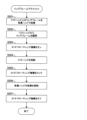
- step S601 of substrate processing in FIG. 11 calibration is performed to determine the plane of the upper surface (back surface) of the semiconductor substrate W to be processed.
- FIG. 13A is a flowchart showing an example of calibration
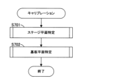
- FIG. 13B is a flowchart showing an example of stage plane identification performed in the calibration of FIG. 13A
- FIG. 13C is a flowchart showing an example of stage plane identification performed in the calibration of FIG. 13A. It is a flowchart which shows a specific example.
- imaging of the suction plate 31 or the semiconductor substrate W is performed as appropriate. In the description here, it is assumed that imaging is performed by the imaging unit 8B. However, even if the imaging unit 8A performs imaging, the following operations can be performed in the same way.
- stage plane identification (FIG. 13B) is performed.
- the count value I for identifying a plurality of (three) imaging points Ps(I) provided on the upper surface 311 of the suction plate 31 of the chuck stage 3 is reset to zero. (step S801), and the count value I is incremented by 1 (step S802).
- the imaging point Ps(I) is, for example, a mark having a predetermined pattern.
- step S803 the control unit 100 adjusts the position of the chuck stage 3 using the XY ⁇ drive table 6 so that the imaging point Ps(I) faces the infrared camera 81 from below. As a result, the imaging point Ps(I) falls within the field of view of the infrared camera 81.
- step S803 the infrared camera 81 images this imaging point Ps(I) to obtain an image indicating the imaging point Ps(I).
- step S804 the control unit 100 checks whether a predetermined pattern possessed by the imaging point Ps(I) can be detected from the image by image processing such as pattern matching.
- the control unit 100 causes the Z-axis camera motor 892 to By driving the camera 81 in the Z direction, the distance of the infrared camera 81 in the Z direction from the imaging point Ps(I) is changed (step S805). As a result, the focus of the infrared camera 81 is changed in the Z direction. Steps S803 to S805 are repeated until the infrared camera 81 focuses on the imaging point Ps(I) and a predetermined pattern is detected ("YES" in step S804).
- step S806 the control unit 100 calculates the position (X, Y, Z) of the imaging point Ps(I) based on a predetermined pattern detected from the image obtained by imaging the imaging point Ps(I). .
- the X and Y coordinates of the imaging point Ps(I) are calculated based on the position of a predetermined pattern included in the image.
- the Z coordinate of the imaging point Ps(I) is calculated based on the position of the infrared camera 81 in the Z direction when the image in which the predetermined pattern can be detected is taken.
- step S807 it is confirmed whether the count value I has reached 2, that is, whether the positions (X, Y, Z) of the two imaging points Ps(1) and Ps(2) have been acquired. If the count value I is less than 2 (“NO” in step S807), the process returns to step S802 and steps S802 to S806 are executed. If the count value I is 2 ("YES" in step S807), the process advances to step S808.
- step S808 a rotation angle ⁇ a for rotating the chuck stage 3 in the ⁇ direction is calculated so that a straight line passing through the two imaging points Ps(1) and Ps(2) becomes horizontal. If the difference between the current rotation angle (actual rotation angle and rotation angle ⁇ a) of the suction plate 31 is not zero (“NO” in step S809), the chuck stage 3 is rotated by the rotation angle ⁇ a. (Step S810), returning to step S801. In this way, steps S801 to S809 are executed.
- step S809 If the difference between the current rotation angle of the suction plate 31 (actual rotation angle and rotation angle ⁇ a) is zero (“YES” in step S809), the process advances to step S811.
- step S811 the control unit 100 images the imaging point Ps(3) with the infrared camera 81 in the same manner as in step S803, and obtains an image showing the imaging point Ps(3). Then, in step S812, the control unit 100 checks whether a predetermined pattern possessed by the imaging point Ps(3) can be detected from the image by image processing such as pattern matching.
- step S812 If the predetermined pattern cannot be detected from the image (“NO” in step S812), the control unit 100 causes the Z-axis camera motor 892 to drive the infrared camera 81 in the Z direction, thereby detecting the imaging point Ps(3). The distance of the infrared camera 81 in the Z direction relative to the target is changed (step S813). Then, steps S811 to S813 are repeated until the predetermined pattern is detected ("YES" in step S812).
- step S812 If the predetermined pattern can be detected in step S812 (YES), the control unit 100 determines the position of the imaging point Ps(3) ( X, Y, Z) are calculated (step S814). As a result, the positions (X, Y, Z) of the three imaging points Ps(1), Ps(2), and Ps(3) are obtained. In step S815, a plane passing through these three positions (X, Y, Z) is specified as the plane of the chuck stage 3, specifically, the plane representing the upper surface 311 of the suction plate 31.
- the semiconductor substrate W is divided into a lattice shape by division lines S (Sa, Sb) that are orthogonal to each other. That is, the semiconductor substrate W is provided with a plurality of parallel dividing lines Sa and a plurality of parallel dividing lines Sb, and the dividing lines Sa and Sb are orthogonal to each other. In this way, a plurality of semiconductor chips C are arranged in a grid pattern with the scheduled dividing lines Sa and Sb in between.
- an area including the intersection of the planned dividing line Sa and the planned dividing line Sb (in other words, a point surrounded by the semiconductor chips C arranged at the four corners) is set as the imaging point Pw(I). .
- the infrared camera 81 detects the division lines Sa, Sb formed on the front surface of the semiconductor substrate W and the semiconductor chips C, and the back surface of the semiconductor substrate W. The image is captured using infrared light.
- step S906 the control unit 100 calculates the position (X, Y, Z) of the imaging point Pw(I) based on a predetermined pattern detected from the image obtained by imaging the imaging point Pw(I). .
- the X and Y coordinates of the imaging point Pw(I) are calculated based on the position of a predetermined pattern included in the image.
- the Z coordinate of the imaging point Pw(I) is calculated based on the position of the infrared camera 81 in the Z direction when the image in which the predetermined pattern can be detected is taken.
- step S908 the rotation angle ⁇ b for rotating the chuck stage 3 in the ⁇ direction is set at two imaging points Pw(1) and Pw( Calculated based on 2). If the difference between the current rotation angle of the suction plate 31 (actual rotation angle and rotation angle ⁇ b) is not zero (“NO” in step S909), the chuck stage 3 is rotated by the rotation angle ⁇ b. (Step S910), returning to step S901. In this way, steps S901 to S909 are executed.
- step S909 If the difference between the current rotation angle of the suction plate 31 (actual rotation angle and rotation angle ⁇ b) is zero (“YES” in step S909), the process advances to step S911.
- step S911 the control unit 100 images the imaging point Pw(3) with the infrared camera 81 in the same manner as in step S903, and obtains an image showing the imaging point Pw(3). Then, in step S912, the control unit 100 checks whether a predetermined pattern possessed by the imaging point Pw(3) can be detected from the image by image processing such as pattern matching.
- the control unit 100 causes the Z-axis camera motor 892 to drive the infrared camera 81 in the Z direction, thereby detecting the imaging point Pw(3).
- the distance of the infrared camera 81 in the Z direction relative to the distance is changed (step S913).
- steps S911 to S913 are repeated until the predetermined pattern is detected ("YES" in step S912).
- the range in which the height of the infrared camera 81 is changed is set based on the stage plane, as described above.
- step S912 If the predetermined pattern can be detected in step S912 (YES), the control unit 100 determines the position of the imaging point Pw(3) ( X, Y, Z) are calculated (step S914). As a result, the positions (X, Y, Z) of the three imaging points Pw(1), Pw(2), and Pw(3) are obtained. In step S915, a plane passing through these three positions (X, Y, Z) is specified as a plane representing the semiconductor substrate W.
- step S602 the line processing process of irradiating the laser beam B to the laser irradiation position Lb while moving the laser irradiation position Lb in the X direction along the target division line Sa is performed to divide the target among the plurality of division lines Sa.
- step S602 processing using the laser beam B is executed on each of the plurality of planned dividing lines Sa.
- the line processing process moves the laser irradiation position Lb to the (+X) side in the X direction
- the line processing process moves the laser irradiation position Lb to the (-X) side in the X direction. Processing is performed alternately.
- the movement of the laser beam B toward the (+X) side with respect to the planned dividing line Sa is performed by driving the chuck stage 3 holding the semiconductor substrate W toward the (-X) side by the X-axis drive unit 65.
- the movement of the laser beam B toward the ( ⁇ X) side with respect to the planned dividing line Sa is executed by driving the chuck stage 3 holding the semiconductor substrate W toward the (+X) side by the X-axis drive unit 65.
- the planned dividing line Sa to be subjected to line processing is changed by driving the chuck stage 3 holding the semiconductor substrate W in the Y direction by the Y-axis drive section 63.
- control unit 100 controls the Z-axis head motor 792 to adjust the position of the processing head 71 in the Z direction based on the plane representing the semiconductor substrate W specified in the calibration in step S601. Thereby, the condensing position of the laser beam B is adjusted inside the semiconductor substrate W, and a modified layer is formed inside the semiconductor substrate W along the planned dividing line Sa.
- step S602 when the line processing for each of the plurality of planned division lines Sa is completed (step S602), the chuck stage 3 holding the semiconductor substrate W is rotated by 90 degrees in the ⁇ direction by the ⁇ -axis table motor 66.
- the plurality of planned dividing lines Sb are positioned parallel to the X direction. 12 (column "S603" in FIG. 12).
- step S604 calibration is performed in the same manner as in step S601 above. Further, in step S605, line processing processing is performed on each of the plurality of scheduled division lines Sb in the same manner as in step S602 described above.
- FIG. 14 is a flowchart showing the basic process of line processing for each dividing line
- FIG. 15A is a diagram schematically showing a first example of the operation performed according to the flowchart of FIG. 14.
- the locus of the laser irradiation position Lb that moves relative to the semiconductor substrate W is shown by a dotted line
- the trajectory is shown along the dividing lines S1, S2, S3 on both sides of the dividing lines S1, S2, S3.
- Virtual straight lines Sv1, Sv2, and Sv3 extending parallel to the X direction between the two are indicated by dashed-dotted lines.
- a dotted line indicating the trajectory of the laser irradiation position Lb is shown preferentially.
- the flowchart in FIG. 14 is started from a state where the laser irradiation position Lb is stopped at a position Pb1 on the (-X) side of the semiconductor substrate W in the X direction.
- This position Pb1 is provided on the virtual straight line Sv1 along the planned dividing line S1, in other words, it is a position facing the planned dividing line S1 from the X direction.
- the position of the laser irradiation position Lb at the time of starting the flowchart in FIG. 14 is not limited to this example, and can be changed as appropriate.
- step S1001 the laser irradiation position Lb, which stops at the position Pb1, starts accelerating toward the (+X) side of the X direction and moves in parallel to the X direction. As a result, the laser irradiation position Lb moves toward the (+X) side along the virtual straight line Sv1. If the speed Vx of the laser irradiation position Lb increases to the processing speed Vxd by the time the laser irradiation position Lb reaches the edge of the semiconductor substrate W on the (-X) side, the laser irradiation position Lb will move in the X direction at the processing speed Vxd. (+X) side at a constant speed (step S1002).
- the laser light source 72 is turned on, and the laser light B is irradiated from the processing head 71 to the laser irradiation position Lb.
- the process is started (step S1003).
- the laser light source 72 is turned off, and the irradiation of the laser light B from the processing head 71 to the laser irradiation position Lb ends. (Step S1004).
- the laser irradiation position Lb moves toward the (+X) side along the division planned line S1, and the laser beam B is irradiated to the laser irradiation position Lb, so that the laser beam B is applied to the division planned line S1.
- Laser processing is performed on the material (line processing).
- the laser irradiation position Lb When the laser irradiation position Lb passes the dividing line S1 in the (+X) side, the laser irradiation position Lb starts decelerating toward the (+X) side in the X direction (step S1005), and the ( The laser irradiation position Lb stops at the position Pb2 on the +X) side (step S1006).
- This position Pb2 is provided on the virtual straight line Sv2 adjacent to the virtual straight line Sv1 in the Y direction, in other words, it is a position facing the planned dividing line S2 from the X direction. That is, in steps S1005 and S1006, the laser irradiation position Lb moves in the Y direction from the virtual straight line Sv1 to the virtual straight line Sv2 in parallel with deceleration in the X direction.
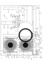
- the positional relationship between the imaging range Ri (FIG. 1) of the imaging units 8A and 8B and the laser irradiation position Lb of the processing head 71 is fixed. Therefore, in steps S1001 to S1006, as the laser irradiation position Lb moves relative to the semiconductor substrate W, the imaging range Ri also moves relative to the semiconductor substrate W.
- the imaging range Ri of the imaging unit 8B is stopped at a position that includes at least the imaging point Pw (S2).
- This imaging point Pw (S2) is an intersection where the scheduled dividing line S2 and the scheduled dividing line S perpendicular thereto intersect in the semiconductor substrate W.
- step S1006 the control unit 100 causes the imaging unit 8B to image the imaging range Ri, and acquires an image including the imaging point Pw (S2). Thereby, the control unit 100 can acquire an image showing the position of the unprocessed planned dividing line S2.
- step S1007 it is confirmed whether laser processing has been completed for a plurality of planned dividing lines S parallel to the X direction. If there is an unprocessed planned dividing line S among these planned dividing lines S (“NO” in step S1007), the process returns to step S1001.
- the laser irradiation position Lb that has passed the planned dividing line S1 to the (+X) side starts deceleration (in other words, the X coordinate where the uniform velocity movement to the (+X) side ends).
- the position at which the laser irradiation position Lb, which accelerates toward the (-X) side toward the planned dividing line S, ends its acceleration is: Match.
- the X coordinate at which the laser irradiation position Lb, which has passed through the planned division line Sn where the line processing is executed on the nth line, finishes moving at a constant velocity and starts decelerating, and the division on which the line processing is executed on the n+1st This coincides with the X direction in which the laser irradiation position Lb toward the scheduled line Sn+1 finishes accelerating and starts moving at a constant speed.
- the laser light source 72 is turned on and the irradiation of the laser light B from the processing head 71 to the laser irradiation position Lb starts. (Step S1003). Further, in accordance with the timing when the laser irradiation position Lb reaches the edge of the semiconductor substrate W on the (-X) side, the laser light source 72 is turned off, and the laser light B is irradiated from the processing head 71 to the laser irradiation position Lb. The process ends (step S1004).
- the laser irradiation position Lb is irradiated with the laser beam B while moving toward the (-X) side along the division planned line S2, and the laser beam B is irradiated on the laser irradiation position Lb.
- Laser processing is performed on (line processing).
- the laser irradiation position Lb When the laser irradiation position Lb passes the planned dividing line S2 in the (-X) side, the laser irradiation position Lb starts decelerating toward the (-X) side in the X direction (step S1005), and the semiconductor substrate W in the X direction starts decelerating.
- the laser irradiation position Lb stops at a position Pb3 on the (-X) side of (step S1006).
- This position Pb3 is provided on the virtual straight line Sv3 adjacent to the virtual straight line Sv2 in the Y direction, in other words, it is a position facing the planned division line S3 from the X direction. That is, in steps S1005 and S1006, the laser irradiation position Lb moves in the Y direction from the virtual straight line Sv2 to the virtual straight line Sv3 in parallel with the deceleration in the X direction.
- the imaging range Ri of the imaging unit 8A is stopped at a position that includes at least the imaging point Pw (S3).
- This imaging point Pw (S3) is an intersection where the scheduled dividing line S3 and the scheduled dividing line S perpendicular thereto intersect in the semiconductor substrate W. Therefore, in step S1006, the control unit 100 causes the imaging unit 8A to image the imaging range Ri, and acquires an image including the imaging point Pw (S3). Thereby, the control unit 100 can acquire an image showing the position of the unprocessed planned division line S3.
- the speed Vx indicates the speed at which the laser irradiation position Lb moves in the X direction with respect to the semiconductor substrate W
- the speed Vy indicates the speed at which the laser irradiation position Lb moves in the Y direction with respect to the semiconductor substrate W.
- the laser irradiation position Lb moves in the Y direction from the virtual straight line Sv1 to the virtual straight line Sv2. That is, in steps S1001 and S1002, the laser irradiation position Lb moves in the Y direction from the virtual straight line Sv1 to the virtual straight line Sv2 in parallel with acceleration in the X direction. As a result, the laser irradiation position Lb reaches the scheduled dividing line S2, and line processing to the scheduled dividing line S2 can be started.
- the laser irradiation position Lb is set at a constant processing speed Vxd. While moving in the X direction, it does not move in the Y direction.
- Step S1005 When the laser irradiation position Lb passes through the planned dividing line S2 in the (-X) side, the laser irradiated position Lb decelerates toward the (-X) side in the X direction.
- Step S1006 the laser irradiation position Lb stops at position Pb3 on the (-X) side of the semiconductor substrate W in the X direction.
- This position Pb3 is provided between the virtual straight line Sv2 and the virtual straight line Sv3 in the Y direction.
- step S1002 to S1004 the laser irradiation position Lb is moved in the X direction at a constant processing speed Vxd. while moving in the Y direction.
- the laser irradiation position Lb continues to move in the Y direction toward the position Pb2 even after the deceleration period Td ends. Further, while the laser irradiation position Lb moves in the Y direction toward the position Pb2 from the end of the deceleration period Td, the laser irradiation position Lb is stopped in the X direction (that is, the speed Vx is zero). Then, at the same time that the laser irradiation position Lb reaches the position Pb2, the acceleration period Ta starts, and the laser irradiation position Lb starts moving in the Y direction from the position Pb2 to the virtual straight line Sv2. Further, at the same time as the acceleration period Ta ends, the laser irradiation position Lb reaches the virtual straight line Sv2.
- FIG. 15G is a diagram schematically showing a seventh example of the operation performed according to the flowchart of FIG. 14.
- the notation in FIG. 15G is similar to that in FIG. 15A.
- laser processing is sequentially performed on the planned division lines S1, S2, and S3 according to the flowchart in FIG. 14.
- the operation during the switching period Tc for changing the scheduled dividing line S to be subjected to laser processing differs between FIG. 15G and FIG. 15A. Therefore, the explanation will focus on the differences from FIG. 15A, and the common operations will be given corresponding symbols and the explanation will be omitted as appropriate.
- step S1002 to S1004 the laser irradiation position Lb is moved in the X direction at a constant processing speed Vxd. while moving in the Y direction.
- the position Pb2 is provided on the opposite side of the virtual straight line Sv1 to the virtual straight line Sv2 in the Y direction.
- the position Pb2 may be provided on the opposite side of the virtual straight line Sv2 to the virtual straight line Sv1 in the Y direction.
- the laser irradiation position Lb moves in the Y direction from the virtual straight line Sv1 to the position Pb2
- the acceleration period Ta the laser irradiation position Lb moves from the position Pb2 beyond the virtual straight line Sv1 to the virtual straight line Sv2. Move in the Y direction. Similar changes can be made to position Pb3.
- Step S1008 in FIG. 16 is executed as follows. That is, the semiconductor substrate W is imaged while the laser irradiation position Lb is moving along the planned dividing line S1 (step S1008). Specifically, the imaging range Ri (i.e., the imaging range Ri of the imaging unit 8A) is located on the moving side (i.e., (+X) side) of the laser irradiation position Lb that moves to the (+X) side. ) is imaged. As a result, an image including an imaging point Pw (S11) on the moving side of the laser irradiation position Lb than the laser irradiation position Lb is acquired. In this way, it is possible to obtain an image showing the position of the unprocessed portion of the scheduled division line S1 on which line processing is being performed.
- the semiconductor substrate W is imaged while the laser irradiation position Lb is moving along the planned dividing line S2 (step S1008).
- the imaging range Ri that is, the imaging section 8B located on the moving side (that is, the (-X) side) of the laser irradiation position Lb that moves to the (-X) side A range Ri) is imaged.
- an image including an imaging point Pw (S21) on the moving side of the laser irradiation position Lb than the laser irradiation position Lb is acquired. In this way, it is possible to obtain an image showing the position of the unprocessed portion of the planned division line S2 on which line processing is currently being performed.
- Steps S1001 to S1007 are then repeated until it is confirmed that the laser processing has been completed for the plurality of scheduled dividing lines S (S1, S2, S3,%) parallel to the X direction ("YES" in step S1007). It will be done.
- FIG. 18 is a flowchart showing a second application example of line processing processing for each scheduled dividing line
- FIG. 19A is a diagram schematically showing a first example of the operation performed according to the flowchart of FIG. 18.
- the locus of the laser irradiation position Lb that moves relative to the semiconductor substrate W is shown by a dotted line
- the trajectory is shown along the dividing lines S1, S2, S3 on both sides of the dividing lines S1, S2, S3.
- Virtual straight lines Sv1, Sv2, and Sv3 extending parallel to the X direction between the two are indicated by dashed-dotted lines.
- a dotted line indicating the trajectory of the laser irradiation position Lb is shown preferentially.
- the flowchart in FIG. 18 is started from a state where the laser irradiation position Lb is stopped at a position Pb1 on the ( ⁇ X) side of the semiconductor substrate W in the X direction.
- This position Pb1 is provided on the virtual straight line Sv1 along the planned dividing line S1, in other words, it is a position facing the planned dividing line S1 from the X direction.
- the position of the laser irradiation position Lb at the time of starting the flowchart of FIG. 18 is not limited to this example, and can be changed as appropriate.
- step S1101 the laser irradiation position Lb, which stops at the position Pb1, starts accelerating toward the (+X) side of the X direction and moves in parallel to the X direction. As a result, the laser irradiation position Lb moves toward the (+X) side along the virtual straight line Sv1. If the speed Vx of the laser irradiation position Lb increases to the processing speed Vxd by the time the laser irradiation position Lb reaches the edge of the semiconductor substrate W on the (-X) side, the laser irradiation position Lb will move in the X direction at the processing speed Vxd. (+X) side at a constant speed (step S1102).
- the semiconductor substrate W is imaged while the laser irradiation position Lb is moving along the planned dividing line S1 (step S1104).
- the imaging range Ri i.e., the imaging range Ri of the imaging unit 8A
- the moving side i.e., (+X) side
- the laser irradiation position Lb that moves to the (+X) side.
- an image including an imaging point Pw (S11) on the moving side of the laser irradiation position Lb than the laser irradiation position Lb is acquired. In this way, it is possible to obtain an image showing the position of the unprocessed portion of the scheduled division line S1 on which line processing is being performed.
- Step S1105 in accordance with the timing when the laser irradiation position Lb reaches the edge of the semiconductor substrate W on the (+X) side, the laser light source 72 is turned off, and the irradiation of the laser light B from the processing head 71 to the laser irradiation position Lb ends.
- Step S1105 in accordance with the timing when the laser irradiation position Lb reaches the edge of the semiconductor substrate W on the (+X) side, the laser light source 72 is turned off, and the irradiation of the laser light B from the processing head 71 to the laser irradiation position Lb ends.
- step S1106 it is confirmed whether laser processing has been completed for a plurality of scheduled division lines S parallel to the X direction. If there is an unprocessed planned dividing line S among these scheduled dividing lines S ("NO" in step S1107), the process returns to step S1101.
- inversion driving is performed in the X direction in the same manner as described above.
- the laser irradiation position Lb moves in the Y direction from the virtual straight line Sv1 to the virtual straight line Sv2.
- the laser irradiation position Lb moves to the virtual straight line Sv2 in the Y direction, and the laser irradiation position Lb reaches the planned dividing line S2. do.
- the manner in which the laser irradiation position Lb moves in the Y direction is different from that described above.
- the laser irradiation position Lb continuously moves in the Y direction from the planned dividing line Sb1 to the scheduled dividing line Sb2.
- Execute (continuous feed drive) In particular, continuous feeding drive of the laser irradiation position Lb in the Y direction is performed before and after the time when the speed Vx of the laser irradiation position Lb in the X direction becomes zero due to the reversal drive. Therefore, in this example, there is no timing when both the velocity Vx in the X direction and the velocity Vy in the Y direction of the laser irradiation position Lb become zero.
- the semiconductor substrate W is imaged while the laser irradiation position Lb is moving along the planned dividing line S2 (step S1104).
- the imaging range Ri i.e., the imaging section 8B's imaging area A range Ri
- an image including an imaging point Pw (S21) on the moving side of the laser irradiation position Lb than the laser irradiation position Lb is acquired. In this way, it is possible to obtain an image showing the position of the unprocessed portion of the scheduled division line S2 on which line processing is being performed.
- step S1105 the unprocessed portion of the scheduled dividing line S2 that is the target of the line processing is An image is captured.
- Step S1101 If the speed Vx of the laser irradiation position Lb increases to the processing speed Vxd by the time the laser irradiation position Lb reaches the edge of the semiconductor substrate W on the (-X) side, the laser irradiation position Lb will move in the X direction at the processing speed Vxd. (+X) side at a constant speed (step S1102).
- the semiconductor substrate W is imaged while the laser irradiation position Lb is moving along the planned dividing line S3 (step S1104).
- the imaging range Ri i.e., the imaging range Ri of the imaging unit 8A located on the moving side (i.e., (+X) side) of the laser irradiation position Lb that moves to the (+X) side
- an image including an imaging point Pw (S31) on the moving side of the laser irradiation position Lb than the laser irradiation position Lb is acquired. In this way, it is possible to obtain an image showing the position of the unprocessed portion of the planned division line S3 on which line processing is currently being performed.
- Step S1105) in accordance with the timing when the laser irradiation position Lb reaches the edge of the semiconductor substrate W on the (+X) side, the laser light source 72 is turned off, and the irradiation of the laser light B from the processing head 71 to the laser irradiation position Lb ends.
- Step S1105 in accordance with the timing when the laser irradiation position Lb reaches the edge of the semiconductor substrate W on the (+X) side, the laser light source 72 is turned off, and the irradiation of the laser light B from the processing head 71 to the laser irradiation position Lb ends.
- step S1103 to S1105 in which a line processing process is executed in which the laser beam B is moved toward the (+X) side along the planned division line S1
- the laser irradiation position Lb is moved in the X direction at a constant processing speed Vxd. while moving in the Y direction.
- the X-axis drive unit 65 (processing axis drive unit) irradiates laser beams that have passed through the scheduled dividing line S1 (first processing line) to the (+X) side (first side) in the X direction (processing direction).
- the laser irradiation position Lb is aligned with the scheduled division line S2 (the first division line S2). 2 processing line).
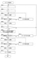
- FIG. 21 is a flowchart showing an example of a method for determining laser processing conditions in line processing
- FIG. 22A is a diagram showing parameters related to determining laser processing conditions
- FIG. 22B is a diagram showing the temporal influence of laser processing conditions
- 22C is a diagram showing an example of a table referred to in determining the laser processing conditions in FIG. 21. This table is stored in the storage unit 190 in advance.
- An irradiation position scan is performed in which the laser irradiation position Lb overlapping the planned division line S is irradiated with the laser beam B while moving the laser irradiation position Lb in the X direction until . That is, in the irradiation position scanning, the laser irradiation position Lb is moved in the X direction from the start point Xs to the end point Xe by the Irradiate light B. In this way, the above-mentioned line processing process is executed along with the scanning of the irradiation position.
- a constant velocity section SC is set for the planned division line S.
- This constant velocity section SC is located between the start point Xs and the end point Xe in the X direction, and is set to include the planned dividing line S.
- both ends of the constant velocity section SC coincide with both ends of the planned dividing line S in the X direction, in other words, the constant velocity section SC coincides with the planned dividing line S.
- the manner in which the constant velocity section SC is set is not limited to this example, and the constant velocity section SC may be set by adding an offset outward from both ends of the planned dividing line S. In this case, the constant velocity section SC is longer than the planned dividing line S.
- the laser irradiation position Lb moves in the X direction from a start point Xs provided on one side of the constant velocity section SC to an end point Xe provided on the other side of the constant velocity section SC.
- the laser irradiation position Lb is accelerated at an acceleration A in the X direction, and the laser irradiation position Lb is The speed Vx in the X direction at the position Lb increases from zero to the processing speed Vxd.
- the laser irradiation position Lb moves from one end Xss to the other end Xse of the constant velocity section SC in the X direction
- the laser The irradiation position Lb moves in the X direction at a constant processing speed Vxd.
- the laser irradiation position Lb decelerates in the X direction at an acceleration A, and the laser irradiation position
- the speed Vx of Lb in the X direction decreases from the machining speed Vxd to zero.
- the laser irradiation position Lb is set with respect to the semiconductor substrate W from the start point Xs on one side of the semiconductor substrate W (workpiece) to the end point Xe on the other side in the X direction (processing direction).
- a laser irradiation position Lb that moves along a target dividing line S (one target line) among a plurality of dividing lines S (processing lines).
- the planned dividing line S is processed (irradiation position scanning).
- a constant velocity section SC including the scheduled division line S (target line) is set between the start point Xs and the end point Xe in the X direction.
- the total period (scanning time t) of the acceleration period Ta, the constant velocity period Tsc, and the deceleration period Td can be suppressed. In this way, in the laser processing technology that processes the planned dividing line S by moving the laser beam B along the scheduled dividing line S of the semiconductor substrate W, it becomes possible to efficiently process the scheduled dividing line S. ing.
- the recording medium 192 corresponds to an example of the "recording medium” of the present invention
- the laser beam B corresponds to an example of the "laser light” of the present invention
- the laser irradiation position Lb corresponds to the "laser irradiation position” of the present invention.
- the scheduled dividing line S corresponds to an example of the "processing line” of the present invention
- the constant velocity section SC corresponds to an example of the "uniform velocity section” of the present invention
- the acceleration period Ta corresponds to an example of the "processing line” of the present invention.
Landscapes
- Physics & Mathematics (AREA)
- Optics & Photonics (AREA)
- Engineering & Computer Science (AREA)
- Plasma & Fusion (AREA)
- Mechanical Engineering (AREA)
- Laser Beam Processing (AREA)
- Dicing (AREA)
Priority Applications (7)
| Application Number | Priority Date | Filing Date | Title |
|---|---|---|---|
| JP2024515755A JP7571345B2 (ja) | 2022-04-18 | 2022-04-18 | レーザ加工装置、レーザ加工方法、レーザ加工プログラム、記録媒体、半導体チップ製造方法および半導体チップ |
| US18/857,213 US20250285888A1 (en) | 2022-04-18 | 2022-04-18 | Laser processing apparatus, laser processing method, laser processing program, recording medium, semiconductor chip manufacturing method and semiconductor chip |
| PCT/JP2022/018063 WO2023203613A1 (ja) | 2022-04-18 | 2022-04-18 | レーザ加工装置、レーザ加工方法、レーザ加工プログラム、記録媒体、半導体チップ製造方法および半導体チップ |
| KR1020247030035A KR102948781B1 (ko) | 2022-04-18 | 2022-04-18 | 레이저 가공 장치, 레이저 가공 방법, 레이저 가공 프로그램, 기록 매체, 반도체 칩 제조 방법, 및 반도체 칩 |
| DE112022006866.3T DE112022006866T5 (de) | 2022-04-18 | 2022-04-18 | Laserbearbeitungsvorrichtung, Laserbearbeitungsverfahren, Laserbearbeitungsprogramm, Aufzeichnungsmedium, Halbleiterchip-Herstellungsverfahren und Halbleiterchip |
| CN202280094648.2A CN118900742A (zh) | 2022-04-18 | 2022-04-18 | 激光加工装置、激光加工方法、激光加工程序、记录介质、半导体芯片制造方法和半导体芯片 |
| TW111122836A TWI840841B (zh) | 2022-04-18 | 2022-06-20 | 雷射加工裝置、雷射加工方法、雷射加工程式、記錄媒體、半導體晶片製造方法及半導體晶片 |
Applications Claiming Priority (1)
| Application Number | Priority Date | Filing Date | Title |
|---|---|---|---|
| PCT/JP2022/018063 WO2023203613A1 (ja) | 2022-04-18 | 2022-04-18 | レーザ加工装置、レーザ加工方法、レーザ加工プログラム、記録媒体、半導体チップ製造方法および半導体チップ |
Publications (1)
| Publication Number | Publication Date |
|---|---|
| WO2023203613A1 true WO2023203613A1 (ja) | 2023-10-26 |
Family
ID=88419404
Family Applications (1)
| Application Number | Title | Priority Date | Filing Date |
|---|---|---|---|
| PCT/JP2022/018063 Ceased WO2023203613A1 (ja) | 2022-04-18 | 2022-04-18 | レーザ加工装置、レーザ加工方法、レーザ加工プログラム、記録媒体、半導体チップ製造方法および半導体チップ |
Country Status (7)
| Country | Link |
|---|---|
| US (1) | US20250285888A1 (https=) |
| JP (1) | JP7571345B2 (https=) |
| KR (1) | KR102948781B1 (https=) |
| CN (1) | CN118900742A (https=) |
| DE (1) | DE112022006866T5 (https=) |
| TW (1) | TWI840841B (https=) |
| WO (1) | WO2023203613A1 (https=) |
Citations (6)
| Publication number | Priority date | Publication date | Assignee | Title |
|---|---|---|---|---|
| JP2000106340A (ja) * | 1997-09-26 | 2000-04-11 | Nikon Corp | 露光装置及び走査露光方法、並びにステージ装置 |
| JP2008042032A (ja) * | 2006-08-08 | 2008-02-21 | Sumitomo Heavy Ind Ltd | ステージ駆動方法及び該方法を用いたレーザ加工装置 |
| JP2009123875A (ja) * | 2007-11-14 | 2009-06-04 | Tokyo Seimitsu Co Ltd | レーザーダイシング方法 |
| JP2012146723A (ja) * | 2011-01-07 | 2012-08-02 | Disco Abrasive Syst Ltd | ダイシング加工装置 |
| JP2012256796A (ja) * | 2011-06-10 | 2012-12-27 | Disco Abrasive Syst Ltd | 分割予定ライン検出方法 |
| JP2018152494A (ja) * | 2017-03-14 | 2018-09-27 | 株式会社ディスコ | レーザー加工装置 |
Family Cites Families (9)
| Publication number | Priority date | Publication date | Assignee | Title |
|---|---|---|---|---|
| JPS5037082B1 (https=) | 1970-12-31 | 1975-11-29 | ||
| JPS5554593U (https=) | 1978-10-06 | 1980-04-12 | ||
| JPS584716U (ja) | 1981-07-02 | 1983-01-12 | 本田技研工業株式会社 | 内燃機関用消音器 |
| IL135139A0 (en) | 1997-09-19 | 2001-05-20 | Nikon Corp | Stage apparatus, scanning type exposure apparatus, and device produced with the same |
| TWI516327B (zh) * | 2012-11-30 | 2016-01-11 | Lts有限公司 | 用於控制雷射圖案成形裝置之階段的方法 |
| JP2018120913A (ja) * | 2017-01-24 | 2018-08-02 | 株式会社ディスコ | レーザー加工装置 |
| JP7313128B2 (ja) * | 2018-10-04 | 2023-07-24 | 浜松ホトニクス株式会社 | 撮像装置、レーザ加工装置、及び、撮像方法 |
| JP7644328B2 (ja) * | 2020-07-14 | 2025-03-12 | 株式会社東京精密 | レーザ加工装置、ウェーハ加工システム及びレーザ加工装置の制御方法 |
| JP7487045B2 (ja) * | 2020-08-20 | 2024-05-20 | 浜松ホトニクス株式会社 | レーザ加工装置 |
-
2022
- 2022-04-18 US US18/857,213 patent/US20250285888A1/en active Pending
- 2022-04-18 CN CN202280094648.2A patent/CN118900742A/zh active Pending
- 2022-04-18 DE DE112022006866.3T patent/DE112022006866T5/de active Pending
- 2022-04-18 WO PCT/JP2022/018063 patent/WO2023203613A1/ja not_active Ceased
- 2022-04-18 KR KR1020247030035A patent/KR102948781B1/ko active Active
- 2022-04-18 JP JP2024515755A patent/JP7571345B2/ja active Active
- 2022-06-20 TW TW111122836A patent/TWI840841B/zh active
Patent Citations (6)
| Publication number | Priority date | Publication date | Assignee | Title |
|---|---|---|---|---|
| JP2000106340A (ja) * | 1997-09-26 | 2000-04-11 | Nikon Corp | 露光装置及び走査露光方法、並びにステージ装置 |
| JP2008042032A (ja) * | 2006-08-08 | 2008-02-21 | Sumitomo Heavy Ind Ltd | ステージ駆動方法及び該方法を用いたレーザ加工装置 |
| JP2009123875A (ja) * | 2007-11-14 | 2009-06-04 | Tokyo Seimitsu Co Ltd | レーザーダイシング方法 |
| JP2012146723A (ja) * | 2011-01-07 | 2012-08-02 | Disco Abrasive Syst Ltd | ダイシング加工装置 |
| JP2012256796A (ja) * | 2011-06-10 | 2012-12-27 | Disco Abrasive Syst Ltd | 分割予定ライン検出方法 |
| JP2018152494A (ja) * | 2017-03-14 | 2018-09-27 | 株式会社ディスコ | レーザー加工装置 |
Also Published As
| Publication number | Publication date |
|---|---|
| TWI840841B (zh) | 2024-05-01 |
| TW202342215A (zh) | 2023-11-01 |
| KR20240148879A (ko) | 2024-10-11 |
| JP7571345B2 (ja) | 2024-10-22 |
| DE112022006866T5 (de) | 2025-02-20 |
| CN118900742A (zh) | 2024-11-05 |
| US20250285888A1 (en) | 2025-09-11 |
| KR102948781B1 (ko) | 2026-04-06 |
| JPWO2023203613A1 (https=) | 2023-10-26 |
Similar Documents
| Publication | Publication Date | Title |
|---|---|---|
| JP5785418B2 (ja) | 供給装置及び供給方法、画像形成装置 | |
| US11062925B2 (en) | Semiconductor manufacturing apparatus and method of manufacturing semiconductor device | |
| CN101456222A (zh) | 晶片的分割方法 | |
| JP2014179560A (ja) | 斜め認識カメラ及びダイボンダ | |
| JP7571345B2 (ja) | レーザ加工装置、レーザ加工方法、レーザ加工プログラム、記録媒体、半導体チップ製造方法および半導体チップ | |
| WO2023203612A1 (ja) | レーザ加工装置、レーザ加工方法、レーザ加工プログラム、記録媒体、半導体チップ製造方法および半導体チップ | |
| JP7614450B2 (ja) | レーザ加工装置、レーザ加工方法、レーザ加工プログラム、記録媒体、半導体チップ製造方法および半導体チップ | |
| JP7614451B2 (ja) | レーザ加工装置、レーザ加工方法、レーザ加工プログラム、記録媒体、半導体チップ製造方法および半導体チップ | |
| TWI782142B (zh) | 晶圓加工方法 | |
| KR102804197B1 (ko) | 레이저 가공 장치 | |
| JP2020021917A (ja) | ウエーハの加工方法 | |
| JP2007227703A (ja) | 基板分割方法、基板分割装置、電気光学装置、電子機器 | |
| JP2019118949A (ja) | 加工装置 | |
| JP2008103225A (ja) | 試料作製装置及び試料作製方法 | |
| JP2019121624A (ja) | 加工装置 | |
| JP7032147B2 (ja) | 加工装置 | |
| JP2019197784A (ja) | レーザー加工装置 | |
| CN119943758A (zh) | 晶片的加工方法 |
Legal Events
| Date | Code | Title | Description |
|---|---|---|---|
| 121 | Ep: the epo has been informed by wipo that ep was designated in this application |
Ref document number: 22938416 Country of ref document: EP Kind code of ref document: A1 |
|
| ENP | Entry into the national phase |
Ref document number: 2024515755 Country of ref document: JP Kind code of ref document: A |
|
| ENP | Entry into the national phase |
Ref document number: 20247030035 Country of ref document: KR Kind code of ref document: A |
|
| WWE | Wipo information: entry into national phase |
Ref document number: 1020247030035 Country of ref document: KR |
|
| WWE | Wipo information: entry into national phase |
Ref document number: 202280094648.2 Country of ref document: CN |
|
| WWE | Wipo information: entry into national phase |
Ref document number: 18857213 Country of ref document: US |
|
| WWE | Wipo information: entry into national phase |
Ref document number: 112022006866 Country of ref document: DE |
|
| WWP | Wipo information: published in national office |
Ref document number: 112022006866 Country of ref document: DE |
|
| 122 | Ep: pct application non-entry in european phase |
Ref document number: 22938416 Country of ref document: EP Kind code of ref document: A1 |
|
| WWP | Wipo information: published in national office |
Ref document number: 18857213 Country of ref document: US |