WO2023189082A1 - 半導体装置 - Google Patents
半導体装置 Download PDFInfo
- Publication number
- WO2023189082A1 WO2023189082A1 PCT/JP2023/006838 JP2023006838W WO2023189082A1 WO 2023189082 A1 WO2023189082 A1 WO 2023189082A1 JP 2023006838 W JP2023006838 W JP 2023006838W WO 2023189082 A1 WO2023189082 A1 WO 2023189082A1
- Authority
- WO
- WIPO (PCT)
- Prior art keywords
- insulating layer
- drain electrode
- field plate
- sidewall
- elevation angle
- Prior art date
- Legal status (The legal status is an assumption and is not a legal conclusion. Google has not performed a legal analysis and makes no representation as to the accuracy of the status listed.)
- Ceased
Links
Images


Classifications
-
- H—ELECTRICITY
- H10—SEMICONDUCTOR DEVICES; ELECTRIC SOLID-STATE DEVICES NOT OTHERWISE PROVIDED FOR
- H10D—INORGANIC ELECTRIC SEMICONDUCTOR DEVICES
- H10D30/00—Field-effect transistors [FET]
- H10D30/60—Insulated-gate field-effect transistors [IGFET]
- H10D30/67—Thin-film transistors [TFT]
- H10D30/674—Thin-film transistors [TFT] characterised by the active materials
- H10D30/675—Group III-V materials, Group II-VI materials, Group IV-VI materials, selenium or tellurium
-
- H—ELECTRICITY
- H10—SEMICONDUCTOR DEVICES; ELECTRIC SOLID-STATE DEVICES NOT OTHERWISE PROVIDED FOR
- H10D—INORGANIC ELECTRIC SEMICONDUCTOR DEVICES
- H10D30/00—Field-effect transistors [FET]
- H10D30/40—FETs having zero-dimensional [0D], one-dimensional [1D] or two-dimensional [2D] charge carrier gas channels
- H10D30/47—FETs having zero-dimensional [0D], one-dimensional [1D] or two-dimensional [2D] charge carrier gas channels having two-dimensional [2D] charge carrier gas channels, e.g. nanoribbon FETs or high electron mobility transistors [HEMT]
- H10D30/471—High electron mobility transistors [HEMT] or high hole mobility transistors [HHMT]
- H10D30/475—High electron mobility transistors [HEMT] or high hole mobility transistors [HHMT] having wider bandgap layer formed on top of lower bandgap active layer, e.g. undoped barrier HEMTs such as i-AlGaN/GaN HEMTs
- H10D30/4755—High electron mobility transistors [HEMT] or high hole mobility transistors [HHMT] having wider bandgap layer formed on top of lower bandgap active layer, e.g. undoped barrier HEMTs such as i-AlGaN/GaN HEMTs having wide bandgap charge-carrier supplying layers, e.g. modulation doped HEMTs such as n-AlGaAs/GaAs HEMTs
-
- H—ELECTRICITY
- H10—SEMICONDUCTOR DEVICES; ELECTRIC SOLID-STATE DEVICES NOT OTHERWISE PROVIDED FOR
- H10D—INORGANIC ELECTRIC SEMICONDUCTOR DEVICES
- H10D30/00—Field-effect transistors [FET]
- H10D30/01—Manufacture or treatment
- H10D30/015—Manufacture or treatment of FETs having heterojunction interface channels or heterojunction gate electrodes, e.g. HEMT
-
- H—ELECTRICITY
- H10—SEMICONDUCTOR DEVICES; ELECTRIC SOLID-STATE DEVICES NOT OTHERWISE PROVIDED FOR
- H10D—INORGANIC ELECTRIC SEMICONDUCTOR DEVICES
- H10D30/00—Field-effect transistors [FET]
- H10D30/40—FETs having zero-dimensional [0D], one-dimensional [1D] or two-dimensional [2D] charge carrier gas channels
- H10D30/47—FETs having zero-dimensional [0D], one-dimensional [1D] or two-dimensional [2D] charge carrier gas channels having two-dimensional [2D] charge carrier gas channels, e.g. nanoribbon FETs or high electron mobility transistors [HEMT]
- H10D30/471—High electron mobility transistors [HEMT] or high hole mobility transistors [HHMT]
- H10D30/475—High electron mobility transistors [HEMT] or high hole mobility transistors [HHMT] having wider bandgap layer formed on top of lower bandgap active layer, e.g. undoped barrier HEMTs such as i-AlGaN/GaN HEMTs
-
- H—ELECTRICITY
- H10—SEMICONDUCTOR DEVICES; ELECTRIC SOLID-STATE DEVICES NOT OTHERWISE PROVIDED FOR
- H10D—INORGANIC ELECTRIC SEMICONDUCTOR DEVICES
- H10D30/00—Field-effect transistors [FET]
- H10D30/60—Insulated-gate field-effect transistors [IGFET]
- H10D30/67—Thin-film transistors [TFT]
- H10D30/6729—Thin-film transistors [TFT] characterised by the electrodes
- H10D30/6737—Thin-film transistors [TFT] characterised by the electrodes characterised by the electrode materials
- H10D30/6738—Schottky barrier electrodes
-
- H—ELECTRICITY
- H10—SEMICONDUCTOR DEVICES; ELECTRIC SOLID-STATE DEVICES NOT OTHERWISE PROVIDED FOR
- H10D—INORGANIC ELECTRIC SEMICONDUCTOR DEVICES
- H10D62/00—Semiconductor bodies, or regions thereof, of devices having potential barriers
- H10D62/80—Semiconductor bodies, or regions thereof, of devices having potential barriers characterised by the materials
- H10D62/85—Semiconductor bodies, or regions thereof, of devices having potential barriers characterised by the materials being Group III-V materials, e.g. GaAs
-
- H—ELECTRICITY
- H10—SEMICONDUCTOR DEVICES; ELECTRIC SOLID-STATE DEVICES NOT OTHERWISE PROVIDED FOR
- H10D—INORGANIC ELECTRIC SEMICONDUCTOR DEVICES
- H10D64/00—Electrodes of devices having potential barriers
- H10D64/01—Manufacture or treatment
- H10D64/011—Manufacture or treatment of electrodes ohmically coupled to a semiconductor
-
- H—ELECTRICITY
- H10—SEMICONDUCTOR DEVICES; ELECTRIC SOLID-STATE DEVICES NOT OTHERWISE PROVIDED FOR
- H10D—INORGANIC ELECTRIC SEMICONDUCTOR DEVICES
- H10D64/00—Electrodes of devices having potential barriers
- H10D64/01—Manufacture or treatment
- H10D64/018—Spacers formed inside holes at the prospective gate locations, e.g. holes left by removing dummy gates
-
- H—ELECTRICITY
- H10—SEMICONDUCTOR DEVICES; ELECTRIC SOLID-STATE DEVICES NOT OTHERWISE PROVIDED FOR
- H10D—INORGANIC ELECTRIC SEMICONDUCTOR DEVICES
- H10D64/00—Electrodes of devices having potential barriers
- H10D64/111—Field plates
- H10D64/112—Field plates comprising multiple field plate segments
-
- H—ELECTRICITY
- H10—SEMICONDUCTOR DEVICES; ELECTRIC SOLID-STATE DEVICES NOT OTHERWISE PROVIDED FOR
- H10D—INORGANIC ELECTRIC SEMICONDUCTOR DEVICES
- H10D64/00—Electrodes of devices having potential barriers
- H10D64/20—Electrodes characterised by their shapes, relative sizes or dispositions
- H10D64/27—Electrodes not carrying the current to be rectified, amplified, oscillated or switched, e.g. gates
- H10D64/311—Gate electrodes for field-effect devices
- H10D64/411—Gate electrodes for field-effect devices for FETs
-
- H—ELECTRICITY
- H10—SEMICONDUCTOR DEVICES; ELECTRIC SOLID-STATE DEVICES NOT OTHERWISE PROVIDED FOR
- H10W—GENERIC PACKAGES, INTERCONNECTIONS, CONNECTORS OR OTHER CONSTRUCTIONAL DETAILS OF DEVICES COVERED BY CLASS H10
- H10W74/00—Encapsulations, e.g. protective coatings
- H10W74/10—Encapsulations, e.g. protective coatings characterised by their shape or disposition
- H10W74/131—Encapsulations, e.g. protective coatings characterised by their shape or disposition the semiconductor body being only partially enclosed
- H10W74/147—Encapsulations, e.g. protective coatings characterised by their shape or disposition the semiconductor body being only partially enclosed the encapsulations being multilayered
-
- H—ELECTRICITY
- H10—SEMICONDUCTOR DEVICES; ELECTRIC SOLID-STATE DEVICES NOT OTHERWISE PROVIDED FOR
- H10D—INORGANIC ELECTRIC SEMICONDUCTOR DEVICES
- H10D62/00—Semiconductor bodies, or regions thereof, of devices having potential barriers
- H10D62/80—Semiconductor bodies, or regions thereof, of devices having potential barriers characterised by the materials
- H10D62/85—Semiconductor bodies, or regions thereof, of devices having potential barriers characterised by the materials being Group III-V materials, e.g. GaAs
- H10D62/8503—Nitride Group III-V materials, e.g. AlN or GaN
-
- H—ELECTRICITY
- H10—SEMICONDUCTOR DEVICES; ELECTRIC SOLID-STATE DEVICES NOT OTHERWISE PROVIDED FOR
- H10D—INORGANIC ELECTRIC SEMICONDUCTOR DEVICES
- H10D64/00—Electrodes of devices having potential barriers
- H10D64/111—Field plates
-
- H—ELECTRICITY
- H10—SEMICONDUCTOR DEVICES; ELECTRIC SOLID-STATE DEVICES NOT OTHERWISE PROVIDED FOR
- H10D—INORGANIC ELECTRIC SEMICONDUCTOR DEVICES
- H10D64/00—Electrodes of devices having potential barriers
- H10D64/60—Electrodes characterised by their materials
- H10D64/64—Electrodes comprising a Schottky barrier to a semiconductor
Definitions
- the present disclosure relates to a semiconductor device, and particularly relates to a group III nitride semiconductor device using a group III nitride semiconductor.
- a group III nitride semiconductor device using a group III nitride semiconductor, particularly gallium nitride (GaN) or aluminum gallium nitride (AlGaN), has a high dielectric breakdown voltage due to the wide band gap of the material. Further, in a group III nitride semiconductor device, a heterostructure such as AlGaN/GaN can be easily formed.
- a high concentration of electrons (hereinafter referred to as "two-dimensional electron gas") is generated on the GaN layer side of the AlGaN/GaN interface due to the piezoelectric polarization generated from the lattice constant difference between the materials and the spontaneous polarization of AlGaN and GaN. ) is formed.
- Group III nitride semiconductor devices that utilize this two-dimensional electron gas channel have a relatively high electron saturation velocity, relatively high insulation resistance, and relatively high thermal conductivity, so they are suitable for high-frequency power devices. It is applied.
- Lg the gate dimension
- FIG. 19 is a cross-sectional view showing the configuration of a gate electrode 140x of the prior art. Specifically, FIG. 19 shows a structure near a gate electrode 140x in a semiconductor device 100x made of a group III nitride described in Patent Document 1.
- a GaN layer 103x and an AlGaN layer 104x are provided in this order, and a two-dimensional electron gas 110x is generated on the GaN layer 103x side due to the heterostructure. do.
- An insulating layer 130x is provided on the AlGaN layer 104x, and an opening 130Ax is provided in the insulating layer 130x so that the AlGaN layer 104x is exposed.
- a first sidewall 133dx on the drain electrode side and a second sidewall 133sx on the source electrode side are provided in the opening 130Ax so as to be in contact with the side surface of the insulating layer 130x.
- the drain electrode is placed on the positive side of the X-axis rather than the gate electrode 140x, and the source electrode is placed on the negative side of the X-axis than the gate electrode 140x. There is.
- the drain electrode and the source electrode are each ohmically connected to the two-dimensional electron gas 110x.
- the gate electrode 140x is provided so as to cover the insulating layer 130x and the opening 130Ax so as to have a so-called T-shaped cross section (T-shaped gate structure).
- Patent Document 1 describes that Lg can be reduced from about 0.1 ⁇ m to about 0.3 ⁇ m by using a T-type gate structure.
- the parasitic capacitance between the gate electrode 140x and the drain electrode can be reduced by the insulating layer 130x sandwiched between the T-shaped gate electrode 140x and the AlGaN layer 104x.
- electric field relaxation is insufficient.
- a high electric field tends to be locally concentrated at the end of the portion of the gate electrode 140x that extends over the insulating layer 130x on the drain electrode side.
- the first problem is that electric field relaxation and parasitic capacitance reduction cannot be achieved at the same time.
- the electron density of the two-dimensional electron gas 110x becomes high directly below the insulating layer 130x and the sidewalls 133dx and 133sx, so that the on-resistance can be lowered.
- the off-state characteristics deteriorate. Specifically, when the transistor is off, the electric field generated directly below the gate electrode 140x becomes weaker, making it difficult for the depletion layer to expand, making it easier to generate off-leakage current between the source and drain. As described above, there is a second problem in that it is not possible to simultaneously lower the on-resistance and improve the off-resistance.
- the present disclosure provides a semiconductor device that can achieve at least one of (i) both electric field relaxation and reduced parasitic capacitance, or (ii) both lower on-resistance and improved off-resistance.
- the purpose is to
- one embodiment of a semiconductor device includes a substrate, a channel layer made of a group III nitride semiconductor provided above the substrate, and a channel layer provided above the channel layer. , a barrier layer made of a group III nitride semiconductor having a larger band gap than the channel layer, and a source electrode and a drain provided above the barrier layer and spaced apart from each other in a first direction in a plan view of the substrate. an electrode, a gate electrode provided with a space between the source electrode and the drain electrode in the first direction, and between the gate electrode and the source electrode and the drain electrode.
- the insulating layer having a first insulating layer made of silicon nitride as a lowermost layer, and a first insulating layer made of silicon oxide above the first insulating layer.
- the gate electrode has a Schottky junction with the barrier layer, and extends in the first direction from the junction to the source electrode side and the drain electrode side, respectively.
- an overhanging portion the insulating layer includes an insulating layer between the overhanging portion and the barrier layer in a second direction perpendicular to the main surface of the substrate, and between the bonding portion and the drain electrode.
- the projecting portion is configured to generate a first electric field in a section from a first position, which is an end of the first sidewall on the side of the joint part, to a second position, which is an end of the first sidewall on the side of the drain electrode, in a plan view.
- a plate, and a second electric field plate in a section from the second position to a third position that is the drain electrode side end of the projecting portion in plan view, and the second electric field plate and the barrier layer are connected to each other.
- the first insulating layer and the second insulating layer are provided therebetween, and in a cross section parallel to each of the first direction and the second direction and passing through the joint portion, the first insulating layer and the second insulating layer are stacked.
- a tangent to the upper surface of the first sidewall at the first position has an inclination of a first elevation angle with respect to the main surface, and the highest position of the lower surface of the first electric field plate is on the main surface when viewed from the first position.
- the drain electrode side end at the lowest position on the lower surface of the second electric field plate has a third elevation angle with respect to the main surface when viewed from the first position;
- the second elevation angle is greater than the third elevation angle, and the lower surface of the second electric field plate includes an inclined surface whose distance from the barrier layer increases monotonically in a direction from the gate electrode to the drain electrode.
- Another aspect of the semiconductor device includes a substrate, a channel layer made of a group III nitride semiconductor provided above the substrate, and a channel layer provided above the channel layer.
- the insulating layer having a first insulating layer made of silicon nitride as the lowermost layer, and a second insulating layer made of silicon oxide above the first insulating layer.
- the gate electrode includes a Schottky junction with the barrier layer, and an overhanging portion that extends from the junction toward the source electrode side and the drain electrode side in the first direction.
- the insulating layer includes a bond between the overhang portion and the barrier layer in a second direction perpendicular to the main surface of the substrate, and between the bonding portion and the drain electrode.
- a first electric field plate in a section from a first position, which is the end of the first sidewall on the side of the joint part, to a second position, which is the end of the first sidewall on the side of the drain electrode, in a plan view; a second electric field plate in a section from the second position to a third position which is the end of the projecting portion on the drain electrode side in a plan view, and between the second electric field plate and the barrier layer;
- the first insulating layer and the second insulating layer are stacked, and in a cross section parallel to each of the first direction and the second direction and passing through the joint, the first sidewall A tangent to the top surface at the first position has an inclination at a first elevation angle with respect to the main surface, and the highest position of the bottom surface of the first electric field plate is at
- the drain electrode side end at the lowest position of the lower surface of the second electric field plate has a third elevation angle relative to the main surface when viewed from the first position, and the first sidewall
- the highest position of the upper surface is located below the highest position of the upper surface of the second sidewall.
- the semiconductor device it is possible to achieve at least one of (i) both electric field relaxation and parasitic capacitance reduction, or (ii) both lower on-resistance and improved off-resistance.
- FIG. 1 is a cross-sectional view showing the configuration of a semiconductor device according to the first embodiment.
- FIG. 2 is an enlarged cross-sectional view showing the structure of the gate electrode of the semiconductor device according to the first embodiment.
- FIG. 3 is an enlarged cross-sectional view for explaining the shape of the lower surface of the protruding portion on the drain electrode side of the gate electrode of the semiconductor device according to the first embodiment.
- FIG. 4A is a cross-sectional view showing each step of the method for manufacturing a semiconductor device according to the first embodiment.
- FIG. 4B is a cross-sectional view showing each step of the method for manufacturing a semiconductor device according to the first embodiment.
- FIG. 4C is a cross-sectional view showing each step of the method for manufacturing a semiconductor device according to the first embodiment.
- FIG. 4D is a cross-sectional view showing each step of the method for manufacturing a semiconductor device according to the first embodiment.
- FIG. 4E is a cross-sectional view showing each step of the method for manufacturing a semiconductor device according to the first embodiment.
- FIG. 4F is a cross-sectional view showing each step of the method for manufacturing a semiconductor device according to the first embodiment.
- FIG. 4G is a cross-sectional view showing each step of the method for manufacturing a semiconductor device according to the first embodiment.
- FIG. 5 is a cross-sectional view showing the configuration of a gate electrode of a semiconductor device according to Modification 1 of Embodiment 1.
- FIG. 6 is an enlarged sectional view for explaining the shape of the lower surface of the protruding portion on the drain electrode side of the gate electrode of the semiconductor device according to Modification 1 of Embodiment 1.
- FIG. 7 is a cross-sectional view showing the structure of a gate electrode of a semiconductor device according to a second modification of the first embodiment.
- FIG. 8 is an enlarged cross-sectional view for explaining the shape of the lower surface of the protruding portion on the drain electrode side of the gate electrode of the semiconductor device according to the second modification of the first embodiment.
- FIG. 9 is an enlarged cross-sectional view for explaining the positional relationship between the shape of the lower surface of the gate electrode and the source field plate of the semiconductor device according to the third modification of the first embodiment.
- FIG. 10 is a cross-sectional view showing the structure of the gate electrode of the semiconductor device according to the second embodiment.
- FIG. 11 is an enlarged cross-sectional view for explaining the shape of the sidewall of the semiconductor device according to the second embodiment.
- FIG. 12 is an enlarged cross-sectional view for explaining the shape of the lower surface of the protruding portion on the drain electrode side of the gate electrode of the semiconductor device according to the second embodiment.
- FIG. 13A is a cross-sectional view showing each step of the method for manufacturing a semiconductor device according to the second embodiment.
- FIG. 13B is a cross-sectional view showing each step of the method for manufacturing a semiconductor device according to the second embodiment.
- FIG. 13C is a cross-sectional view showing each step of the method for manufacturing a semiconductor device according to the second embodiment.
- FIG. 13D is a cross-sectional view showing each step of the method for manufacturing a semiconductor device according to the second embodiment.
- FIG. 13E is a cross-sectional view showing each step of the method for manufacturing a semiconductor device according to the second embodiment.
- FIG. 14 is an enlarged cross-sectional view for explaining the shape of the sidewall of the semiconductor device according to the first modification of the second embodiment.
- FIG. 15 is an enlarged cross-sectional view for explaining the shape of a sidewall of a semiconductor device according to a second modification of the second embodiment.
- FIG. 16 is an enlarged sectional view for explaining the shape of a sidewall of a semiconductor device according to a third modification of the second embodiment.
- FIG. 17 is an enlarged cross-sectional view for explaining the shape of a sidewall of a semiconductor device according to a fourth modification of the second embodiment.
- FIG. 18 is an enlarged sectional view for explaining the shape of a sidewall of a semiconductor device according to a fifth modification of the second embodiment.
- FIG. 19 is a cross-sectional view showing the structure of a conventional gate electrode.
- each figure is a schematic diagram and is not necessarily strictly illustrated.
- substantially the same configurations are denoted by the same reference numerals, and overlapping explanations will be omitted or simplified.
- the terms “upper” and “lower” in the configuration of a semiconductor device do not refer to the upper direction (vertically upward) or the downward direction (vertically downward) in absolute spatial recognition, but rather to the stacked structure. This is a term defined by the relative positional relationship based on the stacking order in . Additionally, the terms “above” and “below” are used not only when two components are spaced apart and there is another component between them; This also applies when two components are placed in close contact with each other.
- the X-axis, Y-axis, and Z-axis indicate three axes of a three-dimensional orthogonal coordinate system.
- two axes parallel to the main surface (top surface) of a substrate included in a semiconductor device are defined as an X-axis and a Y-axis
- a direction perpendicular to the main surface is defined as a Z-axis direction.
- the direction in which the source electrode, gate electrode, and drain electrode are lined up in this order, that is, the so-called gate length direction is set as the X-axis direction.
- the X-axis direction is an example of the first direction.
- the Z-axis direction is an example of the second direction.
- the Z-axis positive direction may be described as “upward” and the Z-axis negative direction may be described as “downward.”
- planar view refers to the main surface (upper surface) of the substrate of the semiconductor device viewed from the positive direction of the Z-axis.
- a group III nitride semiconductor is a semiconductor containing one or more types of group III elements and nitrogen.
- group III elements include aluminum (Al), gallium (Ga), and indium (In).
- group III nitride semiconductors include GaN, AlN, InN, AlGaN, InGaN, and AlInGaN.
- the Group III nitride semiconductor may contain one or more types of elements other than Group III, such as silicon (Si) and phosphorus (P).
- Si silicon
- P phosphorus
- a layer made of a group III nitride semiconductor and a layer composed of a group III nitride semiconductor mean that the layer substantially contains only a group III nitride semiconductor.
- the layer may contain other elements as impurities, such as elements that cannot be avoided during manufacturing, at a rate of 1 at % or less.
- the composition ratio (composition ratio) of group III elements of a nitride semiconductor refers to atoms of a target group III element among a plurality of group III elements contained in the nitride semiconductor. It represents the ratio of numbers.
- the Al composition ratio of the nitride semiconductor layer is a/(a+b+c ) can be expressed as
- the In composition ratio and the Ga composition ratio are represented by b/(a+b+c) and c/(a+b+c), respectively.
- ordinal numbers such as “first” and “second” do not mean the number or order of components, unless otherwise specified, and do not mean the number or order of components. It is used for the purpose of
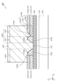
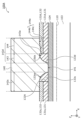
- FIG. 1 is a cross-sectional view showing the configuration of a semiconductor device 100 according to the first embodiment.
- FIG. 2 is an enlarged cross-sectional view showing the configuration of gate electrode 140 of semiconductor device 100 according to the first embodiment.
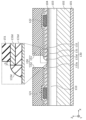
- FIG. 3 is an enlarged cross-sectional view for explaining the shape of the lower surface 144a of the projecting portion 142d on the drain electrode 122 side of the gate electrode 140 of the semiconductor device 100 according to the first embodiment. Note that FIGS.
- the semiconductor device 100 is a high electron mobility transistor (HEMT) having a Schottky junction gate structure.
- HEMT high electron mobility transistor
- the semiconductor device 100 includes a substrate 101, a buffer layer 102, a channel layer 103, a barrier layer 104, a two-dimensional electron gas 110, a source electrode 121, a drain electrode 122, and a source field. It includes a plate 123, a T-shaped gate electrode 140, an insulating layer 130, and a fourth insulating layer 134.
- the insulating layer 130 includes a first insulating layer 131, a second insulating layer 132, a first sidewall 133d, and a second sidewall 133s.
- the substrate 101 is, for example, a substrate made of Si.
- the substrate 101 is not limited to a substrate made of Si, but may be a substrate made of sapphire, SiC, GaN, AlN, or the like.
- the buffer layer 102 is provided above the substrate 101.
- the buffer layer 102 is provided in contact with the upper surface of the substrate 101.
- the buffer layer 102 is, for example, a layer made of a group III nitride semiconductor.
- the buffer layer 102 is composed of a plurality of stacked layers of AlN and AlGaN with a thickness of 2 ⁇ m.
- the buffer layer 102 may be composed of a single layer or multiple layers of a group III nitride semiconductor such as GaN, AlGaN, AlN, InGaN, and AlInGaN.
- the buffer layer 102 may not be provided.
- the channel layer 103 is provided above the substrate 101.
- the channel layer 103 is provided in contact with the upper surface of the buffer layer 102.
- Channel layer 103 is a layer made of a group III nitride semiconductor.
- the channel layer 103 is made of GaN with a thickness of 200 nm, for example.
- the channel layer 103 is not limited to GaN, and may be made of a group III nitride semiconductor such as InGaN, AlGaN, and AlInGaN.
- the channel layer 103 may contain an n-type impurity.
- the thickness of the channel layer 103 is not limited to the example described above.
- the barrier layer 104 is provided above the channel layer 103.
- the barrier layer 104 is provided in contact with the upper surface of the channel layer 103.
- the barrier layer 104 is a layer made of a group III nitride semiconductor having a larger band gap than the channel layer 103.
- the barrier layer 104 is made of, for example, AlGaN with a thickness of 20 nm and an Al composition ratio of 25%.
- a highly concentrated two-dimensional electron gas 110 is generated on the channel layer 103 side of the hetero interface between the barrier layer 104 and the channel layer 103.
- the two-dimensional electron gas 110 is used as a channel of a transistor.
- the barrier layer 104 is not limited to AlGaN, but may be made of a group III nitride semiconductor such as AlInGaN. Further, the barrier layer 104 may contain an n-type impurity. The thickness and Al composition ratio of the barrier layer 104 are not limited to the above example.
- a cap layer made of, for example, GaN and having a thickness of about 1 nm or more and about 2 nm or less may be provided on the barrier layer 104.
- a spacer layer made of, for example, AlN and having a thickness of about 1 nm may be provided between the channel layer 103 and the barrier layer 104 as a spacer layer. In this way, the channel layer 103 and the barrier layer 104 do not need to be in contact with each other.
- the source electrode 121 and the drain electrode 122 are provided above the barrier layer 104 with a space between them. Specifically, the source electrode 121 and the drain electrode 122 are provided to face each other with the gate electrode 140 interposed therebetween.
- the source electrode 121 and the drain electrode 122 are formed using a conductive material.
- the source electrode 121 and the drain electrode 122 are multilayer electrode films having a laminated structure in which a Ti film and an Al film are sequentially laminated, but the invention is not limited thereto.
- the source electrode 121 and the drain electrode 122 are not limited to a stacked structure of a Ti film and an Al film, but may be a transition metal, a transition metal nitride, or a carbide formed by sputtering.
- the source electrode 121 and the drain electrode 122 may be made of Ta, Hf, W, Ni, TiN, TaN, HfN, WN, TiC, TaC, HfC, Au, Cu, etc., or a compound containing these elements.
- it may be a multilayer electrode film consisting of a plurality of laminated structures.
- the source electrode 121 and the drain electrode 122 are electrically ohmically connected to the two-dimensional electron gas 110.
- the source electrode 121 and the drain electrode 122 there is a recessed portion where a part of the barrier layer 104 and/or the channel layer 103 is removed, or an n-type impurity containing a donor such as Si is formed.
- a contact layer containing the contact layer may be provided.
- the contact layer containing n-type impurities may be formed by, for example, plasma treatment, ion implantation, regrowth, or the like.
- the insulating layer 130 is provided above the barrier layer 104 between the gate electrode 140 and the source and drain electrodes 121 and 122. As shown in FIG. 1, the insulating layer 130 includes a first insulating layer 131, a second insulating layer 132, a first sidewall 133d, and a second sidewall 133s.
- the first insulating layer 131 is the lowest layer within the insulating layer 130.
- the first insulating layer 131 is provided above the barrier layer 104.
- the first insulating layer 131 is provided in contact with the upper surface of the barrier layer 104.
- the first insulating layer 131 is a layer made of silicon nitride.
- the first insulating layer 131 is made of Si 3 N 4 with a thickness of 50 nm.
- the first insulating layer 131 has a first opening 131A that penetrates the first insulating layer 131 and reaches the barrier layer 104 in a region where the source electrode 121 and the drain electrode 122 are provided. is provided.
- the first insulating layer 131 may have a stoichiometric structure in which the H content of Si 3 N 4 is low, for example. Thereby, electron trapping can be reduced and the second insulating layer 132 can be selectively removed by wet etching.
- the first insulating layer 131 is not limited to Si 3 N 4 and does not need to have stoichiometry, and may have a higher Si composition ratio or a higher N composition ratio than the stoichiometry. Further, the first insulating layer 131 may not be a single layer but may be a plurality of layers.
- the first insulating layer 131 of multiple layers Si 3 N 4 is used for the bottom layer and the upper layer controls the etch rate of wet etching, so the Si composition ratio may be higher than that of stoichiometry, or It may also be SiN with a high N composition ratio. Further, the first insulating layer 131 may be made of SiCN containing carbon.
- the second insulating layer 132 is provided above the first insulating layer 131. Specifically, the second insulating layer 132 is provided in contact with the upper surface of each of the first insulating layer 131, the source electrode 121, and the drain electrode 122.
- the second insulating layer 132 is a layer made of silicon oxide.
- the second insulating layer 132 is made of SiO 2 with a thickness of 50 nm. Note that the second insulating layer 132 is not limited to SiO 2 , as long as it has a lower dielectric constant than the first insulating layer 131 . Further, it is sufficient if the second insulating layer 132 can be selectively removed with respect to the first insulating layer 131.
- the second insulating layer 132 may be SiON containing oxygen in SiN, or may be a low-k film such as SiOC, SiOCH, or an organic film.
- a second opening 132A that penetrates the first insulating layer 131 and the second insulating layer 132 and reaches the barrier layer 104 is provided between the source electrode 121 and the drain electrode 122. It is provided.
- the second opening 132A has a width of 400 nm, for example. Note that the width of the second opening 132A may be in the range of 100 nm to 600 nm.
- the first insulating layer 131 and the second insulating layer 132 have a portion on the drain electrode 122 side and a portion on the source electrode 121 side. It can be divided into Specifically, the first insulating layer 131 includes a first insulating layer 131d on the drain electrode 122 side and a first insulating layer 131s on the source electrode 121 side. Further, the second insulating layer 132 includes a second insulating layer 132d on the drain electrode 122 side and a second insulating layer 132s on the source electrode 121 side.
- the upper surface shapes of the first insulating layer 131d and the second insulating layer 132d on the drain electrode 122 side are different from the upper surface shapes of the first insulating layer 131s and the second insulating layer 132s on the source electrode 121 side. There is. Specific differences in shape will be explained later.
- the present invention is not limited thereto, and at least one of the thickness and composition may be different.
- the thickness of the first insulating layer 131s may be thicker than the thickness of the first insulating layer 131d.
- the second insulating layer 132s and the second insulating layer 132d have the same thickness and layer composition, the present invention is not limited thereto, and at least one of the thickness and composition may be different.
- first insulating layer 131 when describing matters common to the first insulating layer 131s and the first insulating layer 131d, the description will be made as the first insulating layer 131. The same applies to the second insulating layer 132s and the second insulating layer 132d.
- the first sidewall 133d and the second sidewall 133s are provided between the barrier layer 104 and the protruding parts 142d and 142s of the gate electrode 140. Specifically, the first sidewall 133d and the second sidewall 133s are provided within the second opening 132A. More specifically, the first sidewall 133d is provided at the end of the insulating layer 130 between the junction 141 of the gate electrode 140 and the drain electrode 122 on the junction 141 side. The second sidewall 133s is provided at the end of the insulating layer 130 between the junction 141 and the source electrode 121 on the junction 141 side.
- first sidewall 133d is provided so as to be in contact with the side surface of the first insulating layer 131d on the bonding portion 141 side.
- the second sidewall 133s is provided so as to be in contact with the side surface of each of the first insulating layer 131s and the second insulating layer 132s on the joint portion 141 side.
- the first sidewall 133d and the second sidewall 133s are made of SiN with a width of 100 nm, for example.
- SiN generally has tensile stress.
- the opening portion of the second opening 132A can be substantially narrowed.
- the width of the exposed barrier layer 104 is 200 nm. becomes.
- the width of the first sidewall 133d and the second sidewall 133s may be set to any width from 20 nm to 200 nm.
- the first sidewall 133d and the second sidewall 133s may have different widths (lengths in the X-axis direction).
- first sidewall 133d may be formed using a high dielectric material. Thereby, the electric field at the drain electrode 122 side end of the portion where the gate electrode 140 and the barrier layer 104 are in contact (junction portion 141) can be further reduced. Further, the second sidewall 133s may be formed using a low dielectric material. As a result, the parasitic capacitance (gate-source capacitance Cgs) between the gate electrode 140 and the source electrode 121 can be reduced.
- the gate electrode 140 is provided with a space between the source electrode 121 and the drain electrode 122.
- the gate electrode 140 has a so-called T-shaped gate structure. Specifically, the gate electrode 140 covers the barrier layer 104 exposed on the bottom surface of the second opening 132A and a portion of the first insulating layer 131 and the second insulating layer 132 so as to cover the second opening 132A. It is located at the top.
- the gate electrode 140 includes a Schottky junction 141 with the barrier layer 104.
- bonding portion 141 is a contact surface where gate electrode 140 and barrier layer 104 come into contact.
- the joint portion 141 corresponds to a portion between the first sidewall 133d and the second sidewall 133s in plan view.
- the length of the joint portion 141 in the X-axis direction corresponds to the so-called gate length Lg.
- the gate length Lg can be shortened by the first sidewall 133d and the second sidewall 133s.
- the gate electrode 140 includes an overhanging portion that overhangs from the junction portion 141 to the source electrode 121 side and the drain electrode 122 side, respectively, when viewed in plan with respect to the main surface of the substrate 101.
- the gate electrode 140 has an overhanging portion 142s that extends toward the source electrode 121 side from the junction portion 141 in a plan view of the substrate 101, and a protrusion portion 142s that extends from the junction portion 141 in a plan view of the substrate 101.
- the overhanging parts 142d and 142s correspond to the arms of the T-shaped gate structure (the horizontal bar part of the T-shape), and the joint part 141 corresponds to the sole part of the T-shaped gate structure (the lower end of the vertical bar of the T-shape). do.
- the projecting portions 142d and 142s are located above the insulating layer 130 and do not contact the barrier layer 104.
- the lower surface of the projecting portion 142d on the drain electrode 122 side is not flat.
- the lower surface of the protruding portion 142d changes cubically. The specific shape of the lower surface of the projecting portion 142d will be described later.
- the gate electrode 140 is formed using a conductive material.
- the gate electrode 140 is, for example, a multilayer electrode film having a laminated structure in which a TiN film and an Al film are sequentially laminated.
- the thickness of the TiN film is 50 nm and the thickness of the Al film is 500 nm, but the thickness is not limited thereto.
- the gate electrode 140 is not limited to a stacked structure of a TiN film and an Al film, but may be a transition metal nitride or carbide formed by sputtering.
- the gate electrode 140 may be made of Ni, TiN, WN, HfN, TiC, WC, HfC, W, Au, Cu, etc., may be a compound containing these elements, or may have a multilayer structure. It may be a multilayer electrode film.
- the fourth insulating layer 134 is provided above the second insulating layer 132 and the gate electrode 140.
- the fourth insulating layer 134 is made of SiN with a thickness of 150 nm, for example. Note that the fourth insulating layer 134 is not limited to SiN, but may be SiO 2 or SiCN. Further, the stress of SiN constituting the fourth insulating layer 134 may be controlled by changing the Si composition ratio or the N composition ratio.
- the source field plate 123 is a source field plate provided above the gate electrode 140 and set to the same potential as the source electrode 121. Specifically, the source field plate 123 is provided above the fourth insulating layer 134. Source field plate 123 is provided so that at least a portion thereof is located between gate electrode 140 and drain electrode 122 in plan view. In the example shown in FIG. 1, the source field plate 123 is arranged so as to partially overlap the gate electrode 140 in plan view. The source field plate 123 is electrically insulated from the gate electrode 140 and the drain electrode 122, and is set to the potential applied to the source electrode 121 (source potential). By providing the source field plate 123, the electric field concentrated on the gate electrode 140 can be alleviated.
- the source field plate 123 is formed using a conductive material.
- the source field plate 123 has, for example, a multilayer electrode film structure having a laminated structure in which a TiN film and an Al film are sequentially laminated.
- the thickness of the TiN film is 50 nm and the thickness of the Al film is 500 nm, but the thickness is not limited thereto.
- the source field plate 123 is not limited to a stacked structure of a TiN film and an Al film, but may be a transition metal nitride or carbide formed by sputtering.
- the source field plate 123 may be made of Ti, Ta, W, Ni, TiN, TaN, WN, W, Au, Cu, etc., may be a compound containing these elements, or may be made of a plurality of laminated structures. It may also be a multilayer electrode film.
- the projecting portion 142d of the gate electrode 140 toward the drain electrode 122 includes a first gate field plate 143 and a second gate field plate 144.
- the first gate field plate 143 is an example of a first electric field plate, and is connected to the drain electrode 122 of the first sidewall 133d from a first position, which is the side end of the joint portion 141 of the first sidewall 133d in a plan view of the substrate 101. This is the section up to the second position, which is the side end. Note that the first position is also the position of the end of the portion where the gate electrode 140 and the barrier layer 104 are in contact (junction portion 141) on the side of the drain electrode 122.
- the first gate field plate 143 is a portion of the projecting portion 142d that is located directly above the first sidewall 133d, that is, a portion that overlaps the first sidewall 133d in plan view.
- the lower surface 143a of the first gate field plate 143 is in contact with the upper surface 133da of the first sidewall 133d.
- the upper surface 133da of the first sidewall 133d is curved to be convex upward.
- the lower surface 143a of the first gate field plate 143 is curved along the upper surface 133da.
- the lower surface 143a is inclined (curved) so that the distance from the barrier layer 104 increases monotonically toward the positive direction of the X-axis.
- the upper surface 133da and the lower surface 143a may be inclined planes or may be formed in a step-like shape.
- the upper surface 133sa of the second sidewall 133s may not be a curved surface, but may be an inclined plane, or may be formed in a step shape.
- the second gate field plate 144 is an example of a second electric field plate, and is a section from the second position in plan view of the substrate 101 to the third position, which is the end of the protruding portion 142d on the drain electrode 122 side.
- the second gate field plate 144 is a portion of the protruding portion 142d that is located directly above the first insulating layer 131, that is, a portion that overlaps with the first insulating layer 131 in plan view.
- a stacked first insulating layer 131d and second insulating layer 132d are provided between the second gate field plate 144 and the barrier layer 104.
- the lower surface 144a of the second gate field plate 144 includes a flat surface 144b, an inclined surface 144c, and a flat surface 144d. Note that the lower surface 144a does not need to include at least one of the flat surfaces 144b and 144d.
- the flat surface 144b is a plane (XY plane) parallel to the main surface of the substrate 101, and is in contact with the surface of the first insulating layer 131d. In this embodiment, the flat surface 144b is located below the interface between the first insulating layer 131d and the second insulating layer 132d, but the present invention is not limited thereto. The flat surface 144b may be flush with the interface between the first insulating layer 131d and the second insulating layer 132d.
- the inclined surface 144c is a surface whose distance from the barrier layer 104 monotonically increases toward the positive direction of the X-axis.
- the inclined surface 144c is in contact with the end surface of the second insulating layer 132d on the source electrode 121 side and the sidewall of the recess of the first insulating layer 131d.
- the inclined surface 144c is a plane inclined with respect to the main surface of the substrate 101.
- the inclined surface 144c may be a curved surface that is convex upward or downward.
- the angle of inclination (the angle made with respect to the XY plane) of the inclined surface 144c is not particularly limited, but is within a range of 45 degrees ⁇ 5 degrees, for example.
- the flat surface 144d is a plane (XY plane) parallel to the main surface of the substrate 101, and is in contact with the upper surface of the second insulating layer 132d.
- the lower surface 144a having the above-mentioned shape can be defined by the elevation angle when viewed from the position P1 of the drain electrode 122 side end of the joint portion 141 of the gate electrode 140.
- the first elevation angle ⁇ 1 to the fifth elevation angle ⁇ 5 virtual lines VL1 to VL5 and positions P1 to P5 for defining each elevation angle will be explained using FIG.
- the first elevation angle ⁇ 1 to the fifth elevation angle ⁇ 5 are respectively the main surface of the substrate 101 when viewed from a predetermined position (point) to another predetermined position (point) or a predetermined direction in the cross-sectional view shown in FIG. (XY plane). Specifically, the first elevation angle ⁇ 1 to the fifth elevation angle ⁇ 5 are each expressed as an angle ( ⁇ 90°) formed by each of the virtual lines VL1 to VL5 shown in FIG. 3 and the main surface (XY plane) of the substrate 101. be done.
- the virtual line VL1 is a tangent to the upper surface 133da of the first sidewall 133d at the position P1.
- Virtual line VL2 is a straight line connecting position P1 and position P2.
- Virtual line VL3 is a straight line connecting position P1 and position P3.
- Virtual line VL4 is a straight line connecting position P1 and position P4.
- Virtual line VL5 is a straight line connecting position P3 and position P4.
- Position P1 is the end of the first sidewall 133d on the joint portion 141 side. Specifically, the position P1 is an example of a first position, and is also the end of the bonding portion 141 on the drain electrode 122 side.
- Position P2 is the highest position of the lower surface 143a of the first gate field plate 143. Specifically, position P2 is also the highest position of the upper surface 133da of the first sidewall 133d.
- Position P3 is the lowest end of the lower surface 144a (see FIG. 2) of the second gate field plate 144 on the side of the drain electrode 122. Specifically, position P3 is the end of the flat surface 144b on the drain electrode 122 side. In this embodiment, position P3 is also the lower end of inclined surface 144c.
- Position P4 is the highest end of the lower surface 144a (see FIG. 2) of the second gate field plate 144 on the drain electrode 122 side. Specifically, position P4 is the end of the flat surface 144d on the drain electrode 122 side.
- Position P5 is the upper end of the inclined surface 144c. In this embodiment, the position P5 is also the highest position of the lower surface 144a (see FIG. 2) of the second gate field plate 144 on the side of the joint portion 141.
- the second elevation angle ⁇ 2 is larger than the third elevation angle ⁇ 3.
- the lowest position (position P3) of the lower surface 144a of the second gate field plate 144 is lower than the highest position (position P2) of the first sidewall 133d.
- the lower surface of the projecting portion 142d of the gate electrode 140 on the drain electrode 122 side includes an inclined surface 144c that monotonically increases toward the drain electrode 122 side in the X-axis direction.
- the lowest position (P3) of the lower surface of the second gate field plate 144 is lower than the highest position (P2) of the upper surface 133da of the first sidewall 133d, when the transistor is off, the lower surface of the gate electrode 140 The depletion layer tends to spread toward the drain electrode 122 side. Therefore, when the voltage applied between the gate electrode 140 and the drain electrode 122 is low, the position of the two-dimensional electron gas 110 is closer to the drain electrode 122 side than in the conventional technology, that is, when the voltage applied between the gate electrode 140 and the drain electrode 122 is low. located away from. This reduces the area where the two-dimensional electron gas 110 and the gate electrode 140 face each other.
- the distance between the two-dimensional electron gas 110 and the first gate field plate 143 can be increased, so that the parasitic capacitance (gate-drain capacitance Cgd) can be reduced.
- the semiconductor device 100 according to the present embodiment it is possible to achieve both reduction in electric field strength and reduction in parasitic capacitance.
- the overhanging portion 142s on the source electrode 121 side is not located below the highest position (position P2) of the first sidewall 133d in a portion closer to the source electrode 121 than the second sidewall 133s. . By doing so, an increase in parasitic capacitance between the gate electrode 140 and the source electrode 121 can be suppressed.
- the fifth elevation angle ⁇ 5 is smaller than the second elevation angle ⁇ 2.
- the slope from position P3 to position P4 can be made gentler. Therefore, the electric field at the lowest end of the lower surface 144a of the second gate field plate 144 on the side of the drain electrode 122 (position P3) can be relaxed and the undulations of the electric field can be reduced.
- At least one of the first insulating layer 131d and the second insulating layer 132s may be thinner than the first insulating layer 131s and the second insulating layer 132s on the source electrode 121 side. By doing so, the electric field strength can be further reduced by dispersing local electric field concentration at the drain electrode 122 side end portion (position P1) where the junction portion 141 of the gate electrode 140 and the barrier layer 104 are in contact.
- the semiconductor device 100 includes the substrate 101, the channel layer 103 made of a group III nitride semiconductor provided above the substrate 101, and the channel layer 103 provided above the channel layer 103.
- a barrier layer 104 made of a group III nitride semiconductor having a larger bandgap than the channel layer 103; a source electrode 121 and a source electrode 121 provided above the barrier layer 104 and spaced apart from each other in the X-axis direction on the main surface of the substrate 101;
- a drain electrode 122, a gate electrode 140 provided with a space between the source electrode 121 and the drain electrode 122 in the X-axis direction, and a gate electrode 140, the source electrode 121, and the drain electrode 122.
- the insulating layer 130 includes a first insulating layer 131 made of silicon nitride as the lowermost layer, and a second insulating layer 132 made of silicon oxide above the first insulating layer 131.
- the gate electrode 140 has a junction 141 that is Schottky-junctioned with the barrier layer 104, and overhanging parts 142s and 142d that extend from the junction 141 toward the source electrode 121 side and the drain electrode 122 side, respectively, in the X-axis direction. include.
- the insulating layer 130 is formed between the protruding portion 142d and the barrier layer 104 in the Z-axis direction perpendicular to the main surface of the substrate 101, and at the side end of the insulating layer 130 between the bonding portion 141 and the drain electrode 122 (
- the first sidewall 133d is provided at the end of the insulating layer 130 between the joint 141 and the source electrode 121 on the joint 141 side (the end on the joint 141 side). and a second sidewall 133s.
- the overhanging portion 142d is a first gate field in a section from a first position, which is the end of the first sidewall 133d on the side of the joint portion 141, to a second position, which is the end of the first sidewall 133d on the side of the drain electrode 122, in a plan view. It includes a plate 143 and a second gate field plate 144 in the section from the second position to the third position, which is the end of the projecting portion 142d on the side of the drain electrode 122 in plan view.
- a stacked first insulating layer 131d and a second insulating layer 132d are provided between the second gate field plate 144 and the barrier layer 104.
- a tangent line (virtual line VL1) at the first position (position P1) of the upper surface 133da of the first sidewall 133d has an inclination of a first elevation angle ⁇ 1 with respect to the main surface
- the highest position (position P2) of the lower surface 143a of the first gate field plate 143 is at a second elevation angle ⁇ 2 with respect to the main surface of the substrate 101 when viewed from the first position.
- the lowest drain electrode 122 side end (position P3) of the lower surface 144a of the second gate field plate 144 has an inclination of a third elevation angle ⁇ 3 with respect to the main surface of the substrate 101 when viewed from the first position.
- the second elevation angle ⁇ 2 is larger than the third elevation angle ⁇ 3.
- the lower surface 144a of the second gate field plate 144 includes an inclined surface 144c whose distance from the barrier layer 104 increases monotonically in the direction from the gate electrode 140 to the drain electrode 122.
- two-dimensional electron gas 110 is generated in the channel layer 103 near the interface with the barrier layer 104, so it is possible to realize a transistor that uses the generated two-dimensional electron gas 110 as a channel.
- the gate electrode 140 since the gate electrode 140 includes the bonding portion 141 and the overhanging portion 142d, it becomes easier to realize miniaturization of the gate length (Lg) and relaxation of the electric field by the overhanging portion 142d.
- the lowest position (position P3) of the lower surface 144a of the second gate field plate 144 is located below the highest position (position P2) of the lower surface 143a of the first gate field plate 143. Further, the lower surface 144a of the second gate field plate 144 includes a monotonically increasing slope 144c.
- the electric field can be dispersed to the drain electrode 122 side end of the second gate field plate 144 (position P4), the lowest position of the lower surface 144a of the second gate field plate 144 (position P3), and the inclined surface 144c, Electric field concentration can be alleviated.
- the second elevation angle ⁇ 2 is larger than the third elevation angle ⁇ 3, the first sidewall 133d becomes thicker. This makes it easier to ensure a long distance between the two-dimensional electron gas 110 and the protruding portion 142d of the gate electrode 140, so that parasitic capacitance (gate-drain capacitance Cgd) can be reduced.
- a laminated film of the first insulating layer 131d and the second insulating layer 132d is provided between the second gate field plate 144 and the barrier layer 104. Since the second insulating layer 132d is made of a silicon oxide film having a lower dielectric constant than the silicon nitride film forming the first insulating layer 131d, parasitic capacitance (gate-drain capacitance Cgd) can be reduced. Thus, according to the above configuration, both electric field relaxation and parasitic capacitance reduction can be achieved.
- the first insulating layer 131, the first sidewall 133d, and the second sidewall 133s made of a silicon nitride film can compensate for nitrogen vacancies in the barrier layer 104 and reduce the interface state. Therefore, off-leakage current between the gate electrode 140 and the drain electrode 122 can be reduced.
- the protruding portion 142s closer to the source electrode 121 than the second sidewall 133s is not located below the highest position (position P2) of the upper surface 133da of the first sidewall 133d.
- the elevation angle with respect to the main surface of the substrate 101 when looking at the side end of the drain electrode 122 at the highest position (position P4) is a fifth elevation angle ⁇ 5
- the fifth elevation angle ⁇ 5 is smaller than the second elevation angle ⁇ 2.
- the slope from position P3 to position P4 can be made gentler. Therefore, the electric field at the lowest end of the lower surface 144a of the second gate field plate 144 on the side of the drain electrode 122 (position P3) can be relaxed and the undulations of the electric field can be reduced.
- the inclined surface included in the lower surface 144a of the second gate field plate 144 has at least one inclined surface whose inclination angle with respect to the main surface of the substrate 101 is within the range of 45 degrees ⁇ 5 degrees. Including surface 144c.
- the shape of the top surface of the insulating layer 130 can be easily formed using an isotropic etching method such as wet etching. Since the lower surface shape of the protruding portion 142d of the gate electrode 140 follows the upper surface shape of the insulating layer 130, manufacturing variations in the gate electrode 140 are reduced and a highly reliable device can be realized.
- At least one of the flat surface 144b and the flat surface 144d may be inclined.
- the slope may be such that the distance from the barrier layer 104 increases or decreases in the positive direction of the X axis. Further, the slope may be flat or curved.
- FIGS. 4E and 4F also each show an enlarged view of a portion near the first sidewall 133d.
- FIGS. 4A to 4D three lines L1 to L3 extending in the Z-axis direction from the top surface of the barrier layer 104 are shown as dashed-dotted lines in order to make it easier to understand the positional relationship between the figures.
- the line L1 represents the position of the end of the first sidewall 233d on the drain electrode 122 side.
- Line L2 represents the position of the source electrode 121 side end of the second sidewall 133s.
- Line L3 represents the center position of joint portion 141.
- a layered structure of AlN and AlGaN with a thickness of 2 ⁇ m is deposited on a substrate 101 made of Si using metal organic chemical vapor deposition (MOCVD).
- MOCVD metal organic chemical vapor deposition
- a buffer layer 102, a channel layer 103 having a thickness of 200 nm and made of GaN, and a barrier layer 104 having a thickness of 20 nm and made of AlGaN with an Al composition ratio of 25% are epitaxially grown in sequence in the +c plane direction ( ⁇ 0001> direction). is formed.
- a highly concentrated two-dimensional electron gas 110 is generated on the channel layer 103 side of the hetero interface between the barrier layer 104 and the channel layer 103, and a channel of the two-dimensional electron gas 110 is formed.
- a first insulating layer 131, a source electrode 121 and a drain electrode 122, and a second insulating layer 132 are formed.
- a first insulating layer 131 made of Si 3 N 4 with a thickness of 50 nm is deposited by a low pressure CVD (Chemical Vapor Deposition) method.
- the resist is patterned by a lithography method, thereby forming a mask in areas other than the regions where the source electrode 121 and the drain electrode 122 are to be formed.
- a dry etching method is used to form a first opening 131A in the first insulating layer 131 so that the barrier layer 104 is exposed, and then the mask and polymer are removed. Note that although a dry etching method is used in this embodiment, the first opening 131A may be formed in the first insulating layer 131 using a wet etching method.
- a source electrode 121 and a drain electrode 122 are formed by a lift-off method.
- the two-dimensional electron gas 110 and each of the source electrode 121 and the drain electrode 122 are electrically ohmically connected.
- the source electrode 121 and the drain electrode 122 may be formed by sequentially applying a lithography method and a dry etching method after sequentially depositing a Ti film and an Al film by a sputtering method.
- the second insulating layer 132 is formed on the first insulating layer 131 and the source electrode 121 and drain electrode 122.
- the second insulating layer 132 is formed by depositing SiO 2 with a thickness of 50 nm by plasma CVD.
- a second opening 132A and a third insulating layer 133 are formed. Specifically, first, a resist is applied, and then the resist is patterned by a lithography method to form a mask in a region other than the region where the second opening 132A is to be formed. Next, a dry etching method is used to form second openings 132A in the first insulating layer 131 and the second insulating layer 132 so that the barrier layer 104 is exposed. After the second opening 132A is formed, the mask and polymer are removed.
- a third insulating layer 133 made of SiN and having a thickness of 100 nm is deposited by plasma CVD.
- the third insulating layer 133 is provided to fill the second opening 132A.
- the third insulating layer 133 is etched back using a dry etching method. As a result, the first sidewall 133d and the second sidewall 133s are formed so that the barrier layer 104 is exposed.
- the resist is patterned by a lithography method to form a mask (resist pattern 150).
- the mask is formed to expose the first sidewall 133d and the second sidewall 133s.
- the resist pattern 150 includes a mask portion 151 on the drain electrode 122 side and a mask portion 152 on the source electrode 121 side.
- the end of the mask portion 151 of the resist pattern 150 is located closer to the drain electrode 122 than the end of the first sidewall 133d on the drain electrode 122 side. That is, the mask portion 151 is arranged to expose the end of the second insulating layer 132d on the source electrode 121 side and the vicinity thereof. As shown in an enlarged view in FIG. 4E, the distance D between the end of the mask portion 151 on the source electrode 121 side and the end of the first sidewall 133d on the drain electrode 122 side is ensured at a distance greater than 0. ing.
- the end of the mask portion 152 of the resist pattern 150 is located closer to the drain electrode 122 than the end of the second sidewall 133s on the source electrode 121 side. That is, the mask portion 152 is positioned so as to completely cover the second insulating layer 132s and partially cover the second sidewall 133s. Note that in this embodiment, the end of the mask portion 152 on the drain electrode 122 side may coincide with the end of the second sidewall 133s on the source electrode 121 side in plan view. Further, the end of the mask portion 152 may be located above the barrier layer 104.
- a part of the second insulating layer 132d (specifically, a part near the end on the first sidewall 133d side) is removed.
- a wet etching method is used to selectively remove a portion of the second insulating layer 132d exposed from the mask portion 151 on the drain electrode 122 side, and then the resist pattern 150 is removed.
- a part of the second insulating layer 132d is selectively removed using BHF (Buffered Hydrofluoric acid) at room temperature. Note that an arbitrary mixing ratio of BHF may be used, or a portion of the second insulating layer 132d may be selectively removed using DHF (Diluted Hydrofluoric Acid).
- etching proceeds isotropically from the gap between the first sidewall 133d and the mask portion 151. Therefore, as shown in FIG. 4F, the end of the second insulating layer 132d on the source electrode 121 side becomes an obliquely inclined surface.
- the first insulating layer 131 and the third insulating layer 133 are made of SiN, and the second insulating layer 132 is made of SiO2 , and the second insulating layer 132 is selectively removed by wet etching using BHF.
- BHF wet etching
- any combination of insulating materials may be used as long as the second insulating layer 132 can be selectively removed.
- a wet etching method is used, the first insulating layer 131 and the third insulating layer 133 are made of SiO 2 and the second insulating layer 132 is made of SiN, and a chemical dry etching method may be used.
- a gate electrode 140 is formed. Specifically, TiN with a thickness of 50 nm and Al with a thickness of 450 nm are sequentially deposited by sputtering. Thereafter, a resist is applied to a region where the gate electrode 140 is to be formed, and then a lithography method is used to pattern the resist to form a mask. A dry etching method is then used to remove the mask and polymer after gate electrode 140 is formed.
- a fourth insulating layer 134 made of SiN with a thickness of 150 nm is deposited by plasma CVD, and then TiN with a thickness of 50 nm and Al with a thickness of 450 nm are sequentially deposited by a sputtering method.
- a resist is applied to a region where the source field plate 123 is to be formed, and then a lithography method is used to pattern the resist to form a mask. A dry etching method is then used to remove the mask and polymer after source field plate 123 is formed.
- the shape of the lower surface of the protruding portion 142d of the gate electrode 140 on the drain electrode 122 side is different from that in the first embodiment.
- the explanation will focus on the differences from Embodiment 1, and the explanation of the common points will be omitted or simplified.
- FIG. 5 is a cross-sectional view showing the configuration of the gate electrode 140 of the semiconductor device 100A according to the first modification of the first embodiment.
- FIG. 6 is an enlarged cross-sectional view for explaining the shape of the lower surface 144a of the gate electrode 140 of the semiconductor device 100A according to the first modification of the first embodiment, the projecting portion 142d toward the drain electrode 122 side.
- the lower surface 144a of the second gate field plate 144 includes an inclined surface 144c and a flat surface 144d.
- the lower surface 144a does not include the flat surface 144b shown in FIG.
- the second insulating layer 132 is located below the lowest position (position P3 shown in FIG. 6) on the lower surface 144a of the second gate field plate 144.
- the first sidewall 133d is provided so as to be in contact with the side surface of each of the first insulating layer 131d and the second insulating layer 132d on the joint portion 141 side.
- the third elevation angle ⁇ 3 is larger than the fourth elevation angle ⁇ 4.
- the distance between the lowest drain electrode 122 side end (position P3) of the lower surface 144a of the second gate field plate 144 and the two-dimensional electron gas 110 can be increased, so that the electric field strength at position P3 can be reduced.
- the second insulating layer 132 made of SiO 2 has a lower dielectric constant than the first insulating layer 131 made of SIN, the electric field strength at the position P3 can be reduced, and the parasitic capacitance (gate-drain capacitance Cgd) can be reduced. can be reduced.
- the semiconductor device 100A in the cross section shown in FIG. 6, from the first position (position P1) to the drain electrode 122 side end ( If the elevation angle with respect to the main surface of the substrate 101 when looking at position P4) is a fourth elevation angle ⁇ 4, the third elevation angle ⁇ 3 is larger than the fourth elevation angle ⁇ 4.
- the distance between the lowest position (position P3) of the lower surface 144a of the second gate field plate 144 and the two-dimensional electron gas 110 can be increased, so that the electric field concentration at the position P3 can be alleviated, and the parasitic capacitance can be reduced. (gate-drain capacitance Cgd) can be reduced.
- the second insulating layer 132d overlaps the lowest position of the lower surface 144a of the second gate field plate 144 in plan view.
- the second insulating layer 132d made of a silicon oxide film with a low dielectric constant, electric field concentration at the position P3 can be alleviated, and parasitic capacitance (gate-drain capacitance Cgd) can be reduced. can do.
- the lower surface 144a of the second gate field plate 144 does not need to include the flat surface 144d.
- the lower surface 144a of the second gate field plate 144 may include a flat surface located closer to the first sidewall 133d than the position P3.
- the lower surface 144a may be provided with a flat surface extending from position P3 along the negative direction of the X-axis. The flat surface is located above the flat surface 144b shown in FIG. 2, and a portion of the second insulating layer 132d is provided below the flat surface. Therefore, it is possible to both alleviate electric field concentration and reduce parasitic capacitance.
- FIG. 7 is a cross-sectional view showing the configuration of the gate electrode 140 of the semiconductor device 100B according to the second modification of the first embodiment.
- FIG. 8 is an enlarged sectional view for explaining the shape of the lower surface 144a of the gate electrode 140 of the semiconductor device 100B according to the second modification of the first embodiment, the projecting portion 142d toward the drain electrode 122 side.
- the lower surface 144a of the second gate field plate 144 includes three flat surfaces 144b, 144d and 144f and two inclined surfaces 144c and 144e. Specifically, the flat surface 144b, the sloped surface 144e, the flat surface 144f, the sloped surface 144c, and the flat surface 144d are lined up in this order toward the positive direction of the X-axis. The flat surface 144b is located below the flat surface 144f, and the flat surface 144f is located below the flat surface 144d. That is, the lower surface 144a is provided in a stepped shape. The flat surface 144b, the inclined surface 144e, and the flat surface 144f are in contact with the first insulating layer 131d.
- the inclined surface 144c and the flat surface 144d are in contact with the second insulating layer 132d.
- the slope angles of the slopes 144c and 144e are the same, but may be different.
- the angle of inclination of each of the inclined surfaces 144c and 144e is within the range of 45 degrees ⁇ 5 degrees.
- the third elevation angle ⁇ 3 is smaller than the fourth elevation angle ⁇ 4. That is, the lowest end of the lower surface 144a of the second gate field plate 144 on the side of the drain electrode 122 (position P3) is located below the virtual line VL4. Thereby, the distance between the position P3 and the two-dimensional electron gas 110 can be shortened, so that the electric field strength at the side end of the drain electrode 122 (position P1) where the gate electrode 140 and the barrier layer 104 are in contact can be reduced.
- the first insulating layer 131d made of SiN has a higher dielectric constant than the second insulating layer 132d made of SiO2 . Therefore, the electric field strength at the side end of the drain electrode 122 (position P1) where the gate electrode 140 and the barrier layer 104 are in contact can be further reduced. Therefore, the depletion layer tends to spread to the drain electrode 122 side below the gate electrode 140, so that the short channel effect can be suppressed.
- the semiconductor device 100B in the cross section shown in FIG. 8, from the first position (position P1) to the drain electrode 122 side end ( If the elevation angle with respect to the main surface of the substrate 101 when looking at position P4) is a fourth elevation angle ⁇ 4, the fourth elevation angle ⁇ 4 is larger than the third elevation angle ⁇ 3.
- the lowest position (position P3) of the lower surface 144a of the second gate field plate 144 approaches the two-dimensional electron gas 110, which alleviates the concentration of electric field on the drain electrode 122 side end (position P1) of the junction 141. I can do it.
- the lower surface 144a of the second gate field plate 144 contacts the first insulating layer 131d.
- the lowest position (position P3) of the lower surface 144a of the second gate field plate 144 approaches the two-dimensional electron gas 110, which alleviates the concentration of electric field on the drain electrode 122 side end (position P1) of the junction 141. I can do it.
- the depletion layer tends to spread toward the drain electrode 122 below the gate electrode 140, and short channel effects can be suppressed.
- FIG. 9 is an enlarged sectional view for explaining the positional relationship between the shape of the lower surface of the gate electrode 140 and the source field plate 123 of the semiconductor device 100C according to the third modification of the first embodiment.
- the third elevation angle ⁇ 3 is equal to the fourth elevation angle ⁇ 4.
- the third elevation angle ⁇ 3 becomes equal to the fifth elevation angle ⁇ 5. That is, the virtual line VL3 matches each of the virtual lines VL4 and VL5.
- the lower surface 144a of the second gate field plate 144 becomes a slope that monotonically increases from position P3 to position P4.
- the electric field strength can be reduced.
- the fifth elevation angle ⁇ 5 may be within the range of 45 degrees ⁇ 5 degrees.
- the fifth elevation angle ⁇ 3 matches the inclination angle of the lower surface 144a, which is an inclined surface.
- the shape of the lower surface 144a of the second gate field plate 144 is formed by partially etching the second insulating layer 132d. In this case, since an isotropic etching method can be used, the shape of the lower surface 144a can be easily formed.
- the source field plate 123 does not protrude below the virtual line VL4. Specifically, the surface of source field plate 123 touches virtual line VL4. More specifically, the end of the lower surface of the source field plate 123 on the side of the drain electrode 122 (position P6) is in contact with the virtual line VL4.
- the electric field strength at the end of the source field plate 123 on the side of the drain electrode 122 (position P6) can be reduced. Further, the electric field applied to each of the end of the source field plate 123 on the drain electrode 122 side (position P6) and the end of the gate electrode 140 on the drain electrode 122 side (positions P1, P3, and P4) can be made uniform.
- the semiconductor device 100C in the cross section shown in FIG. 9, from the first position (position P1) to the drain electrode 122 side end ( If the elevation angle with respect to the main surface of the substrate 101 when looking at position P4) is a fourth elevation angle ⁇ 4, the fourth elevation angle ⁇ 4 is equal to the third elevation angle ⁇ 3.
- the electric field applied to the gate electrode 140 can be made uniform, and the effect of alleviating electric field concentration can be enhanced.
- the semiconductor device 100C includes a source field plate 123 provided above the gate electrode 140 and set to the same potential as the source electrode 121.
- the source field plate 123 is located along a virtual line VL4 connecting the first position (position P1) and the highest position side end of the drain electrode 122 on the lower surface 144a of the second gate field plate 144 (position P4). Do not protrude downward.
- the electric field concentrated on the gate electrode 140 can be relaxed by the source field plate 123. Further, since the source field plate 123 does not protrude below the virtual line VL4, local electric field concentration on the source field plate 123 can be alleviated. Thereby, parasitic capacitance (source-drain capacitance Cds) can be reduced.
- the surface of the source field plate 123 is in contact with the virtual line VL4 in the cross section shown in FIG.
- the electric field applied to the gate electrode 140 and the source field plate 123 can be made uniform, and the effect of alleviating electric field concentration can be enhanced.
- the second embodiment is different from the first embodiment in that the sidewall on the drain electrode side and the sidewall on the source electrode side have different heights.
- the explanation will focus on the differences from Embodiment 1, and the explanation of the common points will be omitted or simplified.
- FIG. 10 is an enlarged cross-sectional view showing the configuration of the gate electrode 140 of the semiconductor device 200 according to the second embodiment.
- FIG. 11 is an enlarged cross-sectional view for explaining the shape of the sidewall of the semiconductor device 200 according to the second embodiment.
- the first sidewall 133d on the drain electrode 122 side is replaced with a The difference is that one sidewall 233d is provided.
- the highest position of the upper surface 233da of the first sidewall 233d is located below the highest position of the upper surface 133sa of the second sidewall 133s.
- the first sidewall 233d is shorter (shorter in the Z-axis direction) than the second sidewall 133s.
- the first sidewall 233d may have a smaller width than the second sidewall 133s.
- the highest position of the upper surface 233da of the first sidewall 233d is indicated by a position P2.
- the height of the first sidewall 233d is the distance between the upper surface of the barrier layer 104 and the position P2, and is expressed as HSWd .
- the highest position of the upper surface 133sa of the second sidewall 133s is represented by a position P7.
- the height of the second sidewall 133s is the distance between the upper surface of the barrier layer 104 and the position P7, and is expressed by HSWs .
- H SWd ⁇ H SWs is satisfied. Note that in this embodiment, the "height" represents the distance from the top surface of the barrier layer 104 in the Z-axis direction unless otherwise specified.
- the thickness of the insulating layer 130 on the side of the drain electrode 122 that is, the thickness of the stacked structure of the first insulating layer 131d and the second insulating layer 132d is expressed as HFPd .
- the thickness HFPd corresponds to the height of the highest position of the lower surface of the projecting portion 142d of the gate electrode 140 toward the drain electrode 122 side.
- the thickness of the first insulating layer 131d is expressed as H I.
- the thickness of the insulating layer 130 on the source electrode 121 side that is, the thickness of the stacked structure of the first insulating layer 131s and the second insulating layer 132s is expressed as HFPs .
- the thickness HFPs corresponds to the height of the highest position of the lower surface of the projecting portion 142s of the gate electrode 140 toward the source electrode 121 side.
- H SWd ⁇ H I holds true. That is, the highest position P2 of the first sidewall 233d is located at a position lower than the interface between the first insulating layer 131d and the second insulating layer 132d. Specifically, the highest position P2 of the first sidewall 233d is at the same height as the upper surface of the first insulating layer 131d (the portion that contacts the flat surface 144b of the projecting portion 142d). Therefore, the upper surface of the first insulating layer 131d smoothly continues from the upper surface 233da of the first sidewall 233d.
- the lower surface 143a of the first gate field plate 143 and the lower surface 144a (specifically, the inclined surface 144c) of the second gate field plate 144 are smoothly continuous on the lower surface of the projecting portion 142d of the gate electrode 140. .
- the coverage of the gate electrode 140 can be improved, and the reliability of the device can be improved.
- the lower surface 144a of the second gate field plate 144 includes an inclined surface 144c whose distance from the barrier layer 104 monotonically increases in the positive direction of the X-axis, as in the first embodiment. I'm here.
- the semiconductor device 200 includes the substrate 101, the channel layer 103 made of a group III nitride semiconductor provided above the substrate 101, and the channel layer 103 provided above the channel layer 103.
- a barrier layer 104 made of a group III nitride semiconductor having a larger bandgap than the channel layer 103; a source electrode 121 and a source electrode 121 provided above the barrier layer 104 and spaced apart from each other in the X-axis direction on the main surface of the substrate 101;
- a drain electrode 122, a gate electrode 140 provided with a space between the source electrode 121 and the drain electrode 122 in the X-axis direction, and a gate electrode 140, the source electrode 121, and the drain electrode 122.
- the insulating layer 130 includes a first insulating layer 131 made of silicon nitride as the lowermost layer, and a second insulating layer 132 made of silicon oxide above the first insulating layer 131.
- the gate electrode 140 has a junction 141 that is Schottky-junctioned with the barrier layer 104, and overhanging parts 142s and 142d that extend from the junction 141 toward the source electrode 121 side and the drain electrode 122 side, respectively, in the X-axis direction. include.
- the insulating layer 130 is formed between the protruding portion 142d and the barrier layer 104 in the Z-axis direction perpendicular to the main surface of the substrate 101, and at the side end of the insulating layer 130 between the bonding portion 141 and the drain electrode 122 (
- the first sidewall 233d is provided at the end of the insulating layer 130 between the joint 141 and the source electrode 121 on the joint 141 side (the end on the joint 141 side). and a second sidewall 133s.
- the overhanging portion 142d is a first gate field in a section from a first position, which is the end of the first sidewall 233d on the side of the joint portion 141, to a second position, which is the end of the first sidewall 233d on the side of the drain electrode 122, in a plan view. It includes a plate 143 and a second gate field plate 144 in the section from the second position to the third position, which is the end of the projecting portion 142d on the side of the drain electrode 122 in plan view.
- a stacked first insulating layer 131d and a second insulating layer 132d are provided between the second gate field plate 144 and the barrier layer 104.
- a tangent line (virtual line VL1) at the first position (position P1) of the upper surface 133da of the first sidewall 133d has an inclination of a first elevation angle ⁇ 1 with respect to the main surface
- the highest position (position P2) of the lower surface 143a of the first gate field plate 143 is at a second elevation angle ⁇ 2 with respect to the main surface of the substrate 101 when viewed from the first position.
- the lowest drain electrode 122 side end (position P3) of the lower surface 144a of the second gate field plate 144 has an inclination of a third elevation angle ⁇ 3 with respect to the main surface of the substrate 101 when viewed from the first position.
- the highest position (position P2) of the upper surface 233da of the first sidewall 233d is located below the highest position (position P7) of the upper surface 133da of the second sidewall 133s.
- two-dimensional electron gas 110 is generated in the channel layer 103 near the interface with the barrier layer 104, so it is possible to realize a transistor that uses the generated two-dimensional electron gas 110 as a channel.
- the gate electrode 140 since the gate electrode 140 includes the bonding portion 141 and the overhanging portion 142d, it becomes easier to realize miniaturization of the gate length (Lg) and relaxation of the electric field by the overhanging portion 142d.
- the semiconductor device 200 since the height of the first sidewall 233d is reduced, the distance between the first gate field plate 143 and the two-dimensional electron gas 110 is shortened. Therefore, when the transistor is off, the depletion layer in the channel layer 103 can spread easily, and the short channel effect can be suppressed. Therefore, the off-leakage current between the source electrode 121 and the drain electrode 122 can be suppressed, and the off-state characteristics of the semiconductor device 200 can be improved.
- the height of the second sidewall 133s is high, the electron density of the two-dimensional electron gas 110 below the second sidewall 133s is high. Therefore, the parasitic resistance between the gate electrode 140 and the source electrode 121 can be made low, so that the on-resistance can be made low.
- the semiconductor device 200 according to the present embodiment it is possible to achieve both lower on-resistance and improved off-resistance.
- the lower surface 144a of the second gate field plate 144 has an inclined surface 144c whose distance from the barrier layer 104 monotonically increases in the direction from the gate electrode 140 to the drain electrode 122.
- the electric field can be dispersed to the end of the gate electrode 140 on the drain electrode 122 side and the lowest position (position P3) of the lower surface 144a of the second gate field plate 144, and electric field concentration can be alleviated.
- FIG. 12 is an enlarged cross-sectional view for explaining the shape of the lower surface 144a of the overhanging portion 142d on the drain electrode 122 side of the gate electrode 140 of the semiconductor device 200 according to the present embodiment.
- first elevation angle ⁇ 1 to fifth elevation angle ⁇ 5 are defined.
- the first elevation angle ⁇ 1 to the fifth elevation angle ⁇ 5 are respectively the same as in the semiconductor device 100 according to the first embodiment, and are defined by virtual lines VL1 to VL5 and positions P1 to P5.
- the second elevation angle ⁇ 2 is larger than the third elevation angle ⁇ 3. Further, the second elevation angle ⁇ 2 is larger than the fifth elevation angle ⁇ 5. The third elevation angle ⁇ 3 is larger than the fourth elevation angle ⁇ 4. As a result, as in the first embodiment, electric field relaxation and parasitic capacitance reduction can be achieved.
- the second elevation angle ⁇ 2 may be smaller than the third elevation angle ⁇ 3 (semiconductor device 200B in FIG. 15). Further, although not shown in the figure, the second elevation angle ⁇ 2 may be equal to the third elevation angle ⁇ 3. Further, the third elevation angle ⁇ 3 may be smaller than the fourth elevation angle ⁇ 4. Further, the third elevation angle ⁇ 3, the fourth elevation angle ⁇ 4, and the fifth elevation angle ⁇ 5 may be equal. In this way, also in this embodiment, the modifications related to each elevation angle described in Embodiment 1 and its modifications can be applied.
- FIGS. 13A to 13E are cross-sectional views for explaining each structure of the method for manufacturing semiconductor device 200 according to this embodiment.
- 13A to 13E each show a cross-sectional configuration of the semiconductor device 200 in the middle of manufacturing.
- the three lines L1 to L3 extending in the Z-axis direction from the top surface of the barrier layer 104 shown in each figure are the same as the lines L1 to L3 shown in FIG. 4A, respectively.
- the steps up to forming the second insulating layer 132 are the same as in the first embodiment. That is, by the process described using FIGS. 4A and 4B, the buffer layer 102, the channel layer 103, the barrier layer 104, the first insulating layer 131, the source electrode 121, the drain electrode 122, and the second insulating layer are formed above the substrate 101. Layer 132 is formed.
- a resist pattern 250 with openings in predetermined regions is formed. Specifically, after the resist is applied, the resist is patterned by lithography to form a mask (resist pattern 250) in a region other than the region where the third opening 132B (see FIG. 13B) is to be formed.
- the opening provided in the resist pattern 250 is formed, for example, by removing the range between the line L1 and the line L3.
- the mask (resist pattern 250) is removed after the third opening 132B is formed by selectively removing the second insulating layer 132 using a wet etching method.
- a portion of the second insulating layer 132 is selectively removed using BHF at room temperature. Note that any mixing ratio of BHF may be used, and the second insulating layer 132 may be selectively removed using DHF.
- the first insulating layer 131 is made of SiN and the second insulating layer 132 is made of SiO2 , and the second insulating layer 132 is selectively removed by wet etching using BHF. Not exclusively. Any combination that allows selective removal of the second insulating layer 132 may be used. Although a wet etching method is used, a chemical dry etching method may be used with the first insulating layer 131 made of SiO 2 and the second insulating layer 132 made of SiN.
- a second opening 132A and a third insulating layer 233 are formed. Specifically, first, a resist is applied, and then the resist is patterned by a lithography method to form a mask. Specifically, in plan view, the end of the resist pattern on the drain electrode 122 side is located inside the third opening 132B (specifically, at a position that coincides with the line L1). Further, the end portion of the resist pattern on the source electrode 121 side is located on the second insulating layer 132 on the source electrode 121 side from the third opening 132B (specifically, at a position that coincides with the line L2).
- a dry etching method is used to form second openings 132A in the first insulating layer 131 and the second insulating layer 132 so that the barrier layer 104 is exposed. After the second opening 132A is formed, the mask and polymer are removed.
- a third insulating layer 233 made of SiN and having a thickness of 100 nm is deposited by plasma CVD.
- the third insulating layer 233 is provided to fill the second opening 132A.
- the third insulating layer 233 is etched back using a dry etching method. As a result, the first sidewall 233d and the second sidewall 133s are formed so that the barrier layer 104 is exposed.
- a gate electrode 140 is formed. Specifically, TiN with a thickness of 50 nm and Al with a thickness of 450 nm are sequentially deposited by sputtering. Thereafter, a resist is applied to a region where the gate electrode 140 is to be formed, and then a lithography method is used to pattern the resist to form a mask. A dry etching method is then used to remove the mask and polymer after gate electrode 140 is formed.
- the subsequent steps are the same as in the first embodiment. Specifically, the fourth insulating layer 134 and the source field plate 123 are formed.
- the height of the first sidewall 233d and/or the shape of the lower surface of the protruding portion 142d of the gate electrode 140 are different from the second embodiment.
- the explanation will focus on the differences from Embodiment 2, and the explanation of the common points will be omitted or simplified.
- FIG. 14 is an enlarged cross-sectional view for explaining the shape of the sidewall of a semiconductor device 200A according to the first modification of the second embodiment.
- the height of the first sidewall 233d is higher than in the second embodiment.
- the height H SWd of the first sidewall 233d is lower than the height H SWs of the second sidewall 133s and higher than the thickness H I of the first insulating layer 131d.
- FIG. 15 is an enlarged cross-sectional view for explaining the shape of a sidewall of a semiconductor device 200B according to a second modification of the second embodiment.
- the height of the first sidewall 233d is lower than in the second embodiment.
- the height HSWd of the first sidewall 233d is lower than the thickness HI of the first insulating layer 131d, and is in contact with the upper surface of the first insulating layer 131d (the flat surface 144b of the overhanging portion 142d). (the part to be used) is lower. Therefore, a step is created between the upper surface 233da of the first sidewall 233d and the upper surface of the first insulating layer 131d.
- the first sidewall 233d becomes lower, so that when the transistor is off, the depletion layer spreads more easily in the direction directly below the first sidewall 233d, so that the short channel effect can be suppressed. Therefore, the off-state characteristics can be improved.
- FIG. 16 is an enlarged cross-sectional view for explaining the shape of the sidewall of a semiconductor device 200C according to the third modification of the second embodiment.
- the shape of the first sidewall 233d is the same as in the second embodiment, but the shape of the lower surface of the protruding portion 142d of the gate electrode 140 is different.
- the lower surface 144a of the second gate field plate 144 does not include an inclined surface.
- the lower surface 144a is a flat surface parallel to the main surface of the substrate 101.
- the height of the first sidewall 233d is low, the distance between the first gate field plate 143 and the two-dimensional electron gas 110 is shortened. Therefore, when the transistor is off, the depletion layer in the channel layer 103 can spread easily, and the short channel effect can be suppressed. Therefore, the off-leakage current between the source electrode 121 and the drain electrode 122 can be suppressed, and the off-state characteristics of the semiconductor device 200 can be improved.
- the height of the second sidewall 133s is high, the electron density of the two-dimensional electron gas 110 below the second sidewall 133s is high. Therefore, the parasitic resistance between the gate electrode 140 and the source electrode 121 can be made low, so that the on-resistance can be made low.
- FIG. 17 is an enlarged cross-sectional view for explaining the shape of a sidewall of a semiconductor device 200D according to a fourth modification of the second embodiment.
- the height of the first sidewall 233d is higher than in modification 3.
- the height H SWd of the first sidewall 233d is lower than the height H SWs of the second sidewall 133s and higher than the thickness H I of the first insulating layer 131d.
- FIG. 18 is an enlarged cross-sectional view for explaining the shape of a sidewall of a semiconductor device 200E according to a fifth modification of the second embodiment.
- the height of the first sidewall 233d is lower than that in modification 3.
- the height HSWd of the first sidewall 233d is lower than the thickness HI of the first insulating layer 131d, and is in contact with the upper surface of the first insulating layer 131d (the flat surface 144b of the overhanging portion 142d). (the part to be used) is lower. Therefore, a step is created between the upper surface 233da of the first sidewall 233d and the upper surface of the first insulating layer 131d.
- the first sidewall 233d becomes lower, so that when the transistor is off, the depletion layer spreads more easily in the direction directly below the first sidewall 233d, so that the short channel effect can be suppressed. Therefore, the off-state characteristics can be improved.
- the second insulating layer 132 covers the source electrode 121 and the drain electrode 122, but the present invention is not limited thereto.
- the second insulating layer 132 may be disposed at least directly below the projecting portions 142s and 142d of the gate electrode 140. That is, areas that do not overlap with the gate electrode 140 in plan view, for example, between the gate electrode 140 and the source electrode 121, between the gate electrode 140 and the drain electrode 122, and directly above the source electrode 121 and the drain electrode 122, etc.
- the second insulating layer 132 may not be provided.
- the semiconductor device according to the present disclosure is useful for communication devices and inverters that require high-speed operation, power switching elements used in power supply circuits, and the like.
Landscapes
- Junction Field-Effect Transistors (AREA)
- Electrodes Of Semiconductors (AREA)
Priority Applications (3)
| Application Number | Priority Date | Filing Date | Title |
|---|---|---|---|
| JP2024511492A JP7575639B2 (ja) | 2022-03-29 | 2023-02-24 | 半導体装置 |
| CN202380030384.9A CN118974948B (zh) | 2022-03-29 | 2023-02-24 | 半导体装置 |
| US18/895,947 US12224331B2 (en) | 2022-03-29 | 2024-09-25 | Semiconductor device |
Applications Claiming Priority (2)
| Application Number | Priority Date | Filing Date | Title |
|---|---|---|---|
| US202263324976P | 2022-03-29 | 2022-03-29 | |
| US63/324,976 | 2022-03-29 |
Related Child Applications (1)
| Application Number | Title | Priority Date | Filing Date |
|---|---|---|---|
| US18/895,947 Continuation US12224331B2 (en) | 2022-03-29 | 2024-09-25 | Semiconductor device |
Publications (1)
| Publication Number | Publication Date |
|---|---|
| WO2023189082A1 true WO2023189082A1 (ja) | 2023-10-05 |
Family
ID=88200564
Family Applications (1)
| Application Number | Title | Priority Date | Filing Date |
|---|---|---|---|
| PCT/JP2023/006838 Ceased WO2023189082A1 (ja) | 2022-03-29 | 2023-02-24 | 半導体装置 |
Country Status (4)
| Country | Link |
|---|---|
| US (1) | US12224331B2 (https=) |
| JP (1) | JP7575639B2 (https=) |
| CN (1) | CN118974948B (https=) |
| WO (1) | WO2023189082A1 (https=) |
Families Citing this family (1)
| Publication number | Priority date | Publication date | Assignee | Title |
|---|---|---|---|---|
| JP2024057311A (ja) * | 2022-10-12 | 2024-04-24 | 住友電気工業株式会社 | 半導体装置及び半導体装置の製造方法 |
Citations (5)
| Publication number | Priority date | Publication date | Assignee | Title |
|---|---|---|---|---|
| JP2009524242A (ja) * | 2006-01-17 | 2009-06-25 | クリー インコーポレイテッド | 支持されたゲート電極を備えるトランジスタの作製方法およびそれに関連するデバイス |
| JP2013191759A (ja) * | 2012-03-14 | 2013-09-26 | Fujitsu Ltd | 半導体装置及びその製造方法 |
| JP2015220430A (ja) * | 2014-05-21 | 2015-12-07 | シャープ株式会社 | 電界効果トランジスタ |
| JP2016511544A (ja) * | 2013-02-15 | 2016-04-14 | トランスフォーム インコーポレーテッド | 半導体デバイスの電極及びその製造方法 |
| JP2018110138A (ja) * | 2015-05-12 | 2018-07-12 | シャープ株式会社 | 電界効果トランジスタ |
Family Cites Families (14)
| Publication number | Priority date | Publication date | Assignee | Title |
|---|---|---|---|---|
| JPH09306926A (ja) | 1996-05-10 | 1997-11-28 | Hitachi Ltd | 半導体装置およびその製造方法 |
| JP2004288952A (ja) | 2003-03-24 | 2004-10-14 | Fujitsu Ltd | 電界効果トランジスタ及びその製造方法 |
| CN101976686A (zh) * | 2005-06-10 | 2011-02-16 | 日本电气株式会社 | 场效应晶体管 |
| US7592211B2 (en) | 2006-01-17 | 2009-09-22 | Cree, Inc. | Methods of fabricating transistors including supported gate electrodes |
| JP2008288289A (ja) * | 2007-05-16 | 2008-11-27 | Oki Electric Ind Co Ltd | 電界効果トランジスタとその製造方法 |
| US8390000B2 (en) | 2009-08-28 | 2013-03-05 | Transphorm Inc. | Semiconductor devices with field plates |
| JP2011077123A (ja) | 2009-09-29 | 2011-04-14 | Oki Electric Industry Co Ltd | ゲート電極の形成方法、AlGaN/GaN−HEMTの製造方法及びAlGaN/GaN−HEMT |
| US8357571B2 (en) | 2010-09-10 | 2013-01-22 | Cree, Inc. | Methods of forming semiconductor contacts |
| JP2015195288A (ja) * | 2014-03-31 | 2015-11-05 | 住友電工デバイス・イノベーション株式会社 | 半導体装置及び半導体装置の製造方法 |
| JP6408503B2 (ja) * | 2016-03-11 | 2018-10-17 | 株式会社東芝 | 半導体装置 |
| JP6472839B2 (ja) * | 2017-06-20 | 2019-02-20 | ルネサスエレクトロニクス株式会社 | 半導体装置 |
| CN109841677A (zh) | 2019-03-28 | 2019-06-04 | 英诺赛科(珠海)科技有限公司 | 高电子迁移率晶体管及其制造方法 |
| US11075271B2 (en) * | 2019-10-14 | 2021-07-27 | Cree, Inc. | Stepped field plates with proximity to conduction channel and related fabrication methods |
| US12538512B2 (en) * | 2021-10-14 | 2026-01-27 | Nxp Usa, Inc. | Semiconductor device with current-carrying electrodes and a conductive element and method of fabrication therefor |
-
2023
- 2023-02-24 CN CN202380030384.9A patent/CN118974948B/zh active Active
- 2023-02-24 JP JP2024511492A patent/JP7575639B2/ja active Active
- 2023-02-24 WO PCT/JP2023/006838 patent/WO2023189082A1/ja not_active Ceased
-
2024
- 2024-09-25 US US18/895,947 patent/US12224331B2/en active Active
Patent Citations (5)
| Publication number | Priority date | Publication date | Assignee | Title |
|---|---|---|---|---|
| JP2009524242A (ja) * | 2006-01-17 | 2009-06-25 | クリー インコーポレイテッド | 支持されたゲート電極を備えるトランジスタの作製方法およびそれに関連するデバイス |
| JP2013191759A (ja) * | 2012-03-14 | 2013-09-26 | Fujitsu Ltd | 半導体装置及びその製造方法 |
| JP2016511544A (ja) * | 2013-02-15 | 2016-04-14 | トランスフォーム インコーポレーテッド | 半導体デバイスの電極及びその製造方法 |
| JP2015220430A (ja) * | 2014-05-21 | 2015-12-07 | シャープ株式会社 | 電界効果トランジスタ |
| JP2018110138A (ja) * | 2015-05-12 | 2018-07-12 | シャープ株式会社 | 電界効果トランジスタ |
Also Published As
| Publication number | Publication date |
|---|---|
| JP7575639B2 (ja) | 2024-10-29 |
| CN118974948A (zh) | 2024-11-15 |
| CN118974948B (zh) | 2025-12-26 |
| US20250022933A1 (en) | 2025-01-16 |
| JPWO2023189082A1 (https=) | 2023-10-05 |
| US12224331B2 (en) | 2025-02-11 |
Similar Documents
| Publication | Publication Date | Title |
|---|---|---|
| JP7065370B2 (ja) | 半導体デバイス及びその製造方法 | |
| TWI809333B (zh) | 具有改良汲極存取區域的三族氮化物電晶體 | |
| EP2763179B1 (en) | High Electron Mobility Transistor (HEMT) | |
| US11695052B2 (en) | III-Nitride transistor with a cap layer for RF operation | |
| US8030686B2 (en) | Semiconductor device and method for manufacturing the same | |
| TWI850004B (zh) | 用於氮化鎵裝置之非對稱插塞技術 | |
| JP2018107462A (ja) | 半導体デバイスおよびその製造方法 | |
| US20220376074A1 (en) | Nitride-based semiconductor device and method for manufacturing the same | |
| CN106298905A (zh) | 一种半导体器件及其制造方法 | |
| CN113287200A (zh) | 半导体器件及其制造方法 | |
| WO2023015495A1 (en) | Semiconductor device and method for manufacturing the same | |
| US20250212447A1 (en) | Method of forming high electron mobility transistor (hemt) device | |
| CN112736136B (zh) | 一种半导体器件及其制备方法 | |
| CN118983341A (zh) | 一种功率半导体器件及其制造方法 | |
| US12224331B2 (en) | Semiconductor device | |
| US12550357B2 (en) | Nitride-based semiconductor device and method for manufacturing the same | |
| US11349003B2 (en) | Transistor structure with a stress layer | |
| CN114127954B (zh) | 半导体装置及其制造方法 | |
| US12057490B2 (en) | High electron mobility transistor structure and method of fabricating the same | |
| US11916140B2 (en) | Compound semiconductor device | |
| KR101878934B1 (ko) | 전자 소자 | |
| KR20220112159A (ko) | 화합물 반도체 소자 | |
| WO2024040463A1 (en) | Semiconductor device and method for manufacturing the same | |
| WO2024108490A1 (en) | Nitride-based semiconductor device and method for manufacturing thereof | |
| JP7445093B2 (ja) | 可変容量素子 |
Legal Events
| Date | Code | Title | Description |
|---|---|---|---|
| 121 | Ep: the epo has been informed by wipo that ep was designated in this application |
Ref document number: 23779112 Country of ref document: EP Kind code of ref document: A1 |
|
| DPE1 | Request for preliminary examination filed after expiration of 19th month from priority date (pct application filed from 20040101) | ||
| WWE | Wipo information: entry into national phase |
Ref document number: 2024511492 Country of ref document: JP |
|
| WWE | Wipo information: entry into national phase |
Ref document number: 202380030384.9 Country of ref document: CN |
|
| NENP | Non-entry into the national phase |
Ref country code: DE |
|
| 122 | Ep: pct application non-entry in european phase |
Ref document number: 23779112 Country of ref document: EP Kind code of ref document: A1 |